

80960KA EMBEDDED 32-BIT MICROPROCESSOR - Datasheet ...
80960KA EMBEDDED 32-BIT MICROPROCESSOR - Datasheet ...
80960KA EMBEDDED 32-BIT MICROPROCESSOR - Datasheet ...

Create successful ePaper yourself
Turn your PDF publications into a flip-book with our unique Google optimized e-Paper software.
CONTENTSFigure 24.Figure 25.Figure 26.Figure 27.Figure 28.Figure 29.Figure 30.20 MHz Maximum AllowableAmbient Temperature ....................... 3125 MHz Maximum AllowableAmbient Temperature ....................... <strong>32</strong>Maximum Allowable AmbientTemperature for the ExtendedTemperature TA-<strong>80960KA</strong> at20 MHz in PGA Package .................. <strong>32</strong>Non-Burst Read and WriteTransactions Without Wait States ..... 33Burst Read and Write TransactionWithout Wait States ......................... 34Burst Write Transaction with2, 1, 1, 1 Wait States ........................ 35Accesses Generated by Quad WordRead Bus Request, Misaligned TwoBytes from Quad Word Boundary(1, 0, 0, 0 Wait States) ...................... 36Figure 31. Interrupt Acknowledge Transaction .. 37TABLESTable 1. <strong>80960KA</strong> Instruction Set ..................... 3Table 2. Memory Addressing Modes ................ 4Table 3.Table 4.<strong>80960KA</strong> Pin Description:L-Bus Signals ...................................... 8<strong>80960KA</strong> Pin Description:Support Signals ................................... 9Table 5. DC Characteristics ............................ 15Table 6.Table 7.Table 8.<strong>80960KA</strong> AC Characteristics(16 MHz) ........................................... 17<strong>80960KA</strong> AC Characteristics(20 MHz) ........................................... 18<strong>80960KA</strong> AC Characteristics(25 MHz) ........................................... 19Table 9. <strong>80960KA</strong> PGA Pinout —In Pin Order ....................................... 25Table 10. <strong>80960KA</strong> PGA Pinout —In Signal Order .................................. 26Table 11. <strong>80960KA</strong> PQFP Pinout —In Pin Order ....................................... 27Table 12. <strong>80960KA</strong> PQFP Pinout —In Signal Order .................................. 28Table 13.Table 14.<strong>80960KA</strong> PGA PackageThermal Characteristics .................... 29<strong>80960KA</strong> PQFP PackageThermal Characteristics .................... 30iii
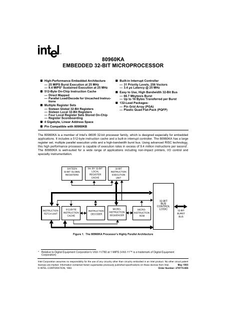
<strong>80960KA</strong>1.0 THE i960® PROCESSORThe <strong>80960KA</strong> is a member of the <strong>32</strong>-bit architecturefrom Intel known as the i960 processor family. Thesewere especially designed to serve the needs ofembedded applications. The embedded marketincludes applications as diverse as industrialautomation, avionics, image processing, graphics andnetworking. These types of applications require highintegration, low power consumption, quick interruptresponse times and high performance. Since time tomarket is critical, embedded microprocessors need tobe easy to use in both hardware and softwaredesigns.All members of the i960 processor family share acommon core architecture which utilizes RISCtechnology so that, except for special functions, thefamily members are object-code compatible. Eachnew processor in the family adds its own special setof functions to the core to satisfy the needs of aspecific application or range of applications in theembedded market.Software written for the <strong>80960KA</strong> will run withoutmodification on any other member of the 80960Family. It is also pin-compatible with the 80960KBwhich includes an integrated floating-point unit andthe 80960MC which is a military-grade version thatsupports multitasking, memory management, multiprocessingand fault tolerance.0000 0000HFFFF FFFFHADDRESS SPACEARCHITECTURALLYDEFINEDDATA STRUCTURESFETCH LOAD STOREINSTRUCTION CACHEINSTRUCTIONSTREAMINSTRUCTIONEXECUTIONPROCESSOR STATEREGISTERSSIXTEEN <strong>32</strong>-<strong>BIT</strong> GLOBAL REGISTERSREGISTER CACHEg0g15INSTRUCTIONPOINTERARITHMETICCONTROLSPROCESSCONTROLSTRACECONTROLSSIXTEEN <strong>32</strong>-<strong>BIT</strong> LOCAL REGISTERSFOUR 80-<strong>BIT</strong> FLOATING POINT REGISTERSCONTROL REGISTERSr0r15Figure 2. <strong>80960KA</strong> Programming Environment1
<strong>80960KA</strong>Table 1. <strong>80960KA</strong> Instruction SetData Movement Arithmetic Logical Bit and Bit FieldLoadStoreMoveLoad AddressAddSubtractMultiplyDivideRemainderModuloShiftAndNot AndAnd NotOrExclusive OrNot OrOr NotExclusive NorNotNandRotateSet BitClear BitNot BitCheck BitAlter BitScan For BitScan Over BitExtractModifyComparison Branch Call/Return FaultCompareConditional CompareCompare and IncrementCompare and DecrementUnconditional BranchConditional BranchCompare and BranchCallCall ExtendedCall SystemReturnBranch and LinkConditional FaultSynchronize FaultsDebug Miscellaneous DecimalModify Trace ControlsMarkForce MarkAtomic AddAtomic ModifyFlush Local RegistersModify Arithmetic ControlsScan Byte for EqualTest Condition CodeModify Process ControlsDecimal MoveDecimal Add with CarryDecimal Subtract withCarrySynchronousSynchronous LoadSynchronous Move3
<strong>80960KA</strong>ControlOpcodeDisplacementCompare andBranchOpcode Reg/Lit Reg M DisplacementRegister toRegisterOpcode Reg Reg/Lit Modes Ext’d Op Reg/LitMemory Access—ShortOpcode Reg Base M X OffsetMemory Access—LongOpcode Reg Base Mode Scale xx OffsetDisplacementFigure 3. Instruction Formats1.1.1. Memory Space And Addressing ModesThe <strong>80960KA</strong> offers a linear programming environmentso that all programs running on the processorare contained in a single address space. Maximumaddress space size is 4 Gigabytes (2 <strong>32</strong> bytes).For ease of use the <strong>80960KA</strong> has a small number ofaddressing modes, but includes all those necessaryto ensure efficient execution of high-level languagessuch as C. Table 2 lists the modes.Table 2. Memory Addressing Modes• 12-Bit Offset• <strong>32</strong>-Bit Offset• Register-Indirect• Register + 12-Bit Offset• Register + <strong>32</strong>-Bit Offset• Register + (Index-Register x Scale-Factor)• Register x Scale Factor + <strong>32</strong>-Bit Displacement• Register + (Index-Register x Scale-Factor) +<strong>32</strong>-Bit Displacement• Scale-Factor is 1, 2, 4, 8 or 161.1.2. Data TypesThe <strong>80960KA</strong> recognizes the following data types:Numeric:• 8-, 16-, <strong>32</strong>- and 64-bit ordinals• 8-, 16-, <strong>32</strong>- and 64-bit integersNon-Numeric:• Bit• Bit Field• Triple Word (96 bits)• Quad-Word (128 bits)1.1.3. Large Register SetThe <strong>80960KA</strong> programming environment includes alarge number of registers. In fact, <strong>32</strong> registers areavailable at any time. The availability of this manyregisters greatly reduces the number of memoryaccesses required to perform algorithms, which leadsto greater instruction processing speed.There are two types of general-purpose registers:local and global. The global registers consist ofsixteen <strong>32</strong>-bit registers (G0 though G15). Theseregisters perform the same function as the general-4
<strong>80960KA</strong>purpose registers provided in other popular microprocessors.The term global refers to the fact that theseregisters retain their contents across procedure calls.The local registers, on the other hand, are procedurespecific. For each procedure call, the <strong>80960KA</strong>allocates 16 local registers (R0 through R15). Eachlocal register is <strong>32</strong> bits wide.1.1.4. Multiple Register SetsTo further increase the efficiency of the register set,multiple sets of local registers are stored on-chip (SeeFigure 4). This cache holds up to four local registerframes, which means that up to three procedure callscan be made without having to access the procedurestack resident in memory.Although programs may have procedure calls nestedmany calls deep, a program typically oscillates backand forth between only two to three levels. As aresult, with four stack frames in the cache, the probabilityof having a free frame available on the cachewhen a call is made is very high. In fact, runs of representativeC-language programs show that 80% of thecalls are handled without needing to access memory.If four or more procedures are active and a newprocedure is called, the <strong>80960KA</strong> moves the oldestlocal register set in the stack-frame cache to aprocedure stack in memory to make room for a newset of registers. Global register G15 is the framepointer (FP) to the procedure stack.Global registers are not exchanged on a procedurecall, but retain their contents, making them availableto all procedures for fast parameter passing.1.1.5. Instruction CacheTo further reduce memory accesses, the <strong>80960KA</strong>includes a 512-byte on-chip instruction cache. Theinstruction cache is based on the concept of localityof reference; most programs are not usually executedin a steady stream but consist of many branches,loops and procedure calls that lead to jumping backand forth in the same small section of code. Thus, bymaintaining a block of instructions in cache, thenumber of memory references required to readinstructions into the processor is greatly reduced.To load the instruction cache, instructions are fetchedin 16-byte blocks; up to four instructions can befetched at one time. An efficient prefetch algorithmincreases the probability that an instruction willalready be in the cache when it is needed.Code for small loops often fits entirely within thecache, leading to a great increase in processingspeed since further memory references might not benecessary until the program exits the loop. Similarly,when calling short procedures, the code for thecalling procedure is likely to remain in the cache so itwill be there on the procedure’s return.1.1.6. Register ScoreboardingThe instruction decoder is optimized in several ways.One optimization method is the ability to overlapinstructions by using register scoreboarding.Register scoreboarding occurs when a LOAD movesa variable from memory into a register. When theinstruction initiates, a scoreboard bit on the targetregister is set. Once the register is loaded, the bit isreset. In between, any reference to the registercontents is accompanied by a test of the scoreboardbit to ensure that the load has completed beforeprocessing continues. Since the processor does notneed to wait for the LOAD to complete, it can executeadditional instructions placed between the LOAD andthe instruction that uses the register contents, asshown in the following example:ld data_2, r4ld data_2, r5Unrelated instructionUnrelated instructionadd R4, R5, R6In essence, the two unrelated instructions betweenLOAD and ADD are executed “for free” (i.e., take noapparent time to execute) because they are executedwhile the register is being loaded. Up to three loadinstructions can be pending at one time with threecorresponding scoreboard bits set. By exploiting thisfeature, system programmers and compiler writershave a useful tool for optimizing execution speed.5
<strong>80960KA</strong>ONE OF FOURLOCALREGISTER SETSREGISTERCACHELOCAL REGISTER SETR 031 0R 15Figure 4. Multiple Register Sets Are Stored On-Chip1.1.7. High Bandwidth Local BusThe <strong>80960KA</strong> CPU resides on a high-bandwidthaddress/data bus known as the local bus (L-Bus). TheL-Bus provides a direct communication path betweenthe processor and the memory and I/O subsysteminterfaces. The processor uses the L-Bus to fetchinstructions, manipulate memory and respond tointerrupts. L-Bus features include:• <strong>32</strong>-bit multiplexed address/data path• Four-word burst capability which allows transfersfrom 1 to 16 bytes at a time• High bandwidth reads and writes with66.7 MBytes/s burst (at 25 MHz)Table 3 defines L-bus signal names and functions;Table 4 defines other component-support signalssuch as interrupt lines.1.1.8. Interrupt HandlingThe <strong>80960KA</strong> can be interrupted in two ways: by theactivation of one of four interrupt pins or by sending amessage on the processor’s data bus.The <strong>80960KA</strong> is unusual in that it automaticallyhandles interrupts on a priority basis and can keeptrack of pending interrupts through its on-chipinterrupt controller. Two of the interrupt pins can beconfigured to provide 8259A-style handshaking forexpansion beyond four interrupt lines.1.1.9. Debug FeaturesThe <strong>80960KA</strong> has built-in debug capabilities. Thereare two types of breakpoints and six trace modes.Debug features are controlled by two internal <strong>32</strong>-bitregisters: the Process-Controls Word and the Trace-Controls Word. By setting bits in these control words,a software debug monitor can closely control how theprocessor responds during program execution.The <strong>80960KA</strong> provides two hardware breakpointregisters on-chip which, by using a special command,can be set to any value. When the instruction pointermatches either breakpoint register value, thebreakpoint handling routine is automatically called.The <strong>80960KA</strong> also provides software breakpointsthrough the use of two instructions: MARK andFMARK. These can be placed at any point in aprogram and cause the processor to halt execution atthat point and call the breakpoint handling routine.The breakpoint mechanism is easy to use andprovides a powerful debugging tool.Tracing is available for instructions (single stepexecution), calls and returns and branching. Eachtrace type may be enabled separately by a special6
<strong>80960KA</strong>debug instruction. In each case, the <strong>80960KA</strong>executes the instruction first and then calls a tracehandling routine (usually part of a software debugmonitor). Further program execution is halted until theroutine completes, at which time execution resumesat the next instruction. The <strong>80960KA</strong>’s tracingmechanisms, implemented completely in hardware,greatly simplify the task of software test and debug.1.1.10. Fault DetectionThe <strong>80960KA</strong> has an automatic mechanism to handlefaults. Fault types include trace and arithmetic faults.When the processor detects a fault, it automaticallycalls the appropriate fault handling routine and savesthe current instruction pointer and necessary stateinformation to make efficient recovery possible. Likeinterrupt handling routines, fault handling routines areusually written to meet the needs of specific applicationsand are often included as part of the operatingsystem or kernel.For each of the fault types, there are numeroussubtypes that provide specific information about afault. The fault handler can use this specific informationto respond correctly to the fault.1.1.11. Built-in TestabilityUpon reset, the <strong>80960KA</strong> automatically conducts anexhaustive internal test of its major blocks of logic.Then, before executing its first instruction, it does azero check sum on the first eight words in memory toensure that the memory image was programmedcorrectly. If a problem is discovered at any pointduring the self-test, the <strong>80960KA</strong> asserts its FAILUREpin and will not begin program execution. Self testtakes approximately 47,000 cycles to complete.System manufacturers can use the <strong>80960KA</strong>’s selftestfeature during incoming parts inspection. Nospecial diagnostic programs need to be written. Thetest is both thorough and fast. The self-test capabilityhelps ensure that defective parts are discoveredbefore systems are shipped and, once in the field, theself-test makes it easier to distinguish betweenproblems caused by processor failure and problemsresulting from other causes.1.1.12. CHMOSThe <strong>80960KA</strong> is fabricated using Intel’s CHMOS IV(Complementary High Speed Metal Oxide Semiconductor)process. The <strong>80960KA</strong> is currently availablein 16, 20 and 25 MHz versions.7
<strong>80960KA</strong>Table 3. <strong>80960KA</strong> Pin Description: L-Bus Signals (Sheet 1 of 2)NAME TYPE DESCRIPTIONCLK2 I SYSTEM CLOCK provides the fundamental timing for <strong>80960KA</strong> systems. It is dividedby two inside the <strong>80960KA</strong> to generate the internal processor clock.LAD31:0ALEADSW/RDT/RI/OT.S.OT.S.OO.D.OO.D.OO.D.LOCAL ADDRESS / DATA BUS carries <strong>32</strong>-bit physical addresses and data to andfrom memory. During an address (T a ) cycle, bits 2-31 contain a physical wordaddress (bits 0-1 indicate SIZE; see below). During a data (T d ) cycle, bits 0-31contain read or write data. These pins float to a high impedance state when notactive.Bits 0-1 comprise SIZE during a T a cycle. SIZE specifies burst transfer size in words.LAD1 LAD00 0 1 Word0 1 2 Words1 0 3 Words1 1 4 WordsADDRESS LATCH ENABLE indicates the transfer of a physical address. ALE isasserted during a T a cycle and deasserted before the beginning of the T d state. It isactive LOW and floats to a high impedance state during a hold cycle (T h ).ADDRESS/DATA STATUS indicates an address state. ADS is asserted every T astate and deasserted during the following T d state. For a burst transaction, ADS isasserted again every T d state where READY was asserted in the previous cycle.WRITE/READ specifies, during a T a cycle, whether the operation is a write or read. Itis latched on-chip and remains valid during T d cycles.DATA TRANSMIT / RECEIVE indicates the direction of data transfer to and from theL-Bus. It is low during T a and T d cycles for a read or interrupt acknowledgment; it ishigh during T a and T d cycles for a write. DT/R never changes state when DEN isasserted.READY I READY indicates that data on LAD lines can be sampled or removed. If READY is notasserted during a T d cycle, the T d cycle is extended to the next cycle by inserting await state (T w ) and ADS is not asserted in the next cycle.LOCKI/OO.D.BUS LOCK prevents bus masters from gaining control of the L-Bus duringRead/Modify/Write (RMW) cycles. The processor or any bus agent may assertLOCK.At the start of a RMW operation, the processor examines the LOCK pin. If the pin isalready asserted, the processor waits until it is not asserted. If the pin is not asserted,the processor asserts LOCK during the T a cycle of the read transaction. Theprocessor deasserts LOCK in the T a cycle of the write transaction. During the timeLOCK is asserted, a bus agent can perform a normal read or write but not a RMWoperation.The processor also asserts LOCK during interrupt-acknowledge transactions.Do not leave LOCK unconnected. It must be pulled high for the processor to functionproperly.I/O = Input/Output, O = Output, I = Input, O.D. = Open Drain, T.S. = Three-state8
<strong>80960KA</strong>BE3:0OO.D.BYTE ENABLE LINES specify the data bytes (up to four) on the bus which are usedin the current bus cycle. BE3 corresponds to LAD31:24; BE0 corresponds to LAD7:0.The byte enables are provided in advance of data:• Byte enables asserted during T a specify the bytes of the first data word.• Byte enables asserted during T d specify the bytes of the next data word, if any (theword to be transmitted following the next assertion of READY).Byte enables that occur during T d cycles that precede the last assertion of READYare undefined. Byte enables are latched on-chip and remain constant from one T dcycle to the next when READY is not asserted.For reads, byte enables specify the byte(s) that the processor will actually use. L-Busagents are required to assert only adjacent byte enables (e.g., asserting just BE0 andBE2 is not permitted) and are required to assert at least one byte enable. Addressbits A 0 and A 1 can be decoded externally from the byte enables.HOLD I HOLD: A request from an external bus master to acquire the bus. When theprocessor receives HOLD and grants bus control to another master, it floats its threestatebus lines and open-drain control lines, asserts HLDA and enters the T h state.When HOLD deasserts, the processor deasserts HLDA and enters the T i or T a state.HLDACACHEOT.S.OT.S.Table 3. <strong>80960KA</strong> Pin Description: L-Bus Signals (Sheet 2 of 2)NAME TYPE DESCRIPTIONHOLD ACKNOWLEDGE: Notifies an external bus master that the processor hasrelinquished control of the bus.CACHE indicates when an access is cacheable during a T a cycle. It is not assertedduring any synchronous access, such as a synchronous load or move instructionused for sending an IAC message. The CACHE signal floats to a high impedancestate when the processor is idle.I/O = Input/Output, O = Output, I = Input, O.D. = Open Drain, T.S. = Three-stateTable 4. <strong>80960KA</strong> Pin Description: Support Signals (Sheet 1 of 2)NAME TYPE DESCRIPTIONBADAC I BAD ACCESS, if asserted in the cycle following the one in which the last READY of atransaction is asserted, indicates an unrecoverable error occurred on the current bustransaction or a synchronous load/store instruction has not been acknowledged.During system reset the BADAC signal is interpreted differently. If the signal is high, itindicates that this processor will perform system initialization. If it is low, anotherprocessor in the system will perform system initialization instead.RESET I RESET clears the processor’s internal logic and causes it to reinitialize.During RESET assertion, the input pins are ignored (except for BADAC andIAC/INT 0 ), the three-state output pins are placed in a high impedance state and otheroutput pins are placed in their non-asserted states.RESET must be asserted for at least 41 CLK2 cycles for a predictable RESET. TheHIGH to LOW transition of RESET should occur after the rising edge of both CLK2and the external bus clock and before the next rising edge of CLK2.I/O = Input/Output, O = Output, I = Input, O.D. = Open Drain, T.S. = Three-state9
<strong>80960KA</strong>FAILUREOO.D.INITIALIZATION FAILURE indicates that the processor did not initialize correctly.After RESET deasserts and before the first bus transaction begins, FAILURE assertswhile the processor performs a self-test. If the self-test completes successfully, thenFAILURE deasserts. The processor then performs a zero checksum on the first eightwords of memory. If it fails, FAILURE asserts for a second time and remainsasserted. If it passes, system initialization continues and FAILURE remainsdeasserted.IAC/INT 0 I INTERAGENT COMMUNICATION REQUEST/INTERRUPT 0 indicates an IACmessage or an interrupt is pending. The bus interrupt control register determines howthe signal is interpreted. To signal an interrupt or IAC request in a synchronoussystem, this pin — as well as the other interrupt pins — must be enabled by beingdeasserted for at least one bus cycle and then asserted for at least one additionalbus cycle. In an asynchronous system the pin must remain deasserted for at leasttwo bus cycles and then asserted for at least two more bus cycles.During system reset, this signal must be in the logic high condition to enable normalprocessor operation. The logic low condition is reserved.INT 1 I INTERRUPT 1, like INT 0 , provides direct interrupt signaling.INT 2 /INTR I INTERRUPT2/INTERRUPT REQUEST: The interrupt control register determineshow this pin is interpreted. If INT 2 , it has the same interpretation as the INT 0 and INT 1pins. If INTR, it is used to receive an interrupt request from an external interruptcontroller.INT 3 /INTAI/OO.D.Table 4. <strong>80960KA</strong> Pin Description: Support Signals (Sheet 2 of 2)NAME TYPE DESCRIPTIONINTERRUPT3/INTERRUPT ACKNOWLEDGE: The bus interrupt control registerdetermines how this pin is interpreted. If INT 3 , it has the same interpretation as theINT 0 , INT1 and INT2 pins. If INTA, it is used as an output to control interruptacknowledgetransactions. The INTA output is latched on-chip and remains validduring T d cycles; as an output, it is open-drain.N.C. N/A NOT CONNECTED indicates pins should not be connected. Never connect any pinmarked N.C. as these pins may be reserved for factory use.I/O = Input/Output, O = Output, I = Input, O.D. = Open Drain, T.S. = Three-state2.0 ELECTRICAL SPECIFICATIONS2.1. Power and GroundingThe <strong>80960KA</strong> is implemented in CHMOS IVtechnology and therefore has modest power requirements.Its high clock frequency and numerous outputbuffers (address/data, control, error and arbitrationsignals) can cause power surges as multiple outputbuffers simultaneously drive new signal levels. Forclean on-chip power distribution, V CC and V SS pinsseparately feed the device’s functional units. Powerand ground connections must be made to all<strong>80960KA</strong> power and ground pins. On the circuitboard, all V cc pins must be strapped closely together,preferably on a power plane; all V ss pins should bestrapped together, preferably on a ground plane.2.2. Power DecouplingRecommendationsPlace a liberal amount of decoupling capacitancenear the <strong>80960KA</strong>. When driving the L-bus theprocessor can cause transient power surges, particularlywhen connected to a large capacitive load.Low inductance capacitors and interconnects arerecommended for best high frequency electricalperformance. Inductance is reduced by shorteningboard traces between the processor and decouplingcapacitors as much as possible.10
<strong>80960KA</strong>2.3. Connection RecommendationsFor reliable operation, always connect unused inputsto an appropriate signal level. In particular, if one ormore interrupt lines are not used, they should bepulled up. No inputs should ever be left floating.OPEN-DRAIN OUTPUTV CC180 ΩAll open-drain outputs require a pullup device. Whilein most cases a simple pullup resistor is adequate, anetwork of pullup and pulldown resistors biased to avalid V IH (>3.0 V) and terminated in the characteristicimpedance of the circuit board is recommended tolimit noise and AC power consumption. Figure 5 andFigure 6 show recommended values for the resistornetwork for low and high current drive, assuming acharacteristic impedance of 100 Ω. Terminatingoutput signals in this fashion limits signal swing andreduces AC power consumption.NOTE:Do not connect external logic to pins marked N.C.OPEN-DRAIN OUTPUTLow Drive Network:V OH = 3.0 VI OL = 20.7 mAV CC220 Ω330 ΩHigh Drive Network:V OH = 3.4 VI OL = 25.3 mAFigure 6. Connection Recommendationsfor High Current Drive Network2.4. Characteristic Curves390 ΩFigure 7 shows typical supply current requirementsover the operating temperature range of theprocessor at supply voltage (V CC ) of 5 V. Figure 8 andFigure 9 show the typical power supply current (I CC )that the <strong>80960KA</strong> requires at various operatingfrequencies when measured at three input voltage(V CC ) levels and two temperatures.For a given output current (I OL ) the curve in Figure 10shows the worst case output low voltage (V OL ). Figure11 shows the typical capacitive derating curve for the<strong>80960KA</strong> measured from 1.5V on the system clock(CLK) to 1.5V on the falling edge and 1.5V on therising edge of the L-Bus address/data (LAD) signals.Figure 5. Connection Recommendationsfor Low Current Drive Network11
<strong>80960KA</strong>V CC = 5.0 V38025 MHz20 MHz16 MHzPOWER SUPPLY CURRENT (mA)360340<strong>32</strong>0300280260240220200-60 -40 -20 0 20 40 60 80 100 120 140CASE TEMPERATURE (°C)Figure 7. Typical Supply Current vs. Case TemperatureTEMP = +22°C@5.5V@5.0V@4.5VTYPICAL SUPPLY CURRENT (mA)400380360340<strong>32</strong>030028026024022020018016 20 25OPERATING FREQUENCY (MHz)Figure 8. Typical Current vs. Frequency (Room Temp)12
<strong>80960KA</strong>TEMP = +22°C@5.5V@5.0V@4.5VTYPICAL SUPPLY CURRENT (mA)380360340<strong>32</strong>030028026024022020018016016 20 25OPERATING FREQUENCY (MHz)Figure 9. Typical Current vs. Frequency (Hot Temp)(TEMP = +85°C, V CC = 4.5V)OUTPUT LOW VOLTAGE (V)0.80.60.40.20.00 10 20 30 40 50OUTPUT LOW CURRENT(mA)Figure 10. Worst-Case Voltage vs. Output Currenton Open-Drain Pins(TEMP = +85°C, V CC = 4.5V)30FALLING25THREE-STATE OUTPUTVALID DELAY(ns)2015105RISING00 20 40 60 80 100CAPACITIVE LOAD(pF)Figure 11. Capacitive Derating Curve13
<strong>80960KA</strong>2.5. Test Load CircuitFigure 12 illustrates the load circuit used to test the<strong>80960KA</strong>’s three-state pins; Figure 13 shows the loadcircuit used to test the open drain outputs. The opendrain test uses an active load circuit in the form of amatched diode bridge. Since the open-drain outputssink current, only the I OL legs of the bridge arenecessary and the I OH legs are not used. When the<strong>80960KA</strong> driver under test is turned off, the output pinis pulled up to V REF (i.e., V OH ). Diode D 1 is turned offand the I OL current source flows through diode D 2 .THREE-STATE OUTPUTC LC L = 50 pF for all signalsFigure 12. Test Load Circuit for Three-State Output PinsWhen the <strong>80960KA</strong> open-drain driver under test ison, diode D 1 is also on and the voltage on the pinbeing tested drops to V OL . Diode D 2 turns off and I OLflows through diode D 1 .OPEN-DRAIN OUTPUTD 1C LC L = 50 pF for all signalsI OLD 2I OL Tested at 25 mAV REF = V CCD1 and D 2 are matchedFigure 13. Test Load Circuit for Open-Drain Output Pins14
<strong>80960KA</strong>2.6. Absolute Maximum Ratings NOTICE: This is a production data sheet. The specificationsare subject to change without notice.Operating Temperature (PGA).............. 0°C to +85°C Case(PQFP) ......... 0°C to +100°C CaseStorage Temperature ................................. –65°C to +150°CVoltage on Any Pin................................. –0.5V to V CC +0.5VPower Dissipation .......................................... 2.5W (25 MHz)2.7. DC CharacteristicsPGA: <strong>80960KA</strong> (16 MHz) T CASE = 0°C to +85°C, V CC = 5V ± 10%<strong>80960KA</strong> (20 and 25 MHz) T CASE = 0°C to +85°C, V CC = 5V ± 5%PQFP: <strong>80960KA</strong> (16 MHz) T CASE = 0°C to +100°C, V CC = 5V ± 10%<strong>80960KA</strong> (20 and 25 MHz) T CASE = 0°C to +100°C, V CC = 5V ± 5%*WARNING: Stressing the device beyond the “Absolute MaximumRatings” may cause permanent damage. These arestress ratings only. Operation beyond the “Operating Conditions”is not recommended and extended exposure beyond the“Operating Conditions” may affect device reliability.Table 5. DC CharacteristicsSymbol Parameter Min Max Units NotesV IL Input Low Voltage –0.3 +0.8 VV IH Input High Voltage 2.0 V CC + 0.3 VV CL CLK2 Input Low Voltage –0.3 +0.8 VV CH CLK2 Input High Voltage 0.55 V CC V CC + 0.3 VV OL Output Low Voltage 0.45 V (1,2)V OH Output High Voltage 2.4 V (3,4)I CCPower Supply Current:16 MHz20 MHz25 MHzI LI Input Leakage Current ±15 µA 0 ≤ V IN ≤ V CCI LO Output Leakage Current ±15 µA 0.45 ≤ V O ≤ V CCC IN Input Capacitance 10 pF f C = 1 MHz (6)C O Output Capacitance 12 pF f C = 1 MHz (6)C CLK Clock Capacitance 10 pF f C = 1 MHz (6)NOTES:1. For three-state outputs, this parameter is measured at:Address/Data............................................................................................................................................................................................. 4.0 mAControls ...................................................................................................................................................................................................... 5.0 mA2. For open-drain outputs ................................................................................................................................................................................ 25 mA3. This parameter is measured at:Address/Data ........................................................................................................................................................................................... -1.0 mAControls .................................................................................................................................................................................................... -0.9 mAALE .......................................................................................................................................................................................................... -5.0 mA4. Not measured on open-drain outputs.5. Measured at worst case frequency, V CC and temperature, with device operating and outputs loaded to the test conditions in Figures 12 and 13.Figure 7, Figure 8 and Figure 9 indicate typical values.6. Input, output and clock capacitance are not tested.15315360420mAmAmA(5)(5)(5)
<strong>80960KA</strong>2.8. AC SpecificationsThis section describes the AC specifications for the<strong>80960KA</strong> pins. All input and output timings arespecified relative to the 1.5 V level of the rising edgeof CLK2. For output timings the specifications refer tothe time it takes the signal to reach 1.5 V.For input timings the specifications refer to the time atwhich the signal reaches (for input setup) or leaves(for hold time) the TTL levels of LOW (0.8 V) or HIGH(2.0 V). All AC testing should be done with inputvoltages of 0.4 V and 2.4 V, except for the clock(CLK2), which should be tested with input voltages of0.45 V and 0.55 V CC .EDGEA B C D A B CCLK21.5V 1.5V 1.5V 1.5V0.8VT 61.5V 1.5VOUTPUTS:LAD 31:0ADSW/R, DENBE3:0HLDACACHELOCK, INTAT 91.5V VALID OUTPUT 1.5VT 8T 8T 13 T 14ALET 7T 6T 9DT/R1.5V VALID OUTPUT 1.5VINPUTS:LAD31:0BADACIAC/INT0, INT1INT2/INTR, INT3HOLDLOCKREADYT 10 T 112.0V 2.0V0.8V 0.8VT 12 T 112.0V 2.0V0.8V 0.8VVALID INPUTFigure 14. Drive Levels and Timing Relationships for <strong>80960KA</strong> Signals16
<strong>80960KA</strong>2.8.1. AC Specification Tables1. Clock rise and fall times are not tested.Table 6. <strong>80960KA</strong> AC Characteristics (16 MHz)Symbol Parameter Min Max Units NotesInput ClockT 1 Processor Clock Period (CLK2) 31.25 125 ns V IN = 1.5VT 2 Processor Clock Low Time (CLK2) 8 ns V IL = 10% Point = 1.2VT 3Processor Clock High Time(CLK2)8 ns V IH = 90% Point = 0.1V + 0.5 V CCT 4 Processor Clock Fall Time (CLK2) 10 ns V IN = 90% Point to 10% Point (1)T 5 Processor Clock Rise Time (CLK2) 10 ns V IN = 10% Point to 90% Point (1)Synchronous OutputsT 6 Output Valid Delay 2 25 nsT 6H HLDA Output Valid Delay 4 28 nsT 7 ALE Width 15 nsT 8 ALE Output Valid Delay 2 18 nsT 9 Output Float Delay 2 20 ns (2)T 9H HLDA Output Float Delay 4 20 ns (2)Synchronous InputsT 10 Input Setup 1 3 ns (3)T 11 Input Hold 5 ns (3)T 11H HOLD Input Hold 4 ns (3)T 12 Input Setup 2 8 ns (3)T 13 Setup to ALE Inactive 10 nsT 14 Hold after ALE Inactive 8 nsT 15 Reset Hold 3 ns (3)T 16 Reset Setup 5 ns (3)T 17 Reset Width 1281 ns 41 CLK2 Periods MinimumNOTES:2. A float condition occurs when the maximum output current becomes less than I LO . Float delay is not tested; however, it should not be longer thanthe valid delay.3. LAD31:0, BADAC, HOLD, LOCK and READY are synchronous inputs. IAC/INT 0 , INT 1 , INT 2 /INT R and INT 3 may be synchronous or asynchronous.17
<strong>80960KA</strong>1. Clock rise and fall times are not tested.Table 7. <strong>80960KA</strong> AC Characteristics (20 MHz)Symbol Parameter Min Max Units NotesInput ClockT 1 Processor Clock Period (CLK2) 25 125 ns V IN = 1.5VT 2 Processor Clock Low Time (CLK2) 6 ns V IL = 10% Point = 1.2VT 3Processor Clock High Time(CLK2)6 ns V IH = 90% Point = 0.1V + 0.5 V CCT 4 Processor Clock Fall Time (CLK2) 10 ns V IN = 90% Point to 10% Point (1)T 5 Processor Clock Rise Time (CLK2) 10 ns V IN = 10% Point to 90% Point (1)Synchronous OutputsT 6 Output Valid Delay 2 20 nsT 6H HLDA Output Valid Delay 4 23 nsT 7 ALE Width 12 nsT 8 ALE Output Valid Delay 2 18 nsT 9 Output Float Delay 2 20 ns (2)T 9H HLDA Output Float Delay 4 20 ns (2)Synchronous InputsT 10 Input Setup 1 3 ns (3)T 11 Input Hold 5 ns (3)T 11H HOLD Input Hold 4 ns (3)T 12 Input Setup 2 7 ns (3)T 13 Setup to ALE Inactive 10 nsT 14 Hold after ALE Inactive 8 nsT 15 Reset Hold 3 nsT 16 Reset Setup 5 nsT 17 Reset Width 1025 ns 41 CLK2 Periods MinimumNOTES:2. A float condition occurs when the maximum output current becomes less than I LO . Float delay is not tested; however, it should not be longer thanthe valid delay.3. LAD31:0, BADAC, HOLD, LOCK and READY are synchronous inputs. IAC/INT 0 , INT 1 , INT 2 /INT R and INT 3 may be synchronous or asynchronous.18
<strong>80960KA</strong>1. Clock rise and fall times are not tested.Table 8. <strong>80960KA</strong> AC Characteristics (25 MHz)Symbol Parameter Min Max Units NotesInput ClockT 1 Processor Clock Period (CLK2) 20 125 ns V IN = 1.5VT 2 Processor Clock Low Time (CLK2) 5 ns V IL = 10% Point = 1.2VT 3Processor Clock High Time(CLK2)5 ns V IH = 90% Point = 0.1V + 0.5 V CCT 4 Processor Clock Fall Time (CLK2) 10 ns V IN = 90% Point to 10% Point (1)T 5 Processor Clock Rise Time (CLK2) 10 ns V IN = 10% Point to 90% Point (1)Synchronous OutputsT 6 Output Valid Delay 2 18 nsT 6H HLDA Output Valid Delay 4 23 nsT 7 ALE Width 12 nsT 8 ALE Output Valid Delay 2 18 nsT 9 Output Float Delay 2 18 ns (2)T 9H HLDA Output Float Delay 4 20 ns (2)Synchronous InputsT 10 Input Setup 1 3 ns (3)T 11 Input Hold 5 ns (3)T 11H HOLD Input Hold 4 nsT 12 Input Setup 2 7 nsT 13 Setup to ALE Inactive 8 nsT 14 Hold after ALE Inactive 8 nsT 15 Reset Hold 3 nsT 16 Reset Setup 5 nsT 17 Reset Width 820 ns 41 CLK2 Periods MinimumNOTES:2. A float condition occurs when the maximum output current becomes less than I LO . Float delay is not tested; however, it should not be longer thanthe valid delay.3. LAD31:0, BADAC, HOLD, LOCK and READY are synchronous inputs. IAC/INT 0 , INT 1 , INT 2 /INT R and INT 3 may be synchronous or asynchronous.19
<strong>80960KA</strong>T 3T 1HIGH LEVEL (MIN) 0.55V CC90%1.5 VLOW LEVEL (MAX) 0.8V10%T 5 T 4T 2Figure 15. Processor Clock Pulse (CLK2)CLK2CLKRESETOUTPUTS.........T 17...T 15 T 16FIRSTA B C D AINIT PARAMETERS (BADAC,INT 0 /IAC) MUST BE SET UP 8 CLOCKSPRIOR TO THIS CLK2 EDGEINIT PARAMETERS MUST BE HELDBEYOND THIS CLK2 EDGET 15 = RESET HOLDT 16 = RESET SETUPT 17 = RESET WIDTHFigure 16. RESET Signal Timing20
<strong>80960KA</strong>3.0 MECHANICAL DATA3.1. PackagingThe <strong>80960KA</strong> is available in two package types:• 1<strong>32</strong>-lead ceramic pin-grid array (PGA). Pins arearranged 0.100 inch (2.54 mm) center-to-center, ina 14 by 14 matrix, three rows around (see Figure17).• 1<strong>32</strong>-lead plastic quad flat pack (PQFP). Thispackage uses fine-pitch gull wing leads arranged ina single row along the package perimeter with0.025 inch (0.64 mm) spacing (see Figure 20).3.1.1. Pin AssignmentThe PGA and PQFP have different pin assignments.Figure 18 shows the view from the PGA bottom (pinsfacing up) and Figure 19 shows a view from the PGAtop (pins facing down). Figure 20 shows the PQFPpackage; Figure 21 shows the PQFP pinout withsignal names. Notice that the pins are numbered inorder from 1 to 1<strong>32</strong> around the package perimeter.Table 9 and Table 10 list the function of each PGApin; Table 11 and Table 12 list the function of eachPQFP pin.Dimensions for both package types are given in theIntel Packaging handbook (Order #240800).1234567891011121314A B C D E F G H J K L M N PFigure 17. 1<strong>32</strong>-Lead Pin-Grid Array (PGA) Package21
<strong>80960KA</strong>1234567891011121314PNMLKJHGFEDCBAV CCV SSN.C.DENBE 3DT/RW/RN.C.N.C.N.C.N.C.FAILBE 2READYLAD 30N.C.N.C.V SSV CCV SSV SSBE 0 LOCKBE 1LAD 29 LAD 31 CACHELAD 28 LAD 26 LAD 27ALEADS HLDAN.C.N.C.V SSN.C.N.C.V CCN.C.N.C.N.C.N.C.N.C.N.C.HOLD LAD 25 BADAC V CC V SS LAD 20 LAD 13 LAD 8 LAD 3 V CC V SS INT 3 INT 1 INT 0LAD 23 LAD 24 LAD 22 LAD 21 LAD 18 LAD 15 LAD 12 LAD 10 LAD 6 LAD 2 CLK2 LAD 0 RESET V SSV CC V SS LAD 19LAD 17 LAD 16 LAD 14 LAD 11 LAD 9 LAD 7 LAD 5 LAD 4 LAD 1 INT 2 V CCN.C.N.C.N.C.N.C.N.C.N.C.N.C.N.C.V SSN.C.N.C.V CCN.C.N.C.N.C.V SSV CCN.C.N.C.N.C.N.C.N.C.V CCV SSN.C.V CCN.C.N.C.N.C.N.C.N.C.N.C.V SSN.C.V CCN.C.N.C.N.C.N.C.N.C.N.C.N.C.N.C.N.C.N.C.PNMLKJHGFEDCBA1234567891011121314Figure 18. <strong>80960KA</strong> PGA Pinout—View from Bottom (Pins Facing Up)22
<strong>80960KA</strong>14 13 12 11 10 9 8 7 6 5 4 3 2 1PPNMLKJHGFEDCBAV CC V SS N.C. N.C. N.C. N.C. N.C. N.C. N.C. N.C. N.C. N.C. N.C. V CCN.C. N.C. N.C. N.C. N.C. N.C. N.C. N.C. N.C. N.C. N.C. N.C. N.C. V SSN.C. N.C. N.C. V CC V SS N.C. N.C. N.C. N.C. V CC V SS V SS V CC N.C.N.C.N.C.N.C.N.C.V SSV CCN.C. N.C. N.C.N.C. N.C. N.C.N.C. N.C. N.C.N.C. N.C. N.C.A<strong>80960KA</strong>-25XXXXXXXXXXXXXXXXXXXXV CC N.C. DENV SS FAIL BE 3V SS BE 2 DT/RLOCK BE 0 W/RBE 1 READY LAD 30CACHE LAD 31 LAD 29N.C. V SS N.C.LAD 27 LAD 26 LAD 28N.C. N.C. V CC HLDA ADS ALEINT 0 INT 1 INT 3 V SS V CC LAD 3 LAD 8 LAD 13 LAD 20 V CC BADAC LAD 25 HOLDV SSV SS RESET LAD 0 CLK2 LAD 2 LAD 6 LAD 10 LAD 12 LAD 15 LAD 18 LAD 21 LAD 22 LAD 24 LAD 23V SS V CCNMLKJHGFEDCBAV CC INT 2LAD 1 LAD 4 LAD 5 LAD 7 LAD 9 LAD 11 LAD 14 LAD 16 LAD 17 LAD 1914 13 12 11 10 9 8 7 6 5 4 3 2 1Figure 19. <strong>80960KA</strong> PGA Pinout—View from Top (Pins Facing Down)Figure 20. <strong>80960KA</strong> 1<strong>32</strong>-Lead Plastic Quad Flat-Pack (PQFP) Package23
<strong>80960KA</strong>V SSNCNCNCNCNCRESETV CCCLK2V SSNCINT3/INTAINT2/INTRINT1IAC/INT0V SSV CCV CCNCV SSV SSNCNCNCNCV CCV SSNCV CCV CCNCV SSV SSLAD0LAD1LAD2V SSLAD3LAD4LAD5LAD6LAD7LAD8LAD9LAD10LAD11LAD12V SSLAD13LAD14LAD15LAD16LAD17LAD18LAD19LAD20LAD21LAD22V SSLAD23LAD24LAD25BADACHOLDNCADS1001011021031041051061071081091101111121131141151161171181191201211221231241251261271281291301311<strong>32</strong>99 98 97 96 95 94 93 92 91 90 89 88 87 86 85 84 83 82 81 80 79 78 77 76 75 74 73 72 71 70 69 68 67NG<strong>80960KA</strong>-25XXXXXXXXXXXXXXXXXXXX1 2 3 4 5 6 7 8 9 10 11 12 13 14 15 16 17 18 19 20 21 22 23 24 25 26 27 28 29 30 31 <strong>32</strong> 33666564636261605958575655545352515049484746454443424140393837363534NCNCNCNCNCNCNCNCNCV SSV CCV CCNCV SSV SSNCNCNCNCNCNCNCNCNCV SSV CCNCNCNCNCV CCV CCNCHLDAALELAD26LAD27LAD28LAD29LAD30LAD31V SSCACHEW/RREADYDT/RBE0BE1BE2BE3FAILUREV SSLOCKDENV SSV SSNCNCV SSV SSNCV CCV CCNCV SSV SSFigure 21. PQFP Pinout - View From Top24
<strong>80960KA</strong>3.2. PinoutTable 9. <strong>80960KA</strong> PGA Pinout — In Pin OrderPin Signal Pin Signal Pin Signal Pin SignalA1 V CC C6 LAD 20 H1 W/R M10 V SSA2 V SS C7 LAD 13 H2 BE 0 M11 V CCA3 LAD 19 C8 LAD 8 H3 LOCK M12 N.C.A4 LAD 17 C9 LAD 3 H12 N.C. M13 N.C.A5 LAD 16 C10 V CC H13 N.C. M14 N.C.A6 LAD 14 C11 V SS H14 N.C. N1 V SSA7 LAD 11 C12 INT 3 /INTA J1 DT/R N2 N.C.A8 LAD 9 C13 INT 1 J2 BE 2 N3 N.C.A9 LAD 7 C14 IAC/INT 0 J3 V SS N4 N.C.A10 LAD 5 D1 ALE J12 N.C. N5 N.C.A11 LAD 4 D2 ADS J13 N.C. N6 N.C.A12 LAD 1 D3 HLDA J14 N.C. N7 N.C.A13 INT 2 /INTR D12 V CC K1 BE 3 N8 N.C.A14 V CC D13 N.C. K2 FAILURE N9 N.C.B1 LAD 23 D14 N.C. K3 V SS N10 N.C.B2 LAD 24 E1 LAD 28 K12 V CC N11 N.C.B3 LAD 22 E2 LAD 26 K13 N.C. N12 N.C.B4 LAD 21 E3 LAD 27 K14 N.C. N13 N.C.B5 LAD 18 E12 N.C. L1 DEN N14 N.C.B6 LAD 15 E13 V SS L2 N.C. P1 V CCB7 LAD 12 E14 N.C. L3 V CC P2 N.C.B8 LAD 10 F1 LAD 29 L12 V SS P3 N.C.B9 LAD 6 F2 LAD 31 L13 N.C. P4 N.C.B10 LAD 2 F3 CACHE L14 N.C. P5 N.C.B11 CLK2 F12 N.C. M1 N.C. P6 N.C.B12 LAD 0 F13 N.C. M2 V CC P7 N.C.B13 RESET F14 N.C. M3 V SS P8 N.C.B14 V SS G1 LAD 30 M4 V SS P9 N.C.C1 HOLD G2 READY M5 V CC P10 N.C.C2 LAD 25 G3 BE 1 M6 N.C. P11 N.C.C3 BADAC G12 N.C. M7 N.C. P12 N.C.C4 V CC G13 N.C. M8 N.C. P13 V SSC5 V SS G14 N.C. M9 N.C. P14 V CCNOTE:Do not connect any external logic to any pins marked N.C.25
<strong>80960KA</strong>Table 10. <strong>80960KA</strong> PGA Pinout — In Signal OrderSignal Pin Signal Pin Signal Pin Signal PinADS D2 LAD 15 B6 N.C. J14 N.C. P9ALE D1 LAD 16 A5 N.C. K13 N.C. P10BADAC C3 LAD 17 A4 N.C. K14 N.C. P11BE 0 H2 LAD 18 B5 N.C. L13 N.C. P12BE 1 G3 LAD 19 A3 N.C. L14 N.C. L2BE 2 J2 LAD 20 C6 N.C. M1 READY G2BE 3 K1 LAD 21 B4 N.C. M6 RESET B13CACHE F3 LAD 22 B3 N.C. M7 V CC A1CLK2 B11 LAD 23 B1 N.C. M8 V CC A14DEN L1 LAD 24 B2 N.C. M9 V CC C4DT/R J1 LAD 25 C2 N.C. M12 V CC C10FAILURE K2 LAD 26 E2 N.C. M13 V CC D12HLDA D3 LAD 27 E3 N.C. M14 V CC K12HOLD C1 LAD 28 E1 N.C. N2 V CC L3IAC/INT 0 C14 LAD 29 F1 N.C. N3 V CC M2INT 1 C13 LAD 30 G1 N.C. N4 V CC M5INT 2 /INTR A13 LAD 31 F2 N.C. N5 V CC M11INT 3 /INTA C12 LOCK H3 N.C. N6 V CC P1LAD 0 B12 N.C. D13 N.C. N7 V CC P14LAD 1 A12 N.C. D14 N.C. N8 V SS A2LAD 2 B10 N.C. E12 N.C. N9 V SS B14LAD 3 C9 N.C. E14 N.C. N10 V SS C5LAD 4 A11 N.C. F12 N.C. N11 V SS C11LAD 5 A10 N.C. F13 N.C. N12 V SS E11LAD 6 B9 N.C. F14 N.C. N13 V SS J3LAD 7 A9 N.C. G12 N.C. N14 V SS K3LAD 8 C8 N.C. G13 N.C. P2 V SS L12LAD 9 A8 N.C. G14 N.C. P3 V SS M3LAD 10 B8 N.C. H12 N.C. P4 V SS M4LAD 11 A7 N.C. H13 N.C. P5 V SS M10LAD 12 B7 N.C. H14 N.C. P6 V SS N1LAD 13 C7 N.C. J12 N.C. P7 V SS P13LAD 14 A6 N.C. J13 N.C. P8 W/R H1NOTE:Do not connect any external logic to any pins marked N.C.26
<strong>80960KA</strong>Table 11. <strong>80960KA</strong> PQFP Pinout — In Pin OrderPin Signal Pin Signal Pin Signal Pin Signal1 HLDA 34 N.C. 67 V SS 100 LAD 02 ALE 35 V CC 68 V SS 101 LAD 13 LAD 26 36 V CC 69 N.C. 102 LAD 24 LAD 27 37 N.C. 70 V CC 103 V SS5 LAD 28 38 N.C. 71 V CC 104 LAD 36 LAD 29 39 N.C. 72 N.C. 105 LAD 47 LAD 30 40 N.C. 73 V SS 106 LAD 58 LAD 31 41 V CC 74 V CC 107 LAD 69 V SS 42 V SS 75 N.C. 108 LAD 710 CACHE 43 N.C. 76 N.C. 109 LAD 811 W/R 44 N.C. 77 N.C. 110 LAD 912 READY 45 N.C. 78 N.C. 111 LAD 1013 DT/R 46 N.C. 79 V SS 112 LAD 1114 BE 0 47 N.C. 80 V SS 113 LAD 1215 BE 1 48 N.C. 81 N.C. 114 V SS16 BE 2 49 N.C. 82 V CC 115 LAD 1317 BE 3 50 N.C. 83 V CC 116 LAD 1418 FAILURE 51 N.C. 84 V SS 117 LAD 1519 V SS 52 V SS 85 IAC/INT 0 118 LAD 1620 LOCK 53 V SS 86 INT 1 119 LAD 1721 DEN 54 N.C. 87 INT 2 /INTR 120 LAD 1822 V SS 55 V CC 88 INT 3 /INTA 121 LAD 1923 V SS 56 V CC 89 N.C. 122 LAD 2024 N.C. 57 V SS 90 V SS 123 LAD 2125 N.C. 58 N.C. 91 CLK2 124 LAD 2226 V SS 59 N.C. 92 V CC 125 V SS27 V SS 60 N.C. 93 RESET 126 LAD 2<strong>32</strong>8 N.C. 61 N.C. 94 N.C. 127 LAD 2429 V CC 62 N.C. 95 N.C. 128 LAD 2530 V CC 63 N.C. 96 N.C. 129 BADAC31 N.C. 64 N.C. 97 N.C. 130 HOLD<strong>32</strong> V SS 65 N.C. 98 N.C. 131 N.C.33 V SS 66 N.C. 99 V SS 1<strong>32</strong> ADSNOTE:Do not connect any external logic to any pins marked N.C.27
<strong>80960KA</strong>Table 12. <strong>80960KA</strong> PQFP Pinout — In Signal OrderSignal Pin Signal Pin Signal Pin Signal PinADS 1<strong>32</strong> LAD 15 117 N.C. 49 V CC 41ALE 2 LAD 16 118 N.C. 50 V CC 55BADAC 129 LAD 17 119 N.C. 51 V CC 56BE 0 14 LAD 18 120 N.C. 54 V CC 70BE 1 15 LAD 19 121 N.C. 58 V CC 71BE 2 16 LAD 20 122 N.C. 59 V CC 74BE 3 17 LAD 21 123 N.C. 60 V CC 82CACHE 10 LAD 22 124 N.C. 61 V CC 83CLK2 91 LAD 23 126 N.C. 62 V CC 92DEN 21 LAD 24 127 N.C. 63 V SS 9DT/R 13 LAD 25 128 N.C. 64 V SS 19FAILURE 18 LAD 26 3 N.C. 65 V SS 22HLDA 1 LAD 27 4 N.C. 66 V SS 23HOLD 130 LAD 28 5 N.C. 69 V SS 26IAC/INT 0 85 LAD 29 6 N.C. 72 V SS 27INT 1 86 LAD 30 7 N.C. 75 V SS <strong>32</strong>INT 2 /INTR 87 LAD 31 8 N.C. 76 V SS 33INT 3 /INTA 88 LOCK 20 N.C. 77 V SS 42LAD 0 100 N.C. 24 N.C. 78 V SS 52LAD 1 101 N.C. 25 N.C. 81 V SS 53LAD 2 102 N.C. 28 N.C. 89 V SS 57LAD 3 104 N.C. 31 N.C. 94 V SS 67LAD 4 105 N.C. 34 N.C. 95 V SS 68LAD 5 106 N.C. 37 N.C. 96 V SS 73LAD 6 107 N.C. 38 N.C. 97 V SS 79LAD 7 108 N.C. 39 N.C. 98 V SS 80LAD 8 109 N.C. 40 N.C. 131 V SS 84LAD 9 110 N.C. 43 READY 12 V SS 90LAD 10 111 N.C. 44 RESET 93 V SS 99LAD 11 112 N.C. 45 V CC 29 V SS 103LAD 12 113 N.C. 46 V CC 30 V SS 114LAD 13 115 N.C. 47 V CC 35 V SS 125LAD 14 116 N.C. 48 V CC 36 W/R 11NOTE:Do not connect any external logic to any pins marked N.C.28
<strong>80960KA</strong>3.3. Package Thermal SpecificationThe <strong>80960KA</strong> is specified for operation when casetemperature is within the range 0°C to 85°C (PGA) or0°C to 100°C (PQFP). Measure case temperature atthe top center of the package. Ambient temperaturecan be calculated from:T J = T C + P*θ jcT A = T J + P*θ jaT C = T A + P*[θ ja −θ jc ]Values for θ ja and θ jc for various airflows are given inTable 13 for the PGA package and in Table 14 for thePQFP package. The PGA’s θ ja can be reduced byadding a heatsink. For the PQFP, however, a heatsinkis not generally used since the device is intended tobe surface mounted.Maximum allowable ambient temperature (T A )permitted without exceeding T C is shown by thegraphs in Figures 23, 24, 25 and 26. The curvesassume the maximum permitted supply current (I CC )at each speed, V CC of +5.0 V and a T CASE of +85°C(PGA) or +100°C (PQFP).If the <strong>80960KA</strong> is to be used in a harsh environmentwhere the ambient temperature may exceed the limitsfor the normal commercial part, consider using anextended temperature device. These components aredesignated by the prefix “TA” and are available at 16,20 and 25 MHz in the ceramic PGA package.Extended operating temperature range is –40° C to+125°C (case).Figure 26 shows the maximum allowable ambienttemperature for the 20 MHz extended temperatureTA<strong>80960KA</strong> at various airflows. The curve assumesan I CC of 420 mA, V CC of 5.0 V and a T CASE of+125°C.Table 13. <strong>80960KA</strong> PGA Package Thermal CharacteristicsThermal Resistance — °C/WattAirflow — ft./min (m/sec)Parameter0(0)50(0.25)100(0.50)200(1.01)400(2.03)600(3.04)800(4.06)θ Junction-to-Case 2 2 2 2 2 2 2θ Case-to-Ambient(No Heatsink)19 18 17 15 12 10 9θ JAθ Case-to-Ambient(OmnidirectionalHeatsink)16 15 14 12 9 7 6θ J-PINθ JCθ J-CAPθ Case-to-Ambient(UnidirectionalHeatsink)15 14 13 11 8 6 5NOTES:3. θ J-CAP = 4°C/W (approx.)1. This table applies to <strong>80960KA</strong> PGA plugged intoθ J-PIN = 4°C/W (inner pins) (approx.)socket or soldered directly to board.θ J-PIN = 8°C/W (outer pins) (approx.)2. θ JA = θ JC + θ CA29
<strong>80960KA</strong>ParameterTable 14. <strong>80960KA</strong> PQFP Package Thermal CharacteristicsThermal Resistance — °C/Watt0(0)50(0.25)Airflow — ft./min (m/sec)100(0.50)200(1.01)400(2.03)600(3.04)θ Junction-to-Case 9 9 9 9 9 9 9θ Case-to-Ambient(No Heatsink)800(4.06)22 19 18 16 11 9 83. θ = 18°C/W (approx.)NOTES:2. θ JA = θ JC + θ CA1. This table applies to <strong>80960KA</strong> PQFP soldereddirectly to board.JLθ JB = 18°C/W (approx.)θ JCθ JLθ JBT h T h T hCLK2CLKT 12T11HOLDT 6HT 9HHLDAFigure 22. HOLD Timing30
<strong>80960KA</strong>TEMPERATURE ( o C)9085807570656055 0 200 400 600 800AIRFLOW (ft/min)PQFPPGA with noheatsinkPGA with omnidirectionalheatsinkPGA with unidirectionalheatsinkFigure 23. 16 MHz Maximum Allowable Ambient TemperatureTEMPERATURE ( o C)9085807570656055500 200 400 600 800AIRFLOW (ft/min)PQFPPGA with noheatsinkPGA with omnidirectionalheatsinkPGA with unidirectionalheatsinkFigure 24. 20 MHz Maximum Allowable Ambient Temperature31
<strong>80960KA</strong>858075TEMPERATURE ( o C)706560555045400 100 200 300 400 500 600 700 800AIRFLOW (ft/min)PQFPPGA with noheatsinkPGA with omnidirectionalheatsinkPGA with unidirectionalheatsinkFigure 25. 25 MHz Maximum Allowable Ambient Temperature120TEMPERATURE ( o C)11511010510095900 100 200 300 400 500 600 700 800AIRFLOW (ft/min)PGA with noheatsinkPGA with omnidirectionalheatsinkPGA with unidirectionalheatsinkFigure 26. Maximum Allowable Ambient Temperaturefor the Extended Temperature TA-<strong>80960KA</strong> at 20 MHz in PGA Package<strong>32</strong>
<strong>80960KA</strong>4.0 WAVEFORMSFigures 27, 28, 29 and 30 show the waveforms for various transactions on the <strong>80960KA</strong>’s local bus.T a T d T r T a T d T rCLK2CLKLAD31:0ALEADSBE3:0W/RDT/RDENREADYFigure 27. Non-Burst Read and Write Transactions Without Wait States33
<strong>80960KA</strong>T a T d T d T r T a T d T d T d T d T rCLK2CLKLAD31:0ALEADSBE3:0W/RDT/RDENREADYFigure 28. Burst Read and Write Transaction Without Wait States34
<strong>80960KA</strong>T a T w T w T d T w T d T w T d T w T d T rCLK2CLKLAD31:0ALEADSBE3:0W/RDT/RDENREADYFigure 29. Burst Write Transaction with 2, 1, 1, 1 Wait States35
<strong>80960KA</strong>T a T w T d T d T d T d T r T a T w T d T rCLK2CLKLAD31:0ALEADSBE3:2BE1:0W/RDT/RDENREADYFigure 30. Accesses Generated by Quad Word Read Bus Request,Misaligned Two Bytes from Quad Word Boundary (1, 0, 0, 0 Wait States)36
<strong>80960KA</strong>PREVIOUSCYCLEINTERRUPTACKNOWLEDGEMENTIDLE(5 BUS STATES)INTERRUPTACKNOWLEDGEMENTCYCLE 1CYCLE 2T X T X T a T d T r T I T I T I T I T I T a T w T d T rCLK2CLKINTRLAD31:0ADDRADDRVECTORALEADSINTADT/RDENLOCKREADYNOTE:INTR can go low no sooner than the input hold time following the beginning of interrupt acknowledgment cycle 1.For a second interrupt to be acknowledged, INTR must be low for at least three cycles before it can be reasserted.Figure 31. Interrupt Acknowledge Transaction37
<strong>80960KA</strong>5.0 REVISION HISTORYNo revision history was maintained in earlier revisions of this data sheet. All errata that has been identified todate is incorporated into this revision. The sections significantly changed since the previous revision are:SectionLastRev.DescriptionTable 3. <strong>80960KA</strong> Pin Description:L-Bus Signals (pg. 8)2.3. Connection Recommendations(pg. 11)Figure 9. Typical Current vs. Frequency(Hot Temp) (pg. 13)Figure 12. Test Load Circuit forThree-State Output Pins (pg. 14)Figure 13. Test Load Circuit forOpen-Drain Output Pins (pg. 14)-004 LOCK pin description rewritten for clarity.-004 Changed suggested open-drain termination networks toreflect more realistic operating conditions with reduction inDC power consumption.-004 Added figure for typical power supply current at hot temperatureto aid thermal analysis.-004 All outputs now specified with standard 50 pF test loads toagree with actual test methodology.2.7. DC Characteristics (pg. 15) -004 ICC max specification reduced:WAS: IS: AT:375 mA 315 mA 16 MHz420 mA 360 mA 20 MHz480 mA 420 mA 25 MHzFigures 7, 8, 9, 23, 24, 25 and 26 have also been changedaccordingly.2.8. AC Specifications (pg. 16) -004 25 MHz operation extended to product in PQFP package. T 8min. improved at all frequencies from 0 ns to 2 ns and T 8max. improved from 20 ns to 18 ns.T 8H max improvement:WAS: IS: AT:31ns 28ns 16 MHz26ns 23ns 20 MHz24ns 23ns 25 MHzFunctional Waveforms -004 Redrawn for clarity. CLK signal drawn with more likely phaserelationship to CLK2. Open-drain output signals drawn toshow correct inactive states.Various -004 Deleted all references to 10 MHz. Intel no longer offers a10 MHz <strong>80960KA</strong> device.38
<strong>80960KA</strong>39
<strong>80960KA</strong>40


