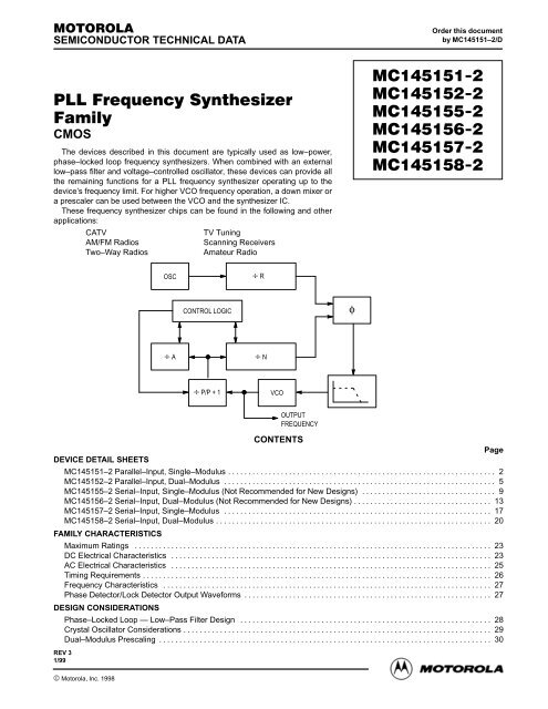
PLL Frequency Synthesizer Family MC145151-2 MC145152-2 ...
PLL Frequency Synthesizer Family MC145151-2 MC145152-2 ...
PLL Frequency Synthesizer Family MC145151-2 MC145152-2 ...

You also want an ePaper? Increase the reach of your titles
YUMPU automatically turns print PDFs into web optimized ePapers that Google loves.
SEMICONDUCTOR TECHNICAL DATA Interfaces with Single–Modulus PrescalersThe <strong>MC145151</strong>–2 is programmed by 14 parallel–input data lines for theN counter and three input lines for the R counter. The device features consist ofa reference oscillator, selectable–reference divider, digital–phase detector, and14–bit programmable divide–by–N counter.The <strong>MC145151</strong>–2 is an improved–performance drop–in replacement for the<strong>MC145151</strong>–1. The power consumption has decreased and ESD and latch–upperformance have improved.• Operating Temperature Range: – 40 to 85°C• Low Power Consumption Through Use of CMOS Technology• 3.0 to 9.0 V Supply Range• On– or Off–Chip Reference Oscillator Operation• Lock Detect Signal• ÷ N Counter Output Available• Single Modulus/Parallel Programming• 8 User–Selectable ÷ R Values: 8, 128, 256, 512, 1024, 2048, 2410, 8192• ÷ N Range = 3 to 16383• “Linearized” Digital Phase Detector Enhances Transfer Function Linearity• Two Error Signal Options: Single–Ended (Three–State) or Double–Ended• Chip Complexity: 8000 FETs or 2000 Equivalent Gates282811P SUFFIXPLASTIC DIPCASE 710DW SUFFIXSOG PACKAGECASE 751FORDERING INFORMATION<strong>MC145151</strong>P2 Plastic DIP<strong>MC145151</strong>DW2 SOG PackageVDDPDoutPIN ASSIGNMENTfinVSSRA0RA1RA2φRφVfVN0N1N2N312345678910111213142827262524232221201918171615LDOSCinOSCoutN11N10N13N12T/RN9N8N7N6N5N4REV 18/95© <strong>MC145151</strong>–2 Motorola, Inc. 1995 through MC145158–22MOTOROLA
<strong>MC145151</strong>–2 BLOCK DIAGRAMOSCoutRA2RA1RA014 x 8 ROM REFERENCE DECODER14LOCKDETECTLDOSCin14–BIT ÷ R COUNTERPHASEDETECTORAPDoutfin14–BIT ÷ N COUNTERT/RVDD14TRANSMIT OFFSET ADDERPHASEDETECTORBφVφRfVN13 N11 N9 N7 N6 N4 N2 N0NOTE: N0 – N13 inputs and inputs RA0, RA1, and RA2 have pull–up resistors that are not shown.INPUT PINSPIN DESCRIPTIONSfin<strong>Frequency</strong> Input (Pin 1)Input to the ÷ N portion of the synthesizer. fin is typicallyderived from loop VCO and is ac coupled into the device. Forlarger amplitude signals (standard CMOS logic levels) dccoupling may be used.RA0 – RA2Reference Address Inputs (Pins 5, 6, 7)These three inputs establish a code defining one of eightpossible divide values for the total reference divider, asdefined by the table below.Pull–up resistors ensure that inputs left open remain at alogic 1 and require only a SPST switch to alter data to thezero state.Reference Address CodeRA2 RA1 RA0000011110011001101010101TotalDivideValue81282565121024204824108192N0 – N11N Counter Programming Inputs (Pins 11 – 20, 22 – 25)These inputs provide the data that is preset into the ÷ Ncounter when it reaches the count of zero. N0 is the least significantand N13 is the most significant. Pull–up resistors ensurethat inputs left open remain at a logic 1 and require onlyan SPST switch to alter data to the zero state.T/RTransmit/Receive Offset Adder Input (Pin 21)This input controls the offset added to the data provided atthe N inputs. This is normally used for offsetting the VCOfrequency by an amount equal to the IF frequency of thetransceiver. This offset is fixed at 856 when T/R is low andgives no offset when T/R is high. A pull–up resistor ensuresthat no connection will appear as a logic 1 causing no offsetaddition.OSCin, OSCoutReference Oscillator Input/Output (Pins 27, 26)These pins form an on–chip reference oscillator when connectedto terminals of an external parallel resonant crystal.<strong>Frequency</strong> setting capacitors of appropriate value must beconnected from OSCin to ground and OSCout to ground.OSCin may also serve as the input for an externally–generatedreference signal. This signal is typically ac coupled toOSCin, but for larger amplitude signals (standard CMOSlogic levels) dc coupling may also be used. In the externalreference mode, no connection is required to OSCout.OUTPUT PINSPDoutPhase Detector A Output (Pin 4)Three–state output of phase detector for use as loop–errorsignal. Double–ended outputs are also available for this purpose(see φV and φR).<strong>Frequency</strong> fV > fR or fV Leading: Negative Pulses<strong>Frequency</strong> fV < fR or fV Lagging: Positive Pulses<strong>Frequency</strong> fV = fR and Phase Coincidence: High–ImpedanceStateMOTOROLA<strong>MC145151</strong>–2 through MC145158–23
φR, φVPhase Detector B Outputs (Pins 8, 9)These phase detector outputs can be combined externallyfor a loop–error signal. A single–ended output is also availablefor this purpose (see PDout).If frequency fV is greater than fR or if the phase of fV isleading, then error information is provided by φV pulsing low.φR remains essentially high.If the frequency fV is less than fR or if the phase of fV islagging, then error information is provided by φR pulsing low.φV remains essentially high.If the frequency of fV = fR and both are in phase, then bothφV and φR remain high except for a small minimum timeperiod when both pulse low in phase.fVN Counter Output (Pin 10)This is the buffered output of the ÷ N counter that is internallyconnected to the phase detector input. With this outputavailable, the ÷ N counter can be used independently.LDLock Detector Output (Pin 28)Essentially a high level when loop is locked (fR, fV of samephase and frequency). Pulses low when loop is out of lock.POWER SUPPLYVDDPositive Power Supply (Pin 3)The positive power supply potential. This pin may rangefrom + 3 to + 9 V with respect to VSS.VSSNegative Power Supply (Pin 2)The most negative supply potential. This pin is usuallyground.TYPICAL APPLICATIONS2.048 MHzNCNCOSCinN13 N12 N11OSCoutN10 N9N8fin<strong>MC145151</strong>–2N7 N6 N5RA2 RA1N4 N3 N2RA0PDoutN1 N0VOLTAGECONTROLLEDOSCILLATOR5 – 5.5 MHz0 1 1 1 0 0 0 1 0 0 0 = 5 MHz1 0 1 0 1 1 1 1 1 0 0 = 5.5 MHzREF. OSC.10.0417 MHz(ON–CHIP OSC.OPTIONAL)RECEIVE+ VFigure 1. 5 MHz to 5.5 MHz Local Oscillator Channel Spacing = 1 kHzOSCinVDDVSST/RTRANSMIT(ADDS 856 TO÷ N VALUE)OSCout“0” “0” “1”“1”RA2“1”RA1“0”RA0<strong>MC145151</strong>–2CHANNEL PROGRAMMING÷ N = 2284 TO 3484LOCK DETECT SIGNALCHOICE OFDETECTORERRORSIGNALSLOOPFILTERT: 13.0833 – 18.0833 MHzR: 9.5167 – 14.5167 MHz60.2500 MHzNOTES:1. fR = 4.1667 kHz; ÷ R = 2410; 21.4 MHz low side injection during receive.2. <strong>Frequency</strong> values shown are for the 440 – 470 MHz band. Similar implementation applies to the 406 – 440 MHz band.For 470 – 512 MHz, consider reference oscillator frequency X9 for mixer injection signal (90.3750 MHz).LDFigure 2. <strong>Synthesizer</strong> for Land Mobile Radio UHF BandsfVPDoutφRfVfinX6VCODOWNMIXERTRANSMIT: 440.0 – 470.0 MHzRECEIVE: 418.6 – 448.6 MHz(25 kHz STEPS)X6T: 73.3333 – 78.3333 MHzR: 69.7667 – 74.7667 MHz<strong>MC145151</strong>–2 Data Sheet Continued on Page 23<strong>MC145151</strong>–2 through MC145158–24MOTOROLA
SEMICONDUCTOR TECHNICAL DATA Interfaces with Dual–Modulus PrescalersThe <strong>MC145152</strong>–2 is programmed by sixteen parallel inputs for the N and Acounters and three input lines for the R counter. The device features consist ofa reference oscillator, selectable–reference divider, two–output phase detector,10–bit programmable divide–by–N counter, and 6–bit programmable ÷ Acounter.The <strong>MC145152</strong>–2 is an improved–performance drop–in replacement for the<strong>MC145152</strong>–1. Power consumption has decreased and ESD and latch–upperformance have improved.• Operating Temperature Range: – 40 to 85°C• Low Power Consumption Through Use of CMOS Technology• 3.0 to 9.0 V Supply Range• On– or Off–Chip Reference Oscillator Operation• Lock Detect Signal• Dual Modulus/Parallel Programming• 8 User–Selectable ÷ R Values: 8, 64, 128, 256, 512, 1024, 1160, 2048• ÷ N Range = 3 to 1023, ÷ A Range = 0 to 63• Chip Complexity: 8000 FETs or 2000 Equivalent Gates• See Application Note AN980282811P SUFFIXPLASTIC DIPCASE 710DW SUFFIXSOG PACKAGECASE 751FORDERING INFORMATION<strong>MC145152</strong>P2 Plastic DIP<strong>MC145152</strong>DW2 SOG PackageVDDPIN ASSIGNMENTfinVSSRA0RA1RA2φRφVMCA5N0N1N2N312345678910111213142827262524232221201918171615LDOSCinOSCoutA4A3A0A2A1N9N8N7N6N5N4REV 18/95© Motorola, Inc. 1995MOTOROLA<strong>MC145151</strong>–2 through MC145158–25
<strong>MC145152</strong>–2 BLOCK DIAGRAMOSCoutRA2RA1RA012 x 8 ROM REFERENCE DECODER12OSCin12–BIT ÷ R COUNTERLOCKDETECTLDMCCONTROLLOGICPHASEDETECTORφVφRfin6–BIT ÷ A COUNTER10–BIT ÷ N COUNTERA5 A3 A2 A0N0 N2 N4 N5 N7 N9NOTE: N0 – N9, A0 – A5, and RA0 – RA2 have pull–up resistors that are not shown.INPUT PINSPIN DESCRIPTIONSfin<strong>Frequency</strong> Input (Pin 1)Input to the positive edge triggered ÷ N and ÷ A counters.fin is typically derived from a dual–modulus prescaler and isac coupled into the device. For larger amplitude signals(standard CMOS logic levels) dc coupling may be used.RA0, RA1, RA2Reference Address Inputs (Pins 4, 5, 6)These three inputs establish a code defining one of eightpossible divide values for the total reference divider. Thetotal reference divide values are as follows:Reference Address CodeRA2 RA1 RA0000011110011001101010101TotalDivideValue864128256512102411602048N0 – N9N Counter Programming Inputs (Pins 11 – 20)The N inputs provide the data that is preset into the ÷ Ncounter when it reaches the count of 0. N0 is the least significantdigit and N9 is the most significant. Pull–up resistors ensurethat inputs left open remain at a logic 1 and require onlya SPST switch to alter data to the zero state.A0 – A5A Counter Programming Inputs(Pins 23, 21, 22, 24, 25, 10)The A inputs define the number of clock cycles of fin thatrequire a logic 0 on the MC output (see Dual–ModulusPrescaling section). The A inputs all have internal pull–upresistors that ensure that inputs left open will remain at alogic 1.OSCin, OSCoutReference Oscillator Input/Output (Pins 27, 26)These pins form an on–chip reference oscillator when connectedto terminals of an external parallel resonant crystal.<strong>Frequency</strong> setting capacitors of appropriate value must beconnected from OSCin to ground and OSCout to ground.OSCin may also serve as the input for an externally–generatedreference signal. This signal is typically ac coupled toOSCin, but for larger amplitude signals (standard CMOSlogic levels) dc coupling may also be used. In the externalreference mode, no connection is required to OSCout.OUTPUT PINSφR, φVPhase Detector B Outputs (Pins 7, 8)These phase detector outputs can be combined externallyfor a loop–error signal.If the frequency fV is greater than fR or if the phase of fV isleading, then error information is provided by φV pulsing low.φR remains essentially high.If the frequency fV is less than fR or if the phase of fV islagging, then error information is provided by φR pulsing low.φV remains essentially high.If the frequency of fV = fR and both are in phase, then bothφV and φR remain high except for a small minimum timeperiod when both pulse low in phase.MCDual–Modulus Prescale Control Output (Pin 9)Signal generated by the on–chip control logic circuitry forcontrolling an external dual–modulus prescaler. The MClevel will be low at the beginning of a count cycle and willremain low until the ÷ A counter has counted down from itsprogrammed value. At this time, MC goes high and remainshigh until the ÷ N counter has counted the rest of the waydown from its programmed value (N – A additional countssince both ÷ N and ÷ A are counting down during the first<strong>MC145151</strong>–2 through MC145158–26MOTOROLA
portion of the cycle). MC is then set back low, the counterspreset to their respective programmed values, and the abovesequence repeated. This provides for a total programmabledivide value (NT)= N•P + A where P and P + 1 represent thedual–modulus prescaler divide values respectively for highand low MC levels, N the number programmed into the ÷ Ncounter, and A the number programmed into the ÷ A counter.LDLock Detector Output (Pin 28)Essentially a high level when loop is locked (fR, fV of samephase and frequency). Pulses low when loop is out of lock.POWER SUPPLYVDDPositive Power Supply (Pin 3)The positive power supply potential. This pin may rangefrom + 3 to + 9 V with respect to VSS.VSSNegative Power Supply (Pin 2)The most negative supply potential. This pin is usuallyground.NO CONNECTSTYPICAL APPLICATIONS10.24 MHzNOTE 1“1” “1” “1”LOCK DETECT SIGNALR2C150 – 175 MHz5 kHz STEPS+ VOSCinVDDVSSOSCout RA2 RA1<strong>MC145152</strong>–2RA0LDφRφVMCfinR1R1R2C–+MC33171NOTE 2VCON9N0 A5A0CHANNEL PROGRAMMINGNOTES:1. Off–chip oscillator optional.2. The φR and φV outputs are fed to an external combiner/loop filter. See the Phase–Locked Loop — Low–Pass FilterDesign page for additional information. The φR and φV outputs swing rail–to–rail. Therefore, the user should be carefulnot to exceed the common mode input range of the op amp used in the combiner/loop filter.Figure 1. <strong>Synthesizer</strong> for Land Mobile Radio VHF BandsMC12017÷ 64/65 PRESCALERMOTOROLA<strong>MC145151</strong>–2 through MC145158–27
REF. OSC.15.360 MHz(ON–CHIP OSC.OPTIONAL)X2NO CONNECTS“1” “1” “1”RECEIVER 2ND L.O.30.720 MHzLOCK DETECT SIGNALR2CRECEIVER FIRST L.O.825.030 844.980 MHz(30 kHz STEPS)+ VOSCinVDDVSSN9OSCout RA2 RA1<strong>MC145152</strong>–2NOTE 5N0 A5RA0LDφRφVMCfinA0R1R1R2C–+NOTE 7VCOX4NOTE 6TRANSMITTERMODULATIONX4NOTE 6CHANNEL PROGRAMMINGMC12017÷ 64/65 PRESCALERNOTE 6NOTES:1. Receiver 1st I.F. = 45 MHz, low side injection; Receiver 2nd I.F. = 11.7 MHz, low side injection.2. Duplex operation with 45 MHz receiver/transmit separation.3. fR = 7.5 kHz; ÷ R = 2048.4. Ntotal = N 64 + A = 27501 to 28166; N = 429 to 440; A = 0 to 63.5. MC145158–2 may be used where serial data entry is desired.6. High frequency prescalers (e.g., MC12018 [520 MHz] and MC12022 [1 GHz]) may be used for higher frequency VCO and frefimplementations.7. The φR and φV outputs are fed to an external combiner/loop filter. See the Phase–Locked Loop — Low–Pass Filter Design page foradditional information. The φR and φV outputs swing rail–to–rail. Therefore, the user should be careful not to exceed the common modeinput range of the op amp used in the combiner/loop filter.Figure 2. 666–Channel, Computer–Controlled, Mobile Radiotelephone <strong>Synthesizer</strong>for 800 MHz Cellular Radio SystemsTRANSMITTER SIGNAL825.030 844.980 MHz(30 kHz STEPS)<strong>MC145152</strong>–2 Data Sheet Continued on Page 23<strong>MC145151</strong>–2 through MC145158–28MOTOROLA
SEMICONDUCTOR TECHNICAL DATA Interfaces with Single–Modulus PrescalersThe MC145155–2 is programmed by a clocked, serial input, 16–bit datastream. The device features consist of a reference oscillator, selectable–referencedivider, digital–phase detector, 14–bit programmable divide–by–Ncounter, and the necessary shift register and latch circuitry for accepting serialinput data.The MC145155–2 is an improved–performance drop–in replacement for theMC145155–1. Power consumption has decreased and ESD and latch–upperformance have improved.• Operating Temperature Range: – 40 to 85°C• Low Power Consumption Through Use of CMOS Technology• 3.0 to 9.0 V Supply Range• On– or Off–Chip Reference Oscillator Operation with Buffered Output• Compatible with the Serial Peripheral Interface (SPI) on CMOS MCUs• Lock Detect Signal• Two Open–Drain Switch Outputs• 8 User–Selectable ÷ R Values: 16, 512, 1024, 2048, 3668, 4096, 6144,8192• Single Modulus/Serial Programming• ÷ N Range = 3 to 16383• “Linearized” Digital Phase Detector Enhances Transfer Function Linearity• Two Error Signal Options: Single–Ended (Three–State) or Double–Ended• Chip Complexity: 6504 FETs or 1626 Equivalent GatesNOT RECOMMENDED FOR NEW DESIGNS;PRODUCT TO BE PHASED OUT.Closest equivalents are the MC145157–2, MC145170–2,MC14519X series, and MC14520X series.182011P SUFFIXPLASTIC DIPCASE 707DW SUFFIXSOG PACKAGECASE 751DORDERING INFORMATIONMC145155P2 Plastic DIPMC145155DW2 SOG PackagePIN ASSIGNMENTSRA1RA2φVφRVDDPDoutVSSLDfinPLASTIC DIP123456789181716151413121110RA0OSCinOSCoutREFoutSW2SW1ENBDATACLKSOG PACKAGERA1RA212φV 3φR 4VDD 5PDout 6VSS 7NC 8LD 9fin 1020191817161514131211RA0OSCinOSCoutREFoutNCSW2SW1ENBDATACLKNC = NO CONNECTIONREV 31/99© Motorola, Inc. 1998MOTOROLA<strong>MC145151</strong>–2 through MC145158–29
MC145155–2 BLOCK DIAGRAMOSCoutRA2RA1RA014 x 8 ROM REFERENCE DECODER14LOCKDETECTLDOSCin14–BIT ÷ R COUNTERREFoutfRfVPHASEDETECTORAPDoutfin14–BIT ÷ N COUNTERVDD14PHASEDETECTORBφVφRSW2ENBLATCHLATCHSW1DATACLK1414–BIT SHIFT REGISTER2–BIT SHIFTREGISTERINPUT PINSPIN DESCRIPTIONSfin<strong>Frequency</strong> Input (PDIP – Pin 9, SOG – Pin 10)Input to the ÷ N portion of the synthesizer. fin is typicallyderived from loop VCO and is ac coupled into the device. Forlarger amplitude signals (standard CMOS logic levels) dccoupling may be used.RA0, RA1, RA2Reference Address Inputs (PDIP – Pins 18, 1, 2;SOG – Pins 20, 1, 2)These three inputs establish a code defining one of eightpossible divide values for the total reference divider, asdefined by the table below:Reference Address CodeRA2 RA1 RA0000011110011001101010101TotalDivideValue16512102420483668409661448192CLK, DATAShift Register Clock, Serial Data Inputs(PDIP – Pins 10, 11; SOG – Pins 11, 12)Each low–to–high transition clocks one bit into the on–chip16–bit shift register. The Data input provides programminginformation for the 14–bit ÷ N counter and the two switch signalsSW1 and SW2. The entry format is as follows:N LSB÷÷ N COUNTER BITSN MSB÷LAST DATA BIT IN (BIT NO. 16)FIRST DATA BIT IN (BIT NO. 1)SW2SW1ENBLatch Enable Input (PDIP – Pin 12, SOG – Pin 13)When high (1), ENB transfers the contents of the shift registerinto the latches, and to the programmable counter inputs,and the switch outputs SW1 and SW2. When low (0),ENB inhibits the above action and thus allows changes to bemade in the shift register data without affecting the counterprogramming and switch outputs. An on–chip pull–up establishesa continuously high level for ENB when no externalsignal is applied. ENB is normally low and is pulsed high totransfer data to the latches.OSCin, OSCoutReference Oscillator Input/Output (PDIP – Pins 17, 16;SOG – Pins 19, 18)These pins form an on–chip reference oscillator when connectedto terminals of an external parallel resonant crystal.<strong>Frequency</strong> setting capacitors of appropriate value must beconnected from OSCin to ground and OSCout to ground.OSCin may also serve as the input for an externally–generatedreference signal. This signal is typically ac coupled toOSCin, but for larger amplitude signals (standard CMOSlogic levels) dc coupling may also be used. In the externalreference mode, no connection is required to OSCout.<strong>MC145151</strong>–2 through MC145158–210MOTOROLA
OUTPUT PINSPDoutPhase Detector A Output (PDIP, SOG – Pin 6)Three–state output of phase detector for use as loop errorsignal. Double–ended outputs are also available for this purpose(see φV and φR).<strong>Frequency</strong> fV > fR or fV Leading: Negative Pulses<strong>Frequency</strong> fV < fR or fV Lagging: Positive Pulses<strong>Frequency</strong> fV = fR and Phase Coincidence: High–ImpedanceStateφR, φVPhase Detector B Outputs (PDIP, SOG – Pins 4, 3)These phase detector outputs can be combined externallyfor a loop–error signal. A single–ended output is also availablefor this purpose (see PDout).If frequency fV is greater than fR or if the phase of fV isleading, then error information is provided by φV pulsing low.φR remains essentially high.If the frequency fV is less than fR or if the phase of fV islagging, then error information is provided by φR pulsing low.φV remains essentially high.If the frequency of fV = fR and both are in phase, then bothφV and φR remain high except for a small minimum timeperiod when both pulse low in phase.LDLock Detector Output (PDIP – Pin 8, SOG – Pin 9)Essentially a high level when loop is locked (fR, fV of samephase and frequency). LD pulses low when loop is out oflock.SW1, SW2Band Switch Outputs (PDIP – Pins 13, 14;SOG – Pins 14, 15)SW1 and SW2 provide latched open–drain outputs correspondingto data bits numbers one and two. These outputscan be tied through external resistors to voltages as high as15 V, independent of the VDD supply voltage. These aretypically used for band switch functions. A logic 1 causes theoutput to assume a high–impedance state, while a logic 0causes the output to be low.REFoutBuffered Reference Oscillator Output (PDIP, SOG –Pin 15)Buffered output of on–chip reference oscillator or externallyprovided reference–input signal.POWER SUPPLYVDDPositive Power Supply (PDIP, SOG – Pin 5)The positive power supply potential. This pin may rangefrom + 3 to + 9 V with respect to VSS.VSSNegative Power Supply (PDIP, SOG – Pin 7)The most negative supply potential. This pin is usuallyground.TYPICAL APPLICATIONSUHF/VHFTUNER ORCATVFRONT ENDMC12073/74PRESCALERfin4.0 MHzMC145155–2φRφV–+1/2 MC1458*DATACLKENBKEYBOARDCMOSMPU/MCU3MC14489LED DISPLAY* The φR and φV outputs are fed to an external combiner/loop filter. See the Phase–Locked Loop — Low–Pass Filter Design pagefor additional information. The φR and φV outputs swing rail–to–rail. Therefore, the user should be careful not to exceed the commonmode input range of the op amp used in the combiner/loop filter.Figure 1. Microprocessor–Controlled TV/CATV Tuning System with Serial InterfaceMOTOROLA<strong>MC145151</strong>–2 through MC145158–211
2.56 MHzFMOSCMC12019÷ 20 PRESCALERfinMC145155–2φRφV–+1/2 MC1458*TOAM/FMOSCILLATORSAMOSCDATACLKENBKEYBOARDCMOSMPU/MCUTO DISPLAY* The φR and φV outputs are fed to an external combiner/loop filter. See the Phase–Locked Loop — Low–Pass Filter Design pagefor additional information. The φR and φV outputs swing rail–to–rail. Therefore, the user should be careful not to exceed the commonmode input range of the op amp used in the combiner/loop filter.Figure 2. AM/FM Radio <strong>Synthesizer</strong>MC145155–2 Data Sheet Continued on Page 23<strong>MC145151</strong>–2 through MC145158–212MOTOROLA
SEMICONDUCTOR TECHNICAL DATA Interfaces with Dual–Modulus PrescalersThe MC145156–2 is programmed by a clocked, serial input, 19–bit datastream. The device features consist of a reference oscillator, selectable–referencedivider, digital–phase detector, 10–bit programmable divide–by–Ncounter, 7–bit programmable divide–by–A counter, and the necessary shiftregister and latch circuitry for accepting serial input data.The MC145156–2 is an improved–performance drop–in replacement for theMC145156–1. Power consumption has decreased and ESD and latch–upperformance have improved.• Operating Temperature Range: – 40 to 85°C• Low Power Consumption Through Use of CMOS Technology• 3.0 to 9.0 V Supply Range• On– or Off–Chip Reference Oscillator Operation with Buffered Output• Compatible with the Serial Peripheral Interface (SPI) on CMOS MCUs• Lock Detect Signal• Two Open–Drain Switch Outputs• Dual Modulus/Serial Programming• 8 User–Selectable ÷ R Values: 8, 64, 128, 256, 640, 1000, 1024, 2048• ÷ N Range = 3 to 1023, ÷ A Range = 0 to 127• “Linearized” Digital Phase Detector Enhances Transfer Function Linearity• Two Error Signal Options: Single–Ended (Three–State) or Double–Ended• Chip Complexity: 6504 FETs or 1626 Equivalent GatesNOT RECOMMENDED FOR NEW DESIGNS;PRODUCT TO BE PHASED OUT.Closest equivalents are the MC145158–2, MC145170–2,MC14519X series, and MC14520X series.202011P SUFFIXPLASTIC DIPCASE 738DW SUFFIXSOG PACKAGECASE 751DORDERING INFORMATIONMC145156P2 Plastic DIPMC145156DW2 SOG PackagePDoutPIN ASSIGNMENTRA1RA2φVφRVDD 5VSSMCLDfin123467891020191817161514131211RA0OSCinOSCoutREFoutTESTSW2SW1ENBDATACLKREV 31/99© Motorola, Inc. 1998MOTOROLA<strong>MC145151</strong>–2 through MC145158–213
MC145156–2 BLOCK DIAGRAMRA2RA1RA012 x 8 ROM REFERENCE DECODER12OSCin12–BIT ÷ R COUNTERLOCKDETECTLDOSCoutREFoutMCCONTROL LOGICfRfVPHASEDETECTORAPDoutfinVDD7–BIT ÷ A COUNTER710–BIT ÷ N COUNTERPHASEDETECTORBφVφR10 SW2ENB÷ A COUNTER LATCH ÷ N COUNTER LATCHLATCHSW1DATACLK7–BIT SHIFT REGISTER71010–BIT SHIFT REGISTER2–BIT SHIFTREGISTERINPUT PINSPIN DESCRIPTIONSfin<strong>Frequency</strong> Input (Pin 10)Input to the positive edge triggered ÷ N and ÷ A counters.fin is typically derived from a dual–modulus prescaler and isac coupled into the device. For larger amplitude signals(standard CMOS logic levels), dc coupling may be used.RA0, RA1, RA2Reference Address Inputs (Pins 20, 1, 2)These three inputs establish a code defining one of eightpossible divide values for the total reference divider, asdefined by the table below:Reference Address CodeRA2 RA1 RA0000011110011001101010101TotalDivideValue864128256640100010242048CLK, DATAShift Register Clock, Serial Data Inputs (Pins 11, 12)Each low–to–high transition clocks one bit into the on–chip19–bit shift register. The data input provides programming informationfor the 10–bit ÷ N counter, the 7–bit ÷ A counter,and the two switch signals SW1 and SW2. The entry formatis as follows:A LSB÷÷ A COUNTER BITSA MSBN LSB÷÷÷ N COUNTER BITSLAST DATA BIT IN (BIT NO. 19)FIRST DATA BIT IN (BIT NO. 1)N MSBSW2SW1÷ENBLatch Enable Input (Pin 13)When high (1), ENB transfers the contents of the shift registerinto the latches, and to the programmable counter inputs,and the switch outputs SW1 and SW2. When low (0),ENB inhibits the above action and thus allows changes to bemade in the shift register data without affecting the counterprogramming and switch outputs. An on–chip pull–up establishesa continuously high level for ENB when no externalsignal is applied. ENB is normally low and is pulsed high totransfer data to the latches.OSCin, OSCoutReference Oscillator Input/Output (Pins 19, 18)These pins form an on–chip reference oscillator when connectedto terminals of an external parallel resonant crystal.<strong>Frequency</strong> setting capacitors of appropriate value must beconnected from OSCin to ground and OSCout to ground.OSCin may also serve as the input for an externally–generatedreference signal. This signal is typically ac coupled toOSCin, but for larger amplitude signals (standard CMOSlogic levels) dc coupling may also be used. In the externalreference mode, no connection is required to OSCout.TESTFactory Test Input (Pin 16)Used in manufacturing. Must be left open or tied to VSS.<strong>MC145151</strong>–2 through MC145158–214MOTOROLA
OUTPUT PINSPDoutPhase Detector A Output (Pin 6)Three–state output of phase detector for use as loop–errorsignal. Double–ended outputs are also available for this purpose(see φV and φR).<strong>Frequency</strong> fV > fR or fV Leading: Negative Pulses<strong>Frequency</strong> fV < fR or fV Lagging: Positive Pulses<strong>Frequency</strong> fV = fR and Phase Coincidence: High–ImpedanceStateφR, φVPhase Detector B Outputs (Pins 4, 3)These phase detector outputs can be combined externallyfor a loop–error signal. A single–ended output is also availablefor this purpose (see PDout).If frequency fV is greater than fR or if the phase of fV isleading, then error information is provided by φV pulsing low.φR remains essentially high.If the frequency fV is less than fR or if the phase of fV islagging, then error information is provided by φR pulsing low.φV remains essentially high.If the frequency of fV = fR and both are in phase, then bothφV and φR remain high except for a small minimum timeperiod when both pulse low in phase.MCDual–Modulus Prescale Control Output (Pin 8)Signal generated by the on–chip control logic circuitry forcontrolling an external dual–modulus prescaler. The MClevel will be low at the beginning of a count cycle and willremain low until the ÷ A counter has counted down from itsprogrammed value. At this time, MC goes high and remainshigh until the ÷ N counter has counted the rest of the waydown from its programmed value (N – A additional countssince both ÷ N and ÷ A are counting down during the first portionof the cycle). MC is then set back low, the counterspreset to their respective programmed values, and the abovesequence repeated. This provides for a total programmabledivide value (NT) = N P + A where P and P + 1 represent thedual–modulus prescaler divide values respectively for highand low MC levels, N the number programmed into the ÷ Ncounter, and A the number programmed into the ÷ A counter.LDLock Detector Output (Pin 9)Essentially a high level when loop is locked (fR, fV of samephase and frequency). LD pulses low when loop is out oflock.SW1, SW2Band Switch Outputs (Pins 14, 15)SW1 and SW2 provide latched open–drain outputs correspondingto data bits numbers one and two. These outputscan be tied through external resistors to voltages as high as15 V, independent of the VDD supply voltage. These aretypically used for band switch functions. A logic 1 causes theoutput to assume a high–impedance state, while a logic 0causes the output to be low.REFoutBuffered Reference Oscillator Output (Pin 17)Buffered output of on–chip reference oscillator or externallyprovided reference–input signal.POWER SUPPLYVDDPositive Power Supply (Pin 5)The positive power supply potential. This pin may rangefrom + 3 to + 9 V with respect to VSS.VSSNegative Power Supply (Pin 7)The most negative supply potential. This pin is usuallyground.MOTOROLA<strong>MC145151</strong>–2 through MC145158–215
3.2 MHzTYPICAL APPLICATIONSLOCK DETECT SIGNAL+ 12 VNOTES 1AND 2+ 12 V FM B ++ VOSCinVDDVSSREFoutCLKOSCoutDATARA2 RA1 RA0MC145156–2ENB finLDSW1 SW2PDoutφRφVMCOPTIONALLOOPERROR SIGNAL–+1/2 MC1458NOTE 3AM B +VCOKEY–BOARDCMOS MPU/MCUMC12019÷ 20/21 DUAL MODULUS PRESCALERTO DISPLAY DRIVER (e.g., MC14489)NOTES:1. For AM: channel spacing = 5 kHz, ÷ R = ÷ 640 (code 100).2. For FM: channel spacing = 25 kHz, ÷ R = ÷ 128 (code 010).3. The φR and φV outputs are fed to an external combiner/loop filter. See the Phase–Locked Loop — Low–Pass Filter Design pagefor additional information. The φR and φV outputs swing rail–to–rail. Therefore, the user should be careful not to exceed thecommon mode input range of the op amp used in the combiner/loop filter.3.2 MHz (NOTE 3)Figure 1. AM/FM Radio Broadcast <strong>Synthesizer</strong>+ VOSCinVDDVSSREFoutCLKOSCoutDATANAV = 01COM = 10RA2 RA1 RA0MC145156–2ENBfinLDLOCK DETECT SIGNALSW1 SW2PDoutφRφVMC–+VCO RANGENAV: 97.300 – 107.250 MHzCOM–T: 118.000 – 135.975 MHzCOM–R: 139.400 – 157.375 MHzMC33171NOTE 5VCOR/TCMOS MPU/MCUCHANNELSELECTIONTO DISPLAY DRIVER(e.g., MC14489)MC12016 (NOTES 2 AND 4)÷ 40/41 DUAL MODULUS PRESCALERNOTES:1. For NAV: fR = 50 kHz, ÷ R = 64 using 10.7 MHz lowside injection, Ntotal = 1946 – 2145.For COM–T: fR = 25 kHz, ÷ R = 128, Ntotal = 4720 – 5439.For COM–R: fR = 25 kHz, ÷ R = 128, using 21.4 MHz highside injection, Ntotal = 5576 – 6295.2. A ÷ 32/33 dual modulus approach is provided by substituting an MC12015 for the MC12016. The devices are pin equivalent.3. A 6.4 MHz oscillator crystal can be used by selecting ÷ R = 128 (code 010) for NAV and ÷ R = 256 (code 011) for COM.4. MC12013 + MC10131 combination may also be used to form the ÷ 40/41 prescaler.5. The φR and φV outputs are fed to an external combiner/loop filter. See the Phase–Locked Loop — Low–Pass Filter Designpage for additional information. The φR and φV outputs swing rail–to–rail. Therefore, the user should be careful not to exceedthe common mode input range of the op amp used in the combiner/loop filter.Figure 2. Avionics Navigation or Communication <strong>Synthesizer</strong>MC145156–2 Data Sheet Continued on Page 23<strong>MC145151</strong>–2 through MC145158–216MOTOROLA
SEMICONDUCTOR TECHNICAL DATA Interfaces with Single–Modulus PrescalersThe MC145157–2 has a fully programmable 14–bit reference counter, as wellas a fully programmable ÷ N counter. The counters are programmed seriallythrough a common data input and latched into the appropriate counter latch,according to the last data bit (control bit) entered.The MC145157–2 is an improved–performance drop–in replacement for theMC145157–1. Power consumption has decreased and ESD and latch–upperformance have improved.• Operating Temperature Range: – 40 to 85°C• Low Power Consumption Through Use of CMOS Technology• 3.0 to 9.0 V Supply Range• Fully Programmable Reference and ÷ N Counters• ÷ R Range = 3 to 16383• ÷ N Range = 3 to 16383• fV and fR Outputs• Lock Detect Signal• Compatible with the Serial Peripheral Interface (SPI) on CMOS MCUs• “Linearized” Digital Phase Detector• Single–Ended (Three–State) or Double–Ended Phase Detector Outputs• Chip Complexity: 6504 FETs or 1626 Equivalent Gates161611P SUFFIXPLASTIC DIPCASE 648DW SUFFIXSOG PACKAGECASE 751GORDERING INFORMATIONMC145157P2 Plastic DIPMC145157DW2 SOG PackageOSCinOSCoutPIN ASSIGNMENTfVVDDPDoutVSSLDfin12345678161514131211109φRφVREFoutfRS/RoutENBDATACLKREV 18/95© Motorola, Inc. 1995MOTOROLA<strong>MC145151</strong>–2 through MC145158–217
MC145157–2 BLOCK DIAGRAM14–BIT SHIFT REGISTERENB14REFERENCE COUNTER LATCH14LOCKDETECTfRLDOSCin14–BIT ÷ R COUNTEROSCoutREFoutPHASEDETECTORAPDoutfin14–BIT ÷ N COUNTER14PHASEDETECTORBφVφR÷ N COUNTER LATCHfVDATA1–BITCONTROLS/R1414–BIT SHIFT REGISTERS/RoutCLKINPUT PINSPIN DESCRIPTIONSfin<strong>Frequency</strong> Input (Pin 8)Input frequency from VCO output. A rising edge signal onthis input decrements the ÷ N counter. This input has aninverter biased in the linear region to allow use with accoupled signals as low as 500 mV p–p. For larger amplitudesignals (standard CMOS logic levels), dc coupling may beused.CLK, DATAShift Clock, Serial Data Inputs (Pins 9, 10)Each low–to–high transition of the clock shifts one bit ofdata into the on–chip shift registers. The last data bit entereddetermines which counter storage latch is activated; a logic 1selects the reference counter latch and a logic 0 selects the÷ N counter latch. The entry format is as follows:CONTROLLSBFIRST DATA BIT INTO SHIFT REGISTERENBLatch Enable Input (Pin 11)A logic high on this pin latches the data from the shift registerinto the reference divider or ÷ N latches depending on thecontrol bit. The reference divider latches are activated if thecontrol bit is at a logic high and the ÷ N latches are activatedMSBif the control bit is at a logic low. A logic low on this pin allowsthe user to change the data in the shift registers withoutaffecting the counters. ENB is normally low and is pulsedhigh to transfer data to the latches.OSCin, OSCoutReference Oscillator Input/Output (Pins 1, 2)These pins form an on–chip reference oscillator when connectedto terminals of an external parallel resonant crystal.<strong>Frequency</strong> setting capacitors of appropriate value must beconnected from OSCin to ground and OSCout to ground.OSCin may also serve as the input for an externally–generatedreference signal. This signal is typically ac coupled toOSCin, but for larger amplitude signals (standard CMOSlogic levels) dc coupling may also be used. In the externalreference mode, no connection is required to OSCout.OUTPUT PINSPDoutSingle–Ended Phase Detector A Output (Pin 5)This single–ended (three–state) phase detector outputproduces a loop–error signal that is used with a loop filter tocontrol a VCO.<strong>Frequency</strong> fV > fR or fV Leading: Negative Pulses<strong>Frequency</strong> fV < fR or fV Lagging: Positive Pulses<strong>Frequency</strong> fV = fR and Phase Coincidence: High–ImpedanceStateφR, φVDouble–Ended Phase Detector B Outputs (Pins 16, 15)These outputs can be combined externally for a loop–errorsignal. A single–ended output is also available for this purpose(see PDout).<strong>MC145151</strong>–2 through MC145158–218MOTOROLA
If frequency fV is greater than fR or if the phase of fV isleading, then error information is provided by φV pulsing low.φR remains essentially high.If the frequency fV is less than fR or if the phase of fV islagging, then error information is provided by φR pulsing low.φV remains essentially high.If the frequency of fV = fR and both are in phase, then bothφV and φR remain high except for a small minimum timeperiod when both pulse low in phase.fR, fVR Counter Output, N Counter Output (Pins 13, 3)Buffered, divided reference and fin frequency outputs. ThefR and fV outputs are connected internally to the ÷ R and ÷ Ncounter outputs respectively, allowing the counters to beused independently, as well as monitoring the phase detectorinputs.LDLock Detector Output (Pin 7)This output is essentially at a high level when the loop islocked (fR, fV of same phase and frequency), and pulses lowwhen loop is out of lock.REFoutBuffered Reference Oscillator Output (Pin 14)This output can be used as a second local oscillator, referenceoscillator to another frequency synthesizer, or as thesystem clock to a microprocessor controller.S/RoutShift Register Output (Pin 12)This output can be connected to an external shift registerto provide band switching, control information, and counterprogramming code checking.POWER SUPPLYVDDPositive Power Supply (Pin 4)The positive power supply potential. This pin may rangefrom + 3 to + 9 V with respect to VSS.VSSNegative Power Supply (Pin 6)The most negative supply potential. This pin is usuallyground.MC145157–2 Data Sheet Continued on Page 23MOTOROLA<strong>MC145151</strong>–2 through MC145158–219
SEMICONDUCTOR TECHNICAL DATA Interfaces with Dual–Modulus PrescalersThe MC145158–2 has a fully programmable 14–bit reference counter, as wellas fully programmable ÷ N and ÷ A counters. The counters are programmedserially through a common data input and latched into the appropriate counterlatch, according to the last data bit (control bit) entered.The MC145158–2 is an improved–performance drop–in replacement for theMC145158–1. Power consumption has decreased and ESD and latch–upperformance have improved.• Operating Temperature Range: – 40 to 85°C• Low Power Consumption Through Use of CMOS Technology• 3.0 to 9.0 V Supply Range• Fully Programmable Reference and ÷ N Counters• ÷ R Range = 3 to 16383• ÷ N Range = 3 to 1023• Dual Modulus Capability; ÷ A Range = 0 to 127• fV and fR Outputs• Lock Detect Signal• Compatible with the Serial Peripheral Interface (SPI) on CMOS MCUs• “Linearized” Digital Phase Detector• Single–Ended (Three–State) or Double–Ended Phase Detector Outputs• Chip Complexity: 6504 FETs or 1626 Equivalent Gates161611P SUFFIXPLASTIC DIPCASE 648DW SUFFIXSOG PACKAGECASE 751GORDERING INFORMATIONMC145158P2 Plastic DIPMC145158DW2 SOG PackageOSCinOSCoutPIN ASSIGNMENTfVVDDPDoutVSSLDfin12345678161514131211109φRφVREFoutfRMCENBDATACLKREV 18/95© <strong>MC145151</strong>–2 Motorola, Inc. 1995 through MC145158–220MOTOROLA
MC145158–2 BLOCK DIAGRAM14–BIT SHIFT REGISTERENB14REFERENCE COUNTER LATCH14LOCKDETECTfRLDOSCin14–BIT ÷ R COUNTEROSCoutREFoutCONTROL LOGICPHASEDETECTORAPDoutfin7–BIT ÷ ACOUNTER7÷ A COUNTERLATCH10–BIT ÷ NCOUNTER10÷ N COUNTERLATCHPHASEDETECTORBφVφRfVDATA1–BITCONTROLS/R77–BIT S/R1010–BIT S/RMCCLKPIN DESCRIPTIONS÷ A÷ NINPUT PINSfin<strong>Frequency</strong> Input (Pin 8)Input frequency from VCO output. A rising edge signal onthis input decrements the ÷ A and ÷ N counters. This inputhas an inverter biased in the linear region to allow use withac coupled signals as low as 500 mV p–p. For larger amplitudesignals (standard CMOS logic levels), dc coupling maybe used.CLK, DATAShift Clock, Serial Data Inputs (Pins 9, 10)Each low–to–high transition of the CLK shifts one bit ofdata into the on–chip shift registers. The last data bit entereddetermines which counter storage latch is activated; a logic 1selects the reference counter latch and a logic 0 selects the÷ A, ÷ N counter latch. The data entry format is as follows:CONTROLLSB÷ RFIRST DATA BIT INTO SHIFT REGISTERMSBCONTROLLSBMSBLSBFIRST DATA BIT INTO SHIFT REGISTERENBLatch Enable Input (Pin 11)A logic high on this pin latches the data from the shift registerinto the reference divider or ÷ N, ÷ A latches depending onthe control bit. The reference divider latches are activated ifthe control bit is at a logic high and the ÷ N, ÷ A latches areactivated if the control bit is at a logic low. A logic low on thispin allows the user to change the data in the shift registerswithout affecting the counters. ENB is normally low and ispulsed high to transfer data to the latches.OSCin, OSCoutReference Oscillator Input/Output (Pins 1, 2)These pins form an on–chip reference oscillator when connectedto terminals of an external parallel resonant crystal.<strong>Frequency</strong> setting capacitors of appropriate value must beconnected from OSCin to ground and OSCout to ground.OSCin may also serve as the input for an externally–generatedreference signal. This signal is typically ac coupled toOSCin, but for larger amplitude signals (standard CMOS logiclevels) dc coupling may also be used. In the external referencemode, no connection is required to OSCout.MSBMOTOROLA<strong>MC145151</strong>–2 through MC145158–221
OUTPUT PINSPDoutPhase Detector A Output (Pin 5)This single–ended (three–state) phase detector outputproduces a loop–error signal that is used with a loop filter tocontrol a VCO.<strong>Frequency</strong> fV > fR or fV Leading: Negative Pulses<strong>Frequency</strong> fV < fR or fV Lagging: Positive Pulses<strong>Frequency</strong> fV = fR and Phase Coincidence: High–ImpedanceStateφR, φVPhase Detector B Outputs (Pins 16, 15)Double–ended phase detector outputs. These outputs canbe combined externally for a loop–error signal. A single–ended output is also available for this purpose (see PDout).If frequency fV is greater than fR or if the phase of fV isleading, then error information is provided by φV pulsing low.φR remains essentially high.If the frequency fV is less than fR or if the phase of fV islagging, then error information is provided by φR pulsing low.φV remains essentially high.If the frequency of fV = fR and both are in phase, then bothφV and φR remain high except for a small minimum timeperiod when both pulse low in phase.MCDual–Modulus Prescale Control Output (Pin 12)This output generates a signal by the on–chip control logiccircuitry for controlling an external dual–modulus prescaler.The MC level is low at the beginning of a count cycle andremains low until the ÷ A counter has counted down from itsprogrammed value. At this time, MC goes high and remainshigh until the ÷ N counter has counted the rest of the waydown from its programmed value (N – A additional countssince both ÷ N and ÷ A are counting down during the first portionof the cycle). MC is then set back low, the counters presetto their respective programmed values, and the abovesequence repeated. This provides for a total programmabledivide value (NT) = N P + A where P and P + 1 represent thedual–modulus prescaler divide values respectively for highand low modulus control levels, N the number programmedinto the ÷ N counter, and A the number programmed into the÷ A counter. Note that when a prescaler is needed, the dual–modulus version offers a distinct advantage. The dual–modulus prescaler allows a higher reference frequency atthe phase detector input, increasing system performance capability,and simplifying the loop filter design.fR, fVR Counter Output, N Counter Output (Pins 13, 3)Buffered, divided reference and fin frequency outputs. ThefR and fV outputs are connected internally to the ÷ R and÷ N counter outputs respectively, allowing the counters to beused independently, as well as monitoring the phase detectorinputs.LDLock Detector Output (Pin 7)This output is essentially at a high level when the loop islocked (fR, fV of same phase and frequency), and pulses lowwhen loop is out of lock.REFoutBuffered Reference Oscillator Output (Pin 14)This output can be used as a second local oscillator, referenceoscillator to another frequency synthesizer, or as thesystem clock to a microprocessor controller.POWER SUPPLYVDDPositive Power Supply (Pin 4)The positive power supply potential. This pin may rangefrom + 3 to + 9 V with respect to VSS.VSSNegative Power Supply (Pin 6)The most negative supply potential. This pin is usuallyground.<strong>MC145151</strong>–2 through MC145158–222MOTOROLA
MC14515X–2 FAMILY CHARACTERISTICS AND DESCRIPTIONSMAXIMUM RATINGS* (Voltages Referenced to VSS)Symbol Parameter Value UnitVDD DC Supply Voltage – 0.5 to + 10.0 VVin, VoutVoutIin, IoutInput or Output Voltage (DC or Transient)except SW1, SW2Output Voltage (DC or Transient),SW1, SW2 (Rpull–up = 4.7 kΩ)Input or Output Current (DC or Transient),per Pin– 0.5 to VDD + 0.5 V– 0.5 to + 15 V± 10 mAIDD, ISS Supply Current, VDD or VSS Pins ± 30 mAPD Power Dissipation, per Package† 500 mWTstg Storage Temperature – 65 to + 150 °CTLLead Temperature, 1 mm from Case for10 seconds260 °C* Maximum Ratings are those values beyond which damage to the device may occur.Functional operation should be restricted to the limits in the Electrical Characteristicstables or Pin Descriptions section.†Power Dissipation Temperature Derating:Plastic DIP: – 12 mW/°C from 65 to 85°CSOG Package: – 7 mW/°C from 65 to 85°CThese devices contain protection circuitry toprotect against damage due to high staticvoltages or electric fields. However, precautionsmust be taken to avoid applications of anyvoltage higher than maximum rated voltagesto these high–impedance circuits. For properoperation, Vin and Vout should be constrainedto the range VSS ≤ (Vin or Vout) ≤ VDDexcept for SW1 and SW2.SW1 and SW2 can be tied through externalresistors to voltages as high as 15 V, independentof the supply voltage.Unused inputs must always be tied to anappropriate logic voltage level (e.g., either VSSor VDD), except for inputs with pull–up devices.Unused outputs must be left open.ELECTRICAL CHARACTERISTICS (Voltages Referenced to VSS)Symbol Parameter Test ConditioniVDDPower Supply VoltageRangeVDD– 40°C 25°C 85°CV Min Max Min Max Min Max Unit— 3 9 3 9 3 9 VIss Dynamic Supply Current fin = OSCin = 10 MHz,1 V p–p ac coupled sinewaveR = 128, A = 32, N = 128359———3.51030———37.524———37.524mAISSQuiescent Supply Current(not including pull–upcurrent component)Vin = VDD or VSSIout = 0 µAVin Input Voltage — fin, OSCin Input ac coupled sine wave — 500 — 500 — 500 — mV p–pVILVIHVILVIHLow–Level Input Voltage— fin, OSCinHigh–Level Input Voltage— fin, OSCinLow–Level Input Voltage— except fin, OSCinHigh–Level Input Voltage— except fin, OSCinVout ≥ 2.1 VVout ≥ 3.5 VVout ≥ 6.3 VVout ≤ 0.9 VVout ≤ 1.5 VVout ≤ 2.7 VInput dccoupledsquare waveInput dccoupledsquare waveIin Input Current (fin, OSCin) Vin = VDD or VSS 9 ± 2 ± 50 ± 2 ± 25 ± 2 ± 22 µAIILIIHInput Leakage Current(Data, CLK, ENB —without pull–ups)Input Leakage Current (allinputs except fin, OSCin)359359359359359——————3.05.09.0———2.13.56.380012001600000———0.91.52.7—————————3.05.09.0———80012001600000———0.91.52.7——————3.05.09.0———160024003200Vin = VSS 9 — – 0.3 — – 0.1 — – 1.0 µAVin = VDD 9 — 0.3 — 0.1 — 1.0 µA2.13.56.3———2.13.56.3000———0.91.52.7———µAVVVV(continued)MOTOROLA<strong>MC145151</strong>–2 through MC145158–223
DC ELECTRICAL CHARACTERISTICS (continued)Symbol Parameter Test ConditioniIILPull–up Current (all inputswith pull–ups)– 40°C 25°C 85°CVDDV Min Max Min Max Min Max UnitVin = VSS 9 – 20 – 400 – 20 – 200 – 20 – 170 µACin Input Capacitance — — 10 — 10 — 10 pFVOLVOHVOLVOHV(BR)DSSIOLIOHIOLIOHIOLIOLIOHLow–Level OutputVoltage — OSCoutHigh–Level OutputVoltage — OSCoutLow–Level OutputVoltage — Other OutputsHigh–Level OutputVoltage — Other OutputsDrain–to–SourceBreakdown Voltage —SW1, SW2Low–Level SinkingCurrent — MCHigh–Level SourcingCurrent — MCLow–Level SinkingCurrent — LDHigh–Level SourcingCurrent — LDLow–Level SinkingCurrent — SW1, SW2Low–Level SinkingCurrent — Other OutputsHigh–Level SourcingCurrent — Other OutputsIOZ Output Leakage Current —PDoutIout ≈ 0 µAVin = VDDIout ≈ 0 µAVin = VSS359359Iout ≈ 0 µA 359Iout ≈ 0 µA 359———2.13.56.3———2.954.958.950.91.52.7———0.050.050.05——————2.13.56.3———2.954.958.950.91.52.7———0.050.050.05——————2.13.56.3———2.954.958.950.91.52.7———0.050.050.05Rpull–up = 4.7 kΩ — 15 — 15 — 15 — VVout = 0.3 VVout = 0.4 VVout = 0.5 VVout = 2.7 VVout = 4.6 VVout = 8.5 VVout = 0.3 VVout = 0.4 VVout = 0.5 VVout = 2.7 VVout = 4.6 VVout = 8.5 VVout = 0.3 VVout = 0.4 VVout = 0.5 VVout = 0.3 VVout = 0.4 VVout = 0.5 VVout = 2.7 VVout = 4.6 VVout = 8.5 VVout = VDD or VSSOutput in Off State3593593593593593593591.301.903.80– 0.60– 0.90– 1.500.250.641.30– 0.25– 0.64– 1.300.801.503.500.440.641.30– 0.44– 0.64– 1.30—————————————————————1.101.703.30– 0.50– 0.75– 1.250.200.511.00– 0.20– 0.51– 1.000.480.902.100.350.511.00– 0.35– 0.51– 1.00—————————————————————0.661.082.10– 0.30– 0.50– 0.800.150.360.70– 0.15– 0.36– 0.700.240.451.050.220.360.70– 0.22– 0.36– 0.70————————————————————————9 — ± 0.3 — ± 0.1 — ± 1.0 µAVVVVmAmAmAmAmAmAmAIOZ Output Leakage Current —SW1, SW2Vout = VDD or VSSOutput in Off State9 — ± 0.3 — ± 0.1 — ± 3.0 µACout Output Capacitance —PDoutPDout — Three–State — — 10 — 10 — 10 pF<strong>MC145151</strong>–2 through MC145158–224MOTOROLA
AC ELECTRICAL CHARACTERISTICS (CL = 50 pF, Input tr = tf = 10 ns)SymbolParameterVDDVGuaranteed Limit25°CGuaranteed Limit– 40 to 85°C UnittPLH, tPHLMaximum Propagation Delay, fin to MC(Figures 1 and 4)35911060351207040nstPHLMaximum Propagation Delay, ENB to SW1, SW2(Figures 1 and 5)35916080501809560nstwOutput Pulse Width, φR, φV, and LD with fR in Phase with fV(Figures 2 and 4)35925 to 20020 to 10010 to 7025 to 26020 to 12510 to 80nstTLHMaximum Output Transition Time, MC(Figures 3 and 4)35911560401157560nstTHLMaximum Output Transition Time, MC(Figures 3 and 4)359603430704538nstTLH, tTHLMaximum Output Transition Time, LD(Figures 3 and 4)359180907020012090nstTLH, tTHLMaximum Output Transition Time, Other Outputs(Figures 3 and 4)359160806017510065nsSWITCHING WAVEFORMSINPUT 50%tPLHOUTPUT50%VDD— VSStPHL 50%φR, φV, LD**fR in phase with fV.Figure 1. Figure 2.twtTLHANYOUTPUT90%10%tTHLFigure 3.TEST POINTTEST POINTVDDOUTPUTOUTPUT15 kΩDEVICEUNDERTESTCL*DEVICEUNDERTESTCL** Includes all probe and fixture capacitance.Figure 4. Test Circuit* Includes all probe and fixture capacitance.Figure 5. Test CircuitMOTOROLA<strong>MC145151</strong>–2 through MC145158–225
TIMING REQUIREMENTS (Input tr = tf = 10 ns unless otherwise indicated)SymbolParameterVDDVGuaranteed Limit25°CGuaranteed Limit– 40 to 85°C UnitfclkSerial Data Clock <strong>Frequency</strong>, Assuming 25% Duty CycleNOTE: Refer to CLK tw(H) below(Figure 6)359dc to 5.0dc to 7.1dc to 10dc to 3.5dc to 7.1dc to 10MHztsuMinimum Setup Time, Data to CLK(Figure 7)359302018302018nsthMinimum Hold Time, CLK to Data(Figure 7)359402015402015nstsuMinimum Setup Time, CLK to ENB(Figure 7)359703225703225nstrecMinimum Recovery Time, ENB to CLK(Figure 7)3595102051020nstw(H)Minimum Pulse Width, CLK and ENB(Figure 6)359503525703525nstr, tfMaximum Input Rise and Fall Times — Any Input(Figure 8)359542542µsSWITCHING WAVEFORMStw(H)DATA 50%— VDDCLK,ENB50%*Assumes 25% Duty Cycle.ANYOUTPUTtt90%10%1 *4 fclkFigure 6.tf— VDDVSS— VDDVSStsuCLKENB50%thLASTCLKtsu50%Figure 7.trecPREVIOUSDATALATCHEDFIRSTCLKVSS— VDDVSS— VDDVSSFigure 8.<strong>MC145151</strong>–2 through MC145158–226MOTOROLA
FREQUENCY CHARACTERISTICS (Voltages References to VSS, CL = 50 pF, Input tr = tf =10 ns unless otherwise indicated)Symbol Parameter Test ConditionifiInput <strong>Frequency</strong>(fin, OSCin)R ≥ 8, A ≥ 0, N ≥ 8Vin = 500 mV p–pac coupled sine waveR ≥ 8, A ≥ 0, N ≥ 8Vin = 1 V p–p ac coupledsine waveR ≥ 8, A ≥ 0, N ≥ 8Vin = VDD to VSSdc coupled square wave– 40°C 25°C 85°CVDDV Min Max Min Max Min Max UnitNOTE: Usually, the <strong>PLL</strong>’s propagation delay from fin to MC plus the setup time of the prescaler determines the upper frequency limit of the system.The upper frequency limit is found with the following formula: f = P / (tP + tset) where f is the upper frequency in Hz, P is the lower of the dualmodulus prescaler ratios, tP is the fin to MC propagation delay in seconds, and tset is the prescaler setup time in seconds.For example, with a 5 V supply, the fin to MC delay is 70 ns. If the MC12028A prescaler is used, the setup time is 16 ns. Thus, if the 64/65ratio is utilized, the upper frequency limit is f = P / (tP + tset) = 64/(70 + 16) = 744 MHz.359359359—————————61515122225132525—————————61515122022122225—————————615157202282225MHzMHzMHzfRREFERENCEOSC ÷ RfVFEEDBACK(fin ÷ N)PDoutφRφVLD*VHVLVHVLVHHIGH IMPEDANCEVLVHVLVHVLVHVLVH = High Voltage Level.VL = Low Voltage Level.* At this point, when both fR and fV are in phase, the output is forced to near mid–supply.NOTE: The PDout generates error pulses during out–of–lock conditions. When locked in phase and frequency the output is highand the voltage at this pin is determined by the low–pass filter capacitor.Figure 9. Phase Detector/Lock Detector Output WaveformsMOTOROLA<strong>MC145151</strong>–2 through MC145158–227
DESIGN CONSIDERATIONSPHASE–LOCKED LOOP — LOW–PASS FILTER DESIGNA)PDoutφR —φV —R1CVCOωn =ζ =KφKVCONR1CNωn2KφKVCOF(s) =1R1sC + 1B)PDoutφR —φV —R1R2CVCOωn =ζ =KφKVCONC(R1 + R2)N0.5 . ωn R2C + .KφKVCOF(s) =R2sC + 1(R1 + R2)sC + 1C)PDout —φRφVR1R1R2C_+ AVCOωn =ζ =KφKVCONCR1ωnR2C2CR2ASSUMING GAIN A IS VERY LARGE, THEN:R2sC + 1F(s) =R1sCNOTE: Sometimes R1 is split into two series resistors, each R1 ÷ 2. A capacitor CC is then placed from the midpoint to ground to furtherfilter φV and φR. The value of CC should be such that the corner frequency of this network does not significantly affect ωn.The φR and φV outputs swing rail–to–rail. Therefore, the user should be careful not to exceed the common mode input range of theop amp used in the combiner/loop filter.DEFINITIONS:N = Total Division Ratio in feedback loopKφ (Phase Detector Gain) = VDD/4π for PDoutKφ (Phase Detector Gain) = VDD/2π for φV and φRKVCO (VCO Gain) = 2π∆f VCO∆VVCOfor a typical design wn (Natural <strong>Frequency</strong>) ≈ 2πfr (at phase detector input).10Damping Factor: ζ ≅ 1RECOMMENDED READING:Gardner, Floyd M., Phaselock Techniques (second edition). New York, Wiley–Interscience, 1979.Manassewitsch, Vadim, <strong>Frequency</strong> <strong>Synthesizer</strong>s: Theory and Design (second edition). New York, Wiley–Interscience, 1980.Blanchard, Alain, Phase–Locked Loops: Application to Coherent Receiver Design. New York, Wiley–Interscience, 1976.Egan, William F., <strong>Frequency</strong> Synthesis by Phase Lock. New York, Wiley–Interscience, 1981.Rohde, Ulrich L., Digital <strong>PLL</strong> <strong>Frequency</strong> <strong>Synthesizer</strong>s Theory and Design. Englewood Cliffs, NJ, Prentice–Hall, 1983.Berlin, Howard M., Design of Phase–Locked Loop Circuits, with Experiments. Indianapolis, Howard W. Sams and Co., 1978.Kinley, Harold, The <strong>PLL</strong> <strong>Synthesizer</strong> Cookbook. Blue Ridge Summit, PA, Tab Books, 1980.AN535, Phase–Locked Loop Design Fundamentals, Motorola Semiconductor Products, Inc., 1970.AR254, Phase–Locked Loop Design Articles, Motorola Semiconductor Products, Inc., Reprinted with permission from Electronic Design,1987.<strong>MC145151</strong>–2 through MC145158–228MOTOROLA
CRYSTAL OSCILLATOR CONSIDERATIONSThe following options may be considered to provide a referencefrequency to Motorola’s CMOS frequency synthesizers.Use of a Hybrid Crystal OscillatorCommercially available temperature–compensated crystaloscillators (TCXOs) or crystal–controlled data clock oscillatorsprovide very stable reference frequencies. An oscillatorcapable of sinking and sourcing 50 µA at CMOS logic levelsmay be direct or dc coupled to OSCin. In general, the highestfrequency capability is obtained utilizing a direct–coupledsquare wave having a rail–to–rail (VDD to VSS) voltageswing. If the oscillator does not have CMOS logic levels onthe outputs, capacitive or ac coupling to OSCin may be used.OSCout, an unbuffered output, should be left floating.For additional information about TCXOs and data clockoscillators, please consult the latest version of the eem ElectronicEngineers Master Catalog, the Gold Book, or similarpublications.Design an Off–Chip ReferenceThe user may design an off–chip crystal oscillator usingICs specifically developed for crystal oscillator applications,such as the MC12061 MECL device. The reference signalfrom the MECL device is ac coupled to OSCin. For large amplitudesignals (standard CMOS logic levels), dc coupling isused. OSCout, an unbuffered output, should be left floating.In general, the highest frequency capability is obtained with adirect–coupled square wave having rail–to–rail voltageswing.Use of the On–Chip Oscillator CircuitryThe on–chip amplifier (a digital inverter) along with an appropriatecrystal may be used to provide a reference sourcefrequency. A fundamental mode crystal, parallel resonant atthe desired operating frequency, should be connected asshown in Figure 10.OSCinC1RfC2R1*FREQUENCYSYNTHESIZEROSCout* May be deleted in certain cases. See text.Figure 10. Pierce Crystal Oscillator CircuitFor VDD = 5.0 V, the crystal should be specified for a loadingcapacitance, CL, which does not exceed 32 pF for frequenciesto approximately 8.0 MHz, 20 pF for frequencies inthe area of 8.0 to 15 MHz, and 10 pF for higher frequencies.These are guidelines that provide a reasonable compromisebetween IC capacitance, drive capability, swamping variationsin stray and IC input/output capacitance, and realisticCL values. The shunt load capacitance, CL, presentedacross the crystal can be estimated to be:CL =C inCout+ Ca + Co +Cin + CoutC1 • C2C1 + C2whereCin = 5 pF (see Figure 11)Cout = 6 pF (see Figure 11)Ca = 1 pF (see Figure 11)CO = the crystal’s holder capacitance(see Figure 12)C1 and C2 = external capacitors (see Figure 10)1CinFigure 11. Parasitic Capacitances of the Amplifier21CaCoutNOTE: Values are supplied by crystal manufacturer(parallel resonant crystal).1RS LS CSFigure 12. Equivalent Crystal NetworksThe oscillator can be “trimmed” on–frequency by making aportion or all of C1 variable. The crystal and associated componentsmust be located as close as possible to the OSCinand OSCout pins to minimize distortion, stray capacitance,stray inductance, and startup stabilization time. In somecases, stray capacitance should be added to the value for Cinand Cout.Power is dissipated in the effective series resistance of thecrystal, Re, in Figure 12. The drive level specified by the crystalmanufacturer is the maximum stress that a crystal canwithstand without damage or excessive shift in frequency. R1in Figure 10 limits the drive level. The use of R1 may not benecessary in some cases (i.e., R1 = 0 Ω).To verify that the maximum dc supply voltage does notoverdrive the crystal, monitor the output frequency as a functionof voltage at OSCout. (Care should be taken to minimizeloading.) The frequency should increase very slightly as thedc supply voltage is increased. An overdriven crystal will decreasein frequency or become unstable with an increase insupply voltage. The operating supply voltage must be reducedor R1 must be increased in value if the overdrivencondition exists. The user should note that the oscillatorstart–up time is proportional to the value of R1.Through the process of supplying crystals for use withCMOS inverters, many crystal manufacturers have developedexpertise in CMOS oscillator design with crystals. Discussionswith such manufacturers can prove very helpful(see Table 1).ReXeCO22MOTOROLA<strong>MC145151</strong>–2 through MC145158–229
Table 1. Partial List of Crystal ManufacturersMotorola — Internet Address http://motorola.com(Search for resonators)United States Crystal Corp.Crystek CrystalStatek Corp.Fox ElectronicsNOTE: Motorola cannot recommend one supplier over another and in no way suggeststhat this is a complete listing of crystal manufacturers.RECOMMENDED READINGTechnical Note TN–24, Statek Corp.Technical Note TN–7, Statek Corp.E. Hafner, “The Piezoelectric Crystal Unit – Definitions andMethod of Measurement”, Proc. IEEE, Vol. 57, No. 2 Feb.,1969.D. Kemper, L. Rosine, “Quartz Crystals for <strong>Frequency</strong>Control”, Electro–Technology, June, 1969.P. J. Ottowitz, “A Guide to Crystal Selection”, ElectronicDesign, May, 1966.OVERVIEWDUAL–MODULUS PRESCALINGThe technique of dual–modulus prescaling is well establishedas a method of achieving high performance frequencysynthesizer operation at high frequencies. Basically, theapproach allows relatively low–frequency programmablecounters to be used as high–frequency programmablecounters with speed capability of several hundred MHz. Thisis possible without the sacrifice in system resolution and performancethat results if a fixed (single–modulus) divider isused for the prescaler.In dual–modulus prescaling, the lower speed countersmust be uniquely configured. Special control logic is necessaryto select the divide value P or P + 1 in the prescaler forthe required amount of time (see modulus control definition).Motorola’s dual–modulus frequency synthesizers containthis feature and can be used with a variety of dual–modulusprescalers to allow speed, complexity and cost to be tailoredto the system requirements. Prescalers having P, P + 1 dividevalues in the range of ÷ 3/÷ 4 to ÷ 128/÷ 129 can be controlledby most Motorola frequency synthesizers.Several dual–modulus prescaler approaches suitable foruse with the <strong>MC145152</strong>–2, MC145156–2, or MC145158–2are:MC12009MC12011MC12013MC12015MC12016MC12017MC12018MC12028AMC12052AMC12054A÷ 5/÷ 6÷ 8/÷ 9÷ 10/÷ 11÷ 32/÷ 33÷ 40/÷ 41÷ 64/÷ 65÷ 128/÷ 129÷ 32/33 or ÷ 64/65÷ 64/65 or ÷ 128/129÷ 64/65 or ÷ 128/129440 MHz500 MHz500 MHz225 MHz225 MHz225 MHz520 MHz1.1 GHz1.1 GHz2.0 GHzDESIGN GUIDELINESThe system total divide value, Ntotal (NT) will be dictated bythe application:frequency into the prescalerNT =frequency into the phase detector = N P + AN is the number programmed into the ÷ N counter, A is thenumber programmed into the ÷ A counter, P and P + 1 arethe two selectable divide ratios available in the dual–modulusprescalers. To have a range of NT values in sequence,the ÷ A counter is programmed from zero through P – 1 for aparticular value N in the ÷ N counter. N is then incremented toN + 1 and the ÷ A is sequenced from 0 through P – 1 again.There are minimum and maximum values that can beachieved for NT. These values are a function of P and thesize of the ÷ N and ÷ A counters.The constraint N ≥ A always applies. If Amax = P – 1, thenNmin ≥ P – 1. Then NTmin = (P – 1) P + A or (P – 1) P since Ais free to assume the value of 0.NTmax = Nmax P + AmaxTo maximize system frequency capability, the dual–modulusprescaler output must go from low to high after eachgroup of P or P + 1 input cycles. The prescaler should divideby P when its modulus control line is high and by P + 1 whenits MC is low.For the maximum frequency into the prescaler (fVCOmax),the value used for P must be large enough such that:1. fVCOmax divided by P may not exceed the frequencycapability of fin (input to the ÷ N and ÷ A counters).2. The period of fVCO divided by P must be greater thanthe sum of the times:a. Propagation delay through the dual–modulus prescaler.b. Prescaler setup or release time relative to its MCsignal.c. Propagation time from fin to the MC output for thefrequency synthesizer device.A sometimes useful simplification in the programmingcode can be achieved by choosing the values for P of 8, 16,32, or 64. For these cases, the desired value of NT resultswhen NT in binary is used as the program code to the ÷ N and÷ A counters treated in the following manner:1. Assume the ÷ A counter contains “a” bits where 2a ≥ P.2. Always program all higher order ÷ A counter bits above“a” to 0.<strong>MC145151</strong>–2 through MC145158–230MOTOROLA
3. Assume the ÷ N counter and the ÷ A counter (with all thehigher order bits above “a” ignored) combined into asingle binary counter of n + a bits in length (n = numberof divider stages in the ÷ N counter). The MSB of this “hypothetical”counter is to correspond to the MSB of ÷ N andthe LSB is to correspond to the LSB of ÷ A. The systemdivide value, NT, now results when the value of NT inbinary is used to program the “new” n + a bit counter.By using the two devices, several dual–modulus valuesare achievable (shown in Figure 13).MCDEVICE ADEVICE BDEVICEDEVICE ABMC12009 MC12011 MC12013MC10131MC10138÷ 20/÷ 21÷ 50/÷ 51÷ 32/÷ 33÷ 80/÷ 81÷ 40/÷ 41÷ 100/÷ 101NOTE: MC12009, MC12011, and MC12013 are pin equivalent.MC12015, MC12016, and MC12017 are pin equivalent.Figure 13. Dual–Modulus ValuesMOTOROLA<strong>MC145151</strong>–2 through MC145158–231
PACKAGE DIMENSIONSP SUFFIXPLASTIC DIPCASE 648–08(MC145157–2, MC145158–D)16H–A–1 8GF9D 16 PLBSCK0.25 (0.010) M TSEATING–T– PLANEAMJLMNOTES:1. DIMENSIONING AND TOLERANCING PER ANSIY14.5M, 1982.2. CONTROLLING DIMENSION: INCH.3. DIMENSION L TO CENTER OF LEADS WHENFORMED PARALLEL.4. DIMENSION B DOES NOT INCLUDE MOLD FLASH.5. ROUNDED CORNERS OPTIONAL.INCHES MILLIMETERSDIM MIN MAX MIN MAXA 0.740 0.770 18.80 19.55B 0.250 0.270 6.35 6.85C 0.145 0.175 3.69 4.44D 0.015 0.021 0.39 0.53F 0.040 0.70 1.02 1.77G 0.100 BSC 2.54 BSCH 0.050 BSC 1.27 BSCJ 0.008 0.015 0.21 0.38K 0.110 0.130 2.80 3.30L 0.295 0.305 7.50 7.74M 0 10 0 10S 0.020 0.040 0.51 1.01P SUFFIXPLASTIC DIPCASE 707–02(MC145155–2)18101 9BNOTES:1. POSITIONAL TOLERANCE OF LEADS (D),SHALL BE WITHIN 0.25 (0.010) AT MAXIMUMMATERIAL CONDITION, IN RELATION TOSEATING PLANE AND EACH OTHER.2. DIMENSION L TO CENTER OF LEADS WHENFORMED PARALLEL.3. DIMENSION B DOES NOT INCLUDE MOLDFLASH.HFGADNCSEATINGPLANEKLMJDIMABCDFGHJKLMNMILLIMETERSMIN MAX22.22 23.246.10 6.603.56 4.570.36 0.561.27 1.782.54 BSC1.020.202.927.62 BSC0°0.511.520.303.4315°1.02INCHESMIN MAX0.875 0.9150.240 0.2600.140 0.1800.014 0.0220.050 0.0700.100 BSC0.0400.0080.1150.0600.0120.1350.300 BSC0°0.02015°0.040<strong>MC145151</strong>–2 through MC145158–232MOTOROLA
P SUFFIXPLASTIC DIPCASE 710–02(<strong>MC145151</strong>–2, <strong>MC145152</strong>–2)2815BNOTES:1. POSITIONAL TOLERANCE OF LEADS (D),SHALL BE WITHIN 0.25mm (0.010) ATMAXIMUM MATERIAL CONDITION, INRELATION TO SEATING PLANE ANDEACH OTHER.2. DIMENSION L TO CENTER OF LEADSWHEN FORMED PARALLEL.3. DIMENSION B DOES NOT INCLUDEMOLD FLASH.1 14AH GFDNKSEATINGPLANECMLJDIMABCDFGHJKLMNMILLIMETERSMIN MAX36.45 37.2113.72 14.223.94 5.080.36 0.561.02 1.522.54 BSC1.65 2.160.20 0.382.92 3.4315.24 BSC0°0.5115°1.02INCHESMIN MAX1.435 1.4650.540 0.5600.155 0.2000.014 0.0220.040 0.0600.100 BSC0.065 0.0850.008 0.0150.115 0.1350.600 BSC0°0.02015°0.040P SUFFIXPLASTIC DIPCASE 738–03(MC145156–2)20-A-111 10BCLNOTES:1. DIMENSIONING AND TOLERANCING PER ANSIY14.5M, 1982.2. CONTROLLING DIMENSION: INCH.3. DIMENSION L TO CENTER OF LEAD WHENFORMED PARALLEL.4. DIMENSION B DOES NOT INCLUDE MOLDFLASH.-T-SEATINGPLANEGEFD 20 PLNK0.25 (0.010) M T AMJ 20 PLM0.25 (0.010) M T BMDIMABCDEFGJKLMNMIN1.0100.2400.150INCHESMAX1.0700.2600.1800.0220.0150.050 BSC0.050 0.0700.100 BSC0.008 0.0150.110 0.1400.300 BSC0° 15°0.020 0.040MILLIMETERSMIN25.666.103.810.39MAX27.176.604.570.551.27 BSC1.27 1.772.54 BSC0.21 0.382.80 3.557.62 BSC0° 15°0.51 1.01MOTOROLA<strong>MC145151</strong>–2 through MC145158–233
DW SUFFIXSOG PACKAGECASE 751D–04(MC145155–2, MC145156–2)201–A–1110–B–10X P0.010 (0.25) MBMNOTES:1. DIMENSIONING AND TOLERANCING PERANSI Y14.5M, 1982.2. CONTROLLING DIMENSION: MILLIMETER.3. DIMENSIONS A AND B DO NOT INCLUDEMOLD PROTRUSION.4. MAXIMUM MOLD PROTRUSION 0.150(0.006) PER SIDE.5. DIMENSION D DOES NOT INCLUDEDAMBAR PROTRUSION. ALLOWABLEDAMBAR PROTRUSION SHALL BE 0.13(0.005) TOTAL IN EXCESS OF D DIMENSIONAT MAXIMUM MATERIAL CONDITION.20X D0.010 (0.25) M T A S B S18X GKC–T– SEATINGPLANEJFMR X 45MILLIMETERS INCHESDIM MIN MAX MIN MAXA 12.65 12.95 0.499 0.510B 7.40 7.60 0.292 0.299C 2.35 2.65 0.093 0.104D 0.35 0.49 0.014 0.019F 0.50 0.90 0.020 0.035G 1.27 BSC 0.050 BSCJ 0.25 0.32 0.010 0.012K 0.10 0.25 0.004 0.009M 0 7 0 7P 10.05 10.55 0.395 0.415R 0.25 0.75 0.010 0.029DW SUFFIXSOG PACKAGECASE 751F–04(<strong>MC145151</strong>–2, <strong>MC145152</strong>–2)-A--T-281 1428X D0.010 (0.25) M T A S B S26X G15KC14X PR X 45°-B--T-SEATINGPLANE0.010 (0.25) M BMMJFNOTES:1. DIMENSIONING AND TOLERANCING PERANSI Y14.5M, 1982.2. CONTROLLING DIMENSION: MILLIMETER.3. DIMENSION A AND B DO NOT INCLUDE MOLDPROTRUSION.4. MAXIMUM MOLD PROTRUSION 0.15(0.006) PER SIDE.5. DIMENSION D DOES NOT INCLUDEDAMBAR PROTRUSION. ALLOWABLEDAMBAR PROTRUSION SHALL BE 0.13(0.005) TOTAL IN EXCESS OF DDIMENSION AT MAXIMUM MATERIALCONDITION.DIMABCDFGJKMPRMILLIMETERSMIN MAX17.80 18.057.40 7.602.35 2.650.35 0.490.41 0.901.27 BSC 0.050 BSC0.32 0.0090.29 0.0058° 0°10.55 0.3950.75 0.0100.230.130°10.050.25INCHESMIN MAX0.701 0.7110.292 0.2990.093 0.1040.014 0.0190.016 0.0350.0130.0118°0.4150.029<strong>MC145151</strong>–2 through MC145158–234MOTOROLA
DW SUFFIXSOG PACKAGECASE 751G–02(MC145157–2, MC145158–2)–A–16 9116X D14X G–B–0.010 (0.25) M T A S B S8KC8X P–T–SEATINGPLANE0.010 (0.25) MJFMBMR X 45NOTES:1. DIMENSIONING AND TOLERANCING PER ANSIY14.5M, 1982.2. CONTROLLING DIMENSION: MILLIMETER.3. DIMENSIONS A AND B DO NOT INCLUDE MOLDPROTRUSION.4. MAXIMUM MOLD PROTRUSION 0.15 (0.006) PERSIDE.5. DIMENSION D DOES NOT INCLUDE DAMBARPROTRUSION. ALLOWABLE DAMBARPROTRUSION SHALL BE 0.13 (0.005) TOTAL INEXCESS OF D DIMENSION AT MAXIMUMMATERIAL CONDITION.MILLIMETERS INCHESDIM MIN MAX MIN MAXA 10.15 10.45 0.400 0.411B 7.40 7.60 0.292 0.299C 2.35 2.65 0.093 0.104D 0.35 0.49 0.014 0.019F 0.50 0.90 0.020 0.035G 1.27 BSC 0.050 BSCJ 0.25 0.32 0.010 0.012K 0.10 0.25 0.004 0.009M 0 7 0 7P 10.05 10.55 0.395 0.415R 0.25 0.75 0.010 0.029MOTOROLA<strong>MC145151</strong>–2 through MC145158–235
Motorola reserves the right to make changes without further notice to any products herein. Motorola makes no warranty, representation or guarantee regardingthe suitability of its products for any particular purpose, nor does Motorola assume any liability arising out of the application or use of any product or circuit, andspecifically disclaims any and all liability, including without limitation consequential or incidental damages. “Typical” parameters which may be provided in Motoroladata sheets and/or specifications can and do vary in different applications and actual performance may vary over time. All operating parameters, including “Typicals”must be validated for each customer application by customer’s technical experts. Motorola does not convey any license under its patent rights nor the rights ofothers. Motorola products are not designed, intended, or authorized for use as components in systems intended for surgical implant into the body, or otherapplications intended to support or sustain life, or for any other application in which the failure of the Motorola product could create a situation where personal injuryor death may occur. Should Buyer purchase or use Motorola products for any such unintended or unauthorized application, Buyer shall indemnify and hold Motorolaand its officers, employees, subsidiaries, affiliates, and distributors harmless against all claims, costs, damages, and expenses, and reasonable attorney feesarising out of, directly or indirectly, any claim of personal injury or death associated with such unintended or unauthorized use, even if such claim alleges thatMotorola was negligent regarding the design or manufacture of the part. Motorola and are registered trademarks of Motorola, Inc. Motorola, Inc. is an EqualOpportunity/Affirmative Action Employer.Mfax is a trademark of Motorola, Inc.How to reach us:USA / EUROPE / Locations Not Listed: Motorola Literature Distribution; JAPAN: Motorola Japan Ltd.; SPD, Strategic Planning Office, 141,P.O. Box 5405, Denver, Colorado 80217. 1–303–675–2140 or 1–800–441–2447 4–32–1 Nishi–Gotanda, Shinagawa–ku, Tokyo, Japan. 81–3–5487–8488Customer Focus Center: 1–800–521–6274Mfax: RMFAX0@email.sps.mot.com – TOUCHTONE 1–602–244–6609 ASIA/PACIFIC: Motorola Semiconductors H.K. Ltd.; 8B Tai Ping Industrial Park,Motorola Fax Back System – US & Canada ONLY 1–800–774–1848 51 Ting Kok Road, Tai Po, N.T., Hong Kong. 852–26629298– http://sps.motorola.com/mfax/HOME PAGE: http://motorola.com/sps/<strong>MC145151</strong>–2 through MC145158–2◊36MOTOROLA<strong>MC145151</strong>–2/D