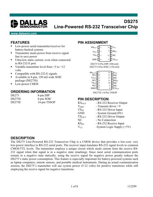

Create successful ePaper yourself
Turn your PDF publications into a flip-book with our unique Google optimized e-Paper software.
3 of 8<strong>DS275</strong>volts, and in many situations it can be tied directly to the +5 volt VCC supply. It is important to note thatVDRV must be greater than or equal to VCC at all times.The voltage range on VDRV permits the use of a 9-volt battery in order to provide a higher voltage levelwhen TXOUT is in a space state. When VCC is shut off to the <strong>DS275</strong> and VDRV is still powered (as mighthappen in a battery-backed condition), only a small leakage current (about 50-100 nA) will be drawn. IfTXOUT is loaded during such a condition, VDRV will draw current only if RXIN is not in a negative state.During normal operation (VCC=5 volts), VDRV will draw less than 2 uA when TXOUT is marking. Ofcourse, when TXOUT is spacing, VDRV will draw substantially more current⎯=about 3 mA, dependingupon its voltage and the impedance that TXOUT sees.The TXOUT output is slew rate-limited to less than 30 volts/us in accordance with <strong>RS</strong>-<strong>232</strong> specifications.In the event TXOUT should be inadvertently shorted to ground, internal current-limiting circuitry preventsdamage, even if continuously shorted.<strong>RS</strong>-<strong>232</strong> COMPATIBILITYThe intent of the <strong>DS275</strong> is not so much to meet all the requirements of the <strong>RS</strong>-<strong>232</strong> specification as tooffer a low-power solution that will work with most <strong>RS</strong>-<strong>232</strong> ports with a connector length of less than 10feet. As a prime example, the <strong>DS275</strong> will not meet the <strong>RS</strong>-<strong>232</strong> requirement that the signal levels be atleast ±5 volts minimum when terminated by a 3 kΩ=load and VDRV = +5 volts. Typically a voltage of 4volts will be present at TXOUT when spacing. However, since most <strong>RS</strong>-<strong>232</strong> receivers will correctlyinterpret any voltage over 2 volts as a space, there will be no problem transmitting data.APPLICATIONS INFORMATIONThe <strong>DS275</strong> is designed as a low-cost, <strong>RS</strong>-<strong>232</strong>-E interface expressly tailored for the unique requirementsof battery-operated handheld products. As shown in the electrical specifications, the <strong>DS275</strong> drawsexceptionally low operating and static current. During normal operation when data from the handheldsystem is sent from the TXOUT output, the <strong>DS275</strong> only draws significant VDRV current when TXOUTtransitions positively (spacing). This current flows primarily into the <strong>RS</strong>-<strong>232</strong> receiver’s 3-7 kΩ=load at theother end of the attaching cable. When TXOUT is marking (a negative data signal), the VDRV current fallsdramatically since the negative voltage is provided by the transmit signal from the other end of the cable.This represents a large reduction in overall operating current, since typical <strong>RS</strong>-<strong>232</strong> interface chips usecharge-pump circuits to establish both positive and negative levels at the transmit driver output.To obtain the lowest power consumption from the <strong>DS275</strong>, observe the following guidelines. First, tominimize VDRV current when connected to an <strong>RS</strong>-<strong>232</strong> port, always maintain TXIN at a logic 1 when data isnot being transmitted (idle state). This will force TXOUT into the marking state, minimizing VDRV current.Second, VDRV current will drop to less than 100 nA when VCC is grounded. Therefore, if VDRV is tieddirectly to the system battery, the logic +5 volts can be turned off to achieve the lowest possible powerstate.FULL-DUPLEX OPERATIONThe <strong>DS275</strong> is intended primarily for half-duplex operation; that is, RXIN should remain idle in themarking state when transmitting data out TXOUT and visa versa. However, the part can be operated fullduplexwith most <strong>RS</strong>-<strong>232</strong>-E serial ports since signals swinging between 0 and +5V will usually becorrectly interpreted by an <strong>RS</strong>-<strong>232</strong>-E receiver device. The 5-volt swing occurs when TXOUT attempts toswing negative while RXIN is at a positive voltage, which turns on an internal weak pulldown to groundfor the TXOUT driver’s negative reference. So, transmit mark signals at TXOUT may have voltage jumpsfrom some negative value (corresponding to RXIN marking) to approximately ground. One possible
<strong>DS275</strong>problem that may occur in this case is if the receiver at the other end requires a negative voltage forrecognizing a mark. In this situation, the full-duplex circuit shown in Figure 3 can be used asanalternative. The 22 µF capacitor forms a negative-charge reservoir; consequently, when the TXD line isspacing (positive), TXOUT still has a negative source available for a time period determined by thecapacitor and the load resistance at the other end (3-7 kΩ). This circuit was tested from 150-19,200 bpswith error-free operation using a SN75154 Quad <strong>Line</strong> Receiver as the receiver for the TXOUT signal. Notethat the SN75154 can have a marking input threshold below ground; hence there is the need for TXOUT toswing both positive and negative in full-duplex operation with this device.HANDHELD <strong>RS</strong>-<strong>232</strong>-C APPLICATION USING A STEREO MINI-JACK Figure 2FULL-DUPLEX CIRCUIT USING NEGATIVE-CHARGE STORAGE Figure 3NOTE:The capacitor stores negative charge whenever the TXD signal from the PC serial port is in a markingdata state (a negative voltage that is typically -10 volts). The top <strong>DS275</strong>’s TXOUT uses this negativecharge reservoir when it is in a marking state. The capacitor will discharge to 0 volts when the TXD lineis spacing (and TXOUT is still marking) at a time constant determined by its value and the value of the loadresistance reflected back to TXOUT. However, when TXD is marking the capacitor will quickly chargeback to -10 volts. Note that TXD remains in a marking state when idle, which improves the performanceof this circuit.ABSOLUTE MAXIMUM RATINGS*VCCVDRV-0.3 to +7.0 volts-0.3 to +13.0 volts4 of 8
±15 volts-0.3 to VCC + 0.3 volts±15 voltsRXOUT-0.3 to VCC + 0.3 voltsStorage Temperature-55°C to +125°COperating Temperature 0°C to 70°CRXINTXINTXOUT<strong>DS275</strong>* This is a stress rating only and functional operation of the device at these or any other conditionsabove those indicated in the operation sections of this specification is not implied. Exposure toabsolute maximum rating conditions for extended periods of time may affect reliability.RECOMMENDED DC OPERATING CONDITIONSPARAMETER SYMBOL MIN TYP MAX UNITS NOTESLogic Supply V CC 4.5 5.0 5.5 V 1Transmit Driver Supply V DRV 4.5 5-12 13.0 V 1Logic 1 Input V IH 2.0 V CC +0.3 V 2Logic 0 Input V IL -0.3 +0.8 V<strong>RS</strong>-<strong>232</strong> Input Range (RX IN ) V <strong>RS</strong> -15 +15 VDynamic Supply CurrentTX IN = V CCTX IN = GNDStatic Supply CurrentTX IN = V CCTX IN = GNDDriver LeakageCurrent (V CC =0V)I DRV1400I CC140I DRV13.8I CC1 40I DRV21.5I CC210.0I DRV23.8I CC2 10.08001005.010010.015.05.020.0µAµAµAµAµAµAmAµAI DRV3 0.05 1.0 µA 5345 of 8
DC ELECTRICAL CHARACTERISTICS (0°C to 70°C; VCC = VDRV = 5V ±=10%)PARAMETER SYMBOL MIN TYP MAX UNITS NOTESTX OUT Level High V OTXH 3.5 4.0 5.0 V 6TX OUT Level Low V OTXL -8.5 -9.0 V 7TX OUT Short Circuit Current I SC +60 +85 mATX OUT Output Slew Rate t SR 30 V/µsPropagation Delay t PD 5 µs 8RX IN Input Threshold Low V TL 0.8 1.2 1.6 VRX IN Input Threshold High V TH 1.6 2.0 2.4 VRX IN Threshold Hysteresis V HYS 0.5 0.8 V 9RX OUT Output Current @ 2.4V I OH -1.0 mARX OUT Output Current @ 0.4V I OL 3.2 mANOTES:1. VDRV must be greater than or equal to VCC.2. VCC = VDRV = 5V ±=10%.3. See test circuit in Figure 4.4. See test circuit in Figure 5.5. See test circuit in Figure 6.6. TXIN = VIL and TX OUT loaded by 3 kΩ=to ground.7. TXIN = VIH, RXIN = -10 volts and TXOUT loaded by 3 kΩ=to ground.8. TXIN to TXOUT - see Figure 7.9. VHYS = VTH - VTL.<strong>DS275</strong>6 of 8
DYNAMIC OPERATING CURRENTTEST CIRCUIT Figure 4<strong>DS275</strong>DRIVER LEAKAGE TEST CIRCUITFigure 6STATIC OPERATING CURRENTTEST CIRCUIT Figure 57 of 8
PROPAGATION DELAY TEST CIRCUIT Figure 7<strong>DS275</strong><strong>DS275</strong>E 14-PIN TSSOPDIM14-PINMIN MAXA MM - 1.10A1 MM 0.05 -A2 MM 0.75 1.05B MM 0.18 0.30C MM 0.09 0.18D MM 4.90 5.10E MM 4.40 NOMe1 MM 0.65 BSCG MM 0.25 REFH MM 6.25 6.55L MM 0.50 0.70phi 0° 8°8 of 8