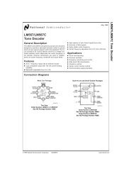
LM158/LM258/LM358/LM2904 Low Power Dual Operational ...
LM158/LM258/LM358/LM2904 Low Power Dual Operational ...
LM158/LM258/LM358/LM2904 Low Power Dual Operational ...
- No tags were found...

You also want an ePaper? Increase the reach of your titles
YUMPU automatically turns print PDFs into web optimized ePapers that Google loves.
<strong>LM158</strong>/<strong>LM258</strong>/<strong>LM358</strong>/<strong>LM2904</strong>Typical Performance Characteristics (Continued)Supply CurrentVoltage GainDS007787-36DS007787-37Open Loop FrequencyResponseCommon-ModeRejection RatioDS007787-38DS007787-39Voltage Follower PulseResponseVoltage Follower PulseResponse (Small Signal)DS007787-40DS007787-41www.national.com 6
Typical Performance Characteristics (Continued)Large Signal FrequencyResponseOutput CharacteristicsCurrent Sourcing<strong>LM158</strong>/<strong>LM258</strong>/<strong>LM358</strong>/<strong>LM2904</strong>DS007787-42DS007787-43Output CharacteristicsCurrent SinkingCurrent LimitingDS007787-44DS007787-45Input Current (LM2902 only)Voltage Gain (LM2902 only)Application HintsDS007787-46The <strong>LM158</strong> series are op amps which operate with only asingle power supply voltage, have true-differential inputs,and remain in the linear mode with an input common-modevoltage of 0 V DC . These amplifiers operate over a wide rangeof power supply voltage with little change in performancecharacteristics. At 25˚C amplifier operation is possible downto a minimum supply voltage of 2.3 V DC .DS007787-47Precautions should be taken to insure that the power supplyfor the integrated circuit never becomes reversed in polarityor that the unit is not inadvertently installed backwards in atest socket as an unlimited current surge through the resultingforward diode within the IC could cause fusing of the internalconductors and result in a destroyed unit.Large differential input voltages can be easily accomodatedand, as input differential voltage protection diodes are notneeded, no large input currents result from large differentialinput voltages. The differential input voltage may be larger7www.national.com
<strong>LM158</strong>/<strong>LM258</strong>/<strong>LM358</strong>/<strong>LM2904</strong>Application Hints (Continued)than V + without damaging the device. Protection should beprovided to prevent the input voltages from going negativemore than −0.3 V DC (at 25˚C). An input clamp diode with aresistor to the IC input terminal can be used.To reduce the power supply current drain, the amplifiershave a class A output stage for small signal levels which convertsto class B in a large signal mode. This allows the amplifiersto both source and sink large output currents. Thereforeboth NPN and PNP external current boost transistorscan be used to extend the power capability of the basic amplifiers.The output voltage needs to raise approximately 1diode drop above ground to bias the on-chip vertical PNPtransistor for output current sinking applications.For ac applications, where the load is capacitively coupled tothe output of the amplifier, a resistor should be used, fromthe output of the amplifier to ground to increase the class Abias current and prevent crossover distortion. Where theload is directly coupled, as in dc applications, there is nocrossover distortion.Capacitive loads which are applied directly to the output ofthe amplifier reduce the loop stability margin. Values of 50pF can be accomodated using the worst-case non-invertingunity gain connection. Large closed loop gains or resistiveisolation should be used if larger load capacitance must bedriven by the amplifier.The bias network of the <strong>LM158</strong> establishes a drain currentwhich is independent of the magnitude of the power supplyvoltage over the range of 3 V DC to 30 V DC .Output short circuits either to ground or to the positive powersupply should be of short time duration. Units can be destroyed,not as a result of the short circuit current causingmetal fusing, but rather due to the large increase in IC chipdissipation which will cause eventual failure due to excessivefunction temperatures. Putting direct short-circuits onmore than one amplifier at a time will increase the total ICpower dissipation to destructive levels, if not properly protectedwith external dissipation limiting resistors in serieswith the output leads of the amplifiers. The larger value ofoutput source current which is available at 25˚C provides alarger output current capability at elevated temperatures(see typical performance characteristics) than a standard ICop amp.The circuits presented in the section on typical applicationsemphasize operation on only a single power supply voltage.If complementary power supplies are available, all of thestandard op amp circuits can be used. In general, introducinga pseudo-ground (a bias voltage reference of V + /2) willallow operation above and below this value in single powersupply systems. Many application circuits are shown whichtake advantage of the wide input common-mode voltagerange which includes ground. In most cases, input biasing isnot required and input voltages which range to ground caneasily be accommodated.Connection Diagrams8-Bump micro SMDTop View(Bump Side Down)micro SMD Marking OrientationBumps are numbered counter-clockwise.Top ViewDS007787-56Metal Can PackageTop ViewDS007787-1DS007787-55www.national.com 8
Connection Diagrams (Continued)DIP/SO Package<strong>LM158</strong>/<strong>LM258</strong>/<strong>LM358</strong>/<strong>LM2904</strong>Top ViewOrdering InformationDS007787-2SO-8Package8-Pin MoldedDIP8-Pin CeramicDIPTO-5, 8-PinMetal Can8-Bump microSMDTemperature Range−55˚C to 125˚C −25˚C to 85˚C 0˚C to 70˚C −40˚C to 85˚C<strong>LM358</strong>AM <strong>LM2904</strong>M<strong>LM358</strong>AMX<strong>LM358</strong>M<strong>LM358</strong>MX<strong>LM158</strong>AJ/883(Note 11)<strong>LM158</strong>J/883(Note 11)<strong>LM158</strong>J<strong>LM158</strong>AJLQML(Note 12)<strong>LM158</strong>AJQMLV(Note 12)<strong>LM158</strong>AH/883(Note 11)<strong>LM158</strong>H/883(Note 11)<strong>LM158</strong>AH<strong>LM158</strong>H<strong>LM158</strong>AHLQML(Note 12)<strong>LM158</strong>AHLQMLV(Note12)<strong>LM258</strong>H<strong>LM358</strong>AN<strong>LM358</strong>N<strong>LM358</strong>H<strong>LM358</strong>BP<strong>LM358</strong>BPX<strong>LM2904</strong>NNSC DrawingM08AN08EJ08AH08CBPA08AAANote 11: <strong>LM158</strong> is available per SMD #5962-8771001<strong>LM158</strong>A is available per SMD #5962-8771002Note 12: See STD Mil DWG 5962L87710 for Radiation Tolerant Devices9www.national.com
<strong>LM158</strong>/<strong>LM258</strong>/<strong>LM358</strong>/<strong>LM2904</strong>Typical Single-Supply Applications (V + = 5.0 V DC )Non-Inverting DC Gain (0V Output)DS007787-6DS007787-7*R not needed due to temperature independent I INDC Summing Amplifier(V IN’S ≥ 0V DC and V O ≥ 0V DC )<strong>Power</strong> AmplifierV O =0V DC for V IN =0V DCDS007787-8A V =10Where: V O =V 1 +V 2 +V 3 +V 4(V 1 +V 2 )≥(V 3 +V 4 ) to keep V O > 0V DCDS007787-9www.national.com 10
Typical Single-Supply Applications (V + = 5.0 V DC ) (Continued)“BI-QUAD” RC Active Bandpass Filter<strong>LM158</strong>/<strong>LM258</strong>/<strong>LM358</strong>/<strong>LM2904</strong>f o = 1 kHzQ=50A v = 100 (40 dB)DS007787-10Fixed Current SourcesLamp DriverDS007787-12DS007787-1111www.national.com
<strong>LM158</strong>/<strong>LM258</strong>/<strong>LM358</strong>/<strong>LM2904</strong>Typical Single-Supply Applications (V + = 5.0 V DC ) (Continued)LED DriverCurrent MonitorDS007787-13DS007787-14*(Increase R1 for I L small)V L ≤ V + −2VDriving TTLVoltage FollowerDS007787-15DS007787-17V O =V INPulse GeneratorDS007787-16www.national.com 12
Typical Single-Supply Applications (V + = 5.0 V DC ) (Continued)Squarewave OscillatorPulse Generator<strong>LM158</strong>/<strong>LM258</strong>/<strong>LM358</strong>/<strong>LM2904</strong>DS007787-18DS007787-19<strong>Low</strong> Drift Peak DetectorDS007787-20HIGH Z INLOW Z OUT13www.national.com
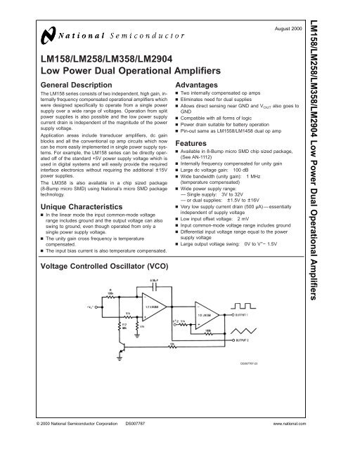
<strong>LM158</strong>/<strong>LM258</strong>/<strong>LM358</strong>/<strong>LM2904</strong>Typical Single-Supply Applications (V + = 5.0 V DC ) (Continued)High Compliance Current SinkComparator with HysteresisDS007787-22DS007787-21I O = 1 amp/volt V IN(Increase R E for I O small)Voltage Controlled Oscillator (VCO)*WIDE CONTROL VOLTAGE RANGE: 0 V DC ≤ V C ≤ 2(V + −1.5V DC )DS007787-23www.national.com 14
Typical Single-Supply Applications (V + = 5.0 V DC ) (Continued)AC Coupled Inverting Amplifier<strong>LM158</strong>/<strong>LM258</strong>/<strong>LM358</strong>/<strong>LM2904</strong>DS007787-24Ground Referencing a Differential Input SignalDS007787-2515www.national.com
<strong>LM158</strong>/<strong>LM258</strong>/<strong>LM358</strong>/<strong>LM2904</strong>Typical Single-Supply Applications (V + = 5.0 V DC ) (Continued)AC Coupled Non-Inverting AmplifierDS007787-26A v = 11 (As Shown)DC Coupled <strong>Low</strong>-Pass RC Active Filterf o = 1 kHzQ=1A V =2DS007787-27www.national.com 16
Typical Single-Supply Applications (V + = 5.0 V DC ) (Continued)Bandpass Active Filter<strong>LM158</strong>/<strong>LM258</strong>/<strong>LM358</strong>/<strong>LM2904</strong>f o = 1 kHzQ=25DS007787-28High Input Z, DC Differential AmplifierDS007787-2917www.national.com
<strong>LM158</strong>/<strong>LM258</strong>/<strong>LM358</strong>/<strong>LM2904</strong>Typical Single-Supply Applications (V + = 5.0 V DC ) (Continued)Photo Voltaic-Cell AmplifierBridge Current AmplifierDS007787-30DS007787-33High Input Z Adjustable-GainDC Instrumentation AmplifierDS007787-31www.national.com 18
Physical Dimensions inches (millimeters) unless otherwise noted (Continued)<strong>LM158</strong>/<strong>LM258</strong>/<strong>LM358</strong>/<strong>LM2904</strong>S.O. Package (M)Order Number <strong>LM358</strong>M, <strong>LM358</strong>AM or <strong>LM2904</strong>MNS Package Number M08A21www.national.com
<strong>LM158</strong>/<strong>LM258</strong>/<strong>LM358</strong>/<strong>LM2904</strong>Physical Dimensions inches (millimeters) unless otherwise noted (Continued)Molded Dip Package (N)Order Number <strong>LM358</strong>AN, <strong>LM358</strong>N or <strong>LM2904</strong>NNS Package Number N08EOrder Number <strong>LM158</strong>AWG/883NS Package Number W14Bwww.national.com 22
Physical Dimensions inches (millimeters) unless otherwise noted (Continued)NOTES: UNLESS OTHERWISE SPECIFIED1. EPOXY COATING2. 63Sn/37Pb EUTECTIC BUMP3. RECOMMEND NON-SOLDER MASK DEFINED LANDING PAD.4. PIN 1 IS ESTABLISHED BY LOWER LEFT CORNER WITH RESPECT TO TEXT ORIENTATION REMAINING PINS ARENUMBERED COUNTERCLOCKWISE.5. XXX IN DRAWING NUMBER REPRESENTS PACKAGE SIZE VARIATION WHERE X 1 IS PACKAGE WIDTH, X 2 IS PACK-AGE LENGTH AND X 3 IS PACKAGE HEIGHT.6. REFERENCE JEDEC REGISTRATION MO-211, VARIATION BC.8-Bump micro SMDNS Package Number BPA08AAAX 1 = 1.285 X 2 = 1.285 X 3 = 0.700LIFE SUPPORT POLICYNATIONAL’S PRODUCTS ARE NOT AUTHORIZED FOR USE AS CRITICAL COMPONENTS IN LIFE SUPPORTDEVICES OR SYSTEMS WITHOUT THE EXPRESS WRITTEN APPROVAL OF THE PRESIDENT AND GENERALCOUNSEL OF NATIONAL SEMICONDUCTOR CORPORATION. As used herein:1. Life support devices or systems are devices orsystems which, (a) are intended for surgical implantinto the body, or (b) support or sustain life, andwhose failure to perform when properly used inaccordance with instructions for use provided in thelabeling, can be reasonably expected to result in asignificant injury to the user.2. A critical component is any component of a lifesupport device or system whose failure to performcan be reasonably expected to cause the failure ofthe life support device or system, or to affect itssafety or effectiveness.<strong>LM158</strong>/<strong>LM258</strong>/<strong>LM358</strong>/<strong>LM2904</strong> <strong>Low</strong> <strong>Power</strong> <strong>Dual</strong> <strong>Operational</strong> AmplifiersNational SemiconductorCorporationAmericasTel: 1-800-272-9959Fax: 1-800-737-7018Email: support@nsc.comwww.national.comNational SemiconductorEuropeFax: +49 (0) 180-530 85 86Email: europe.support@nsc.comDeutsch Tel: +49 (0) 69 9508 6208English Tel: +44 (0) 870 24 0 2171Français Tel: +33 (0) 1 41 91 8790National SemiconductorAsia Pacific CustomerResponse GroupTel: 65-2544466Fax: 65-2504466Email: ap.support@nsc.comNational SemiconductorJapan Ltd.Tel: 81-3-5639-7560Fax: 81-3-5639-7507National does not assume any responsibility for use of any circuitry described, no circuit patent licenses are implied and National reserves the right at any time without notice to change said circuitry and specifications.