LM158/LM258/LM358/LM2904 Low Power Dual Operational ...
LM158/LM258/LM358/LM2904 Low Power Dual Operational ...
LM158/LM258/LM358/LM2904 Low Power Dual Operational ...
- No tags were found...

Create successful ePaper yourself
Turn your PDF publications into a flip-book with our unique Google optimized e-Paper software.
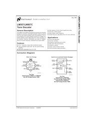
<strong>LM158</strong>/<strong>LM258</strong>/<strong>LM358</strong>/<strong>LM2904</strong>Application Hints (Continued)than V + without damaging the device. Protection should beprovided to prevent the input voltages from going negativemore than −0.3 V DC (at 25˚C). An input clamp diode with aresistor to the IC input terminal can be used.To reduce the power supply current drain, the amplifiershave a class A output stage for small signal levels which convertsto class B in a large signal mode. This allows the amplifiersto both source and sink large output currents. Thereforeboth NPN and PNP external current boost transistorscan be used to extend the power capability of the basic amplifiers.The output voltage needs to raise approximately 1diode drop above ground to bias the on-chip vertical PNPtransistor for output current sinking applications.For ac applications, where the load is capacitively coupled tothe output of the amplifier, a resistor should be used, fromthe output of the amplifier to ground to increase the class Abias current and prevent crossover distortion. Where theload is directly coupled, as in dc applications, there is nocrossover distortion.Capacitive loads which are applied directly to the output ofthe amplifier reduce the loop stability margin. Values of 50pF can be accomodated using the worst-case non-invertingunity gain connection. Large closed loop gains or resistiveisolation should be used if larger load capacitance must bedriven by the amplifier.The bias network of the <strong>LM158</strong> establishes a drain currentwhich is independent of the magnitude of the power supplyvoltage over the range of 3 V DC to 30 V DC .Output short circuits either to ground or to the positive powersupply should be of short time duration. Units can be destroyed,not as a result of the short circuit current causingmetal fusing, but rather due to the large increase in IC chipdissipation which will cause eventual failure due to excessivefunction temperatures. Putting direct short-circuits onmore than one amplifier at a time will increase the total ICpower dissipation to destructive levels, if not properly protectedwith external dissipation limiting resistors in serieswith the output leads of the amplifiers. The larger value ofoutput source current which is available at 25˚C provides alarger output current capability at elevated temperatures(see typical performance characteristics) than a standard ICop amp.The circuits presented in the section on typical applicationsemphasize operation on only a single power supply voltage.If complementary power supplies are available, all of thestandard op amp circuits can be used. In general, introducinga pseudo-ground (a bias voltage reference of V + /2) willallow operation above and below this value in single powersupply systems. Many application circuits are shown whichtake advantage of the wide input common-mode voltagerange which includes ground. In most cases, input biasing isnot required and input voltages which range to ground caneasily be accommodated.Connection Diagrams8-Bump micro SMDTop View(Bump Side Down)micro SMD Marking OrientationBumps are numbered counter-clockwise.Top ViewDS007787-56Metal Can PackageTop ViewDS007787-1DS007787-55www.national.com 8