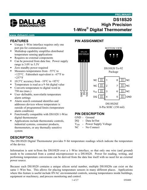
High Precision 1-Wire Digital Thermometer - Robot Store (HK)
High Precision 1-Wire Digital Thermometer - Robot Store (HK)
High Precision 1-Wire Digital Thermometer - Robot Store (HK)

You also want an ePaper? Increase the reach of your titles
YUMPU automatically turns print PDFs into web optimized ePapers that Google loves.
DS18S20 BLOCK DIAGRAM Figure 1DS18S20DQMEMORY ANDCONTROL LOGICINTERNAL V DD64-BIT ROMAND1-WIRE PORTSCRATCHPADTEMPERATURESENSORHIGH TEMPERATURETRIGGER, THV DDPOWERSUPPLYSENSE8-BIT CRCGENERATORLOW TEMPERATURETRIGGER, THPARASITE POWERThe block diagram (Figure 1) shows the parasite-powered circuitry. This circuitry “steals” powerwhenever the DQ or V DD pins are high. DQ will provide sufficient power as long as the specified timingand voltage requirements are met (see the section titled “1–<strong>Wire</strong> Bus System”). The advantages ofparasite power are twofold: 1) by parasiting off this pin, no local power source is needed for remotesensing of temperature, and 2) the ROM may be read in absence of normal power.In order for the DS18S20 to be able to perform accurate temperature conversions, sufficient power mustbe provided over the DQ line when a temperature conversion is taking place. Since the operating currentof the DS18S20 is up to 1.5 mA, the DQ line will not have sufficient drive due to the 5k pullup resistor.This problem is particularly acute if several DS18S20s are on the same DQ and attempting to convertsimultaneously.There are two ways to assure that the DS18S20 has sufficient supply current during its active conversioncycle. The first is to provide a strong pullup on the DQ line whenever temperature conversions or copiesto the E 2 memory are taking place. This may be accomplished by using a MOSFET to pull the DQ linedirectly to the power supply as shown in Figure 2. The DQ line must be switched over to the strongpull-up within 10 µs maximum after issuing any protocol that involves copying to the E 2 memory orinitiates temperature conversions. When using the parasite power mode, the V DD pin must be tied toground.Another method of supplying current to the DS18S20 is through the use of an external power supply tiedto the V DD pin, as shown in Figure 3. The advantage to this is that the strong pullup is not required on theDQ line, and the bus master need not be tied up holding that line high during temperature conversions.This allows other data traffic on the 1–<strong>Wire</strong> bus during the conversion time. In addition, any number ofDS18S20s may be placed on the 1–<strong>Wire</strong> bus, and if they all use external power, they may allsimultaneously perform temperature conversions by issuing the Skip ROM command and then issuing theConvert T command. Note that as long as the external power supply is active, the GND pin may not befloating.The use of parasite power is not recommended above 100°C, since it may not be able to sustaincommunications given the higher leakage currents the DS18S20 exhibits at these temperatures. Forapplications in which such temperatures are likely, it is strongly recommended that V DD be applied to theDS18S20.3 of 27
DS18S20For situations where the bus master does not know whether the DS18S20s on the bus are parasitepowered or supplied with external V DD , a provision is made in the DS18S20 to signal the power supplyscheme used. The bus master can determine if any DS18S20s are on the bus which require the strongpullup by sending a Skip ROM protocol, then issuing the read power supply command. After thiscommand is issued, the master then issues read time slots. The DS18S20 will send back “0” on the1-<strong>Wire</strong> bus if it is parasite powered; it will send back a “1” if it is powered from the V DD pin. If themaster receives a “0,” it knows that it must supply the strong pullup on the DQ line during temperatureconversions. See “Memory Command Functions” section for more detail on this command protocol.STRONG PULL-UP FOR SUPPLYING DS18S20 DURING TEMPERATURECONVERSION Figure 2+3V - +5VDS18S20+3V - +5VµP4.7kI/OGNDV DDUSING V DD TO SUPPLY TEMPERATURE CONVERSION CURRENT Figure 3DS18S20TO OTHER1-WIRE DEVICES+3V - +5VµP4.7kI/OGNDV DDEXTERNAL +3V - +5VSUPPLY4 of 27
DS18S20OPERATION – MEASURING TEMPERATUREThe core functionality of the DS18S20 is its direct-to-digital temperature sensor. The direct readout oftemperature data is 9 bits wide, equating to a resolution of 0.5°C; if higher resolution is desired, analgorithm is described later in this section to achieve that need. Following the issuance of the Convert T[44h] command, a temperature conversion is performed and the thermal data is stored in the scratchpadmemory in a 16-bit, sign-extended two’s complement format. The temperature information can beretrieved over the 1-<strong>Wire</strong> interface by issuing a Read Scratchpad [BEh] command once the conversionhas been performed. The data is transferred over the 1-<strong>Wire</strong> bus, LSB first. The MSB of the temperatureregister contains the “sign” (S) bit, denoting whether the temperature is positive or negative.Table 2 describes the exact relationship of output data to measured. For Fahrenheit usage, a lookup tableor conversion routine must be used.Temperature/Data Relationships Table 22 6 2 5 2 4 2 3 2 2 2 1 2 0 2 -1 LSBMSb (unit = °C) LSbS S S S S S S S MSBTEMPERATUREDIGITAL OUTPUT(Binary)5 of 27DIGITALOUTPUT(Hex)+85°C 0000 0101 0101 0000 0550h*+125°C 0000 0000 1111 1010 00FAh+25.0°C 0000 0000 0011 0010 0032h+0.5°C 0000 0000 0000 0001 0001h0°C 0000 0000 0000 0000 0000h-0.5°C 1111 1111 1111 1111 FFFFh-25.0°C 1111 1111 1100 1110 FFCEh-55°C 1111 1111 1001 0010 FF92h*The power on reset register value is +85°C<strong>High</strong>er resolutions may be obtained by the following procedure. First, read the temperature,COUNT_REMAIN, and COUNT_PER_C registers from the scratchpad. Truncate the 0.5°C bit (theLSB) from the temperature value. This value is TEMP_READ. The actual temperature may then becalculated by using the following:COUNT _ PER _ C − COUNT _ REMAINTEMPERATURE = TEMP _ READ − 0.25 +COUNT _ PER _ COPERATION – ALARM SIGNALINGAfter the DS18S20 has performed a temperature conversion, the temperature value is compared to thetrigger values stored in TH and TL. Since these registers are 8–bit only, the 0.5°C bit is ignored forcomparison. The most significant bit of TH or TL directly corresponds to the sign bit of the 16–bittemperature register. If the result of a temperature measurement is higher than TH or lower than TL, analarm flag inside the device is set. This flag is updated with every temperature measurement. As long as
DS18S20the alarm flag is set, the DS18S20 will respond to the alarm search command. This allows manyDS18S20s to be connected in parallel doing simultaneous temperature measurements. If somewhere thetemperature exceeds the limits, the alarming device(s) can be identified and read immediately withouthaving to read non–alarming devices.64-BIT LASERED ROMEach DS18S20 contains a unique ROM code that is 64–bits long. The first 8 bits are a 1–<strong>Wire</strong> familycode (DS18S20 code is 10h). The next 48 bits are a unique serial number. The last 8 bits are a CRC ofthe first 56 bits. (See Figure 4.) The 64–bit ROM and ROM Function Control section allow the DS18S20to operate as a 1–<strong>Wire</strong> device and follow the 1–<strong>Wire</strong> protocol detailed in the section “1–<strong>Wire</strong> BusSystem.” The functions required to control sections of the DS18S20 are not accessible until the ROMfunction protocol has been satisfied. This protocol is described in the ROM function protocol flowchart(Figure 5). The 1–<strong>Wire</strong> bus master must first provide one of five ROM function commands: 1) ReadROM, 2) Match ROM, 3) Search ROM, 4) Skip ROM, or 5) Alarm Search. After a ROM functionssequence has been successfully executed, the functions specific to the DS18S20 are accessible and thebus master may then provide one of the six memory and control function commands.CRC GENERATIONThe DS18S20 has an 8–bit CRC stored in the most significant byte of the 64–bit ROM. The bus mastercan compute a CRC value from the first 56–bits of the 64–bit ROM and compare it to the value storedwithin the DS18S20 to determine if the ROM data has been received error–free by the bus master. Theequivalent polynomial function of this CRC is:CRC = X 8 + X 5 + X 4 + 1The DS18S20 also generates an 8–bit CRC value using the same polynomial function shown above andprovides this value to the bus master to validate the transfer of data bytes. In each case where a CRC isused for data transfer validation, the bus master must calculate a CRC value using the polynomialfunction given above and compare the calculated value to either the 8–bit CRC value stored in the 64–bitROM portion of the DS18S20 (for ROM reads) or the 8–bit CRC value computed within the DS18S20(which is read as a ninth byte when the scratchpad is read). The comparison of CRC values and decisionto continue with an operation are determined entirely by the bus master. There is no circuitry inside theDS18S20 that prevents a command sequence from proceeding if the CRC stored in or calculated by theDS18S20 does not match the value generated by the bus master.The 1–<strong>Wire</strong> CRC can be generated using a polynomial generator consisting of a shift register and XORgates as shown in Figure 6. Additional information about the Dallas 1–<strong>Wire</strong> Cyclic Redundancy Check isavailable in Application Note 27 entitled “Understanding and Using Cyclic Redundancy Checks withDallas Semiconductor Touch Memory Products.”The shift register bits are initialized to “0”. Then starting with the least significant bit of the family code,one bit at a time is shifted in. After the eighth bit of the family code has been entered, then the serialnumber is entered. After the 48 th bit of the serial number has been entered, the shift register contains theCRC value. Shifting in the 8 bits of CRC should return the shift register to all “0s”.64-BIT LASERED ROM Figure 4MSB8-BIT CRC CODE 48-BIT SERIAL NUMBER 8-BIT FAMILY CODE (10h)LSB MSBLSB MSBLSB6 of 27
ROM FUNCTIONS FLOW CHART Figure 5DS18S20MASTER TXRESET PULSEDS18S20 TXPRESENCEPULSEMASTER TX ROMFUNCTION COMMAND33hREAD ROMCOMMANDEChN 55h NF0h N ALARM N CCh NMATCH ROMSEARCH ROMSEARCHSKIP ROMCOMMANDCOMMANDCOMMANDCOMMANDY Y Y Y YDS18S20 TXFAMILY CODE1 BYTEMASTER TXBIT 0ALARMCONDITION ?NYDS18S20 TX BIT 0DS18S20 TX BIT 0MASTER TX BIT 0DS18S20 TXSERIAL NUMBER6 BYTESBIT 0MATCH?NNBIT 0MATCH?YYDS18S20 TXCRC BYTEMASTER TXBIT 1DS18S20 TX BIT 1DS18S20 TX BIT 1MASTER TX BIT 1BIT 1MATCH?NNBIT 1MATCH?YYMASTER TXBIT 63DS18S20 TX BIT 63DS18S20 TX BIT 63MASTER TX BIT 63BIT 63MATCH?NNBIT 63MATCH?YYMASTER TX MEMORY OR CONTROLFUNCTION COMMAND7 of 27
1-WIRE CRC CODE Figure 6INPUTDS18S20XOR XOR XOR(MSB)(LSB)MEMORYThe DS18S20’s memory is organized as shown in Figure 7. The memory consists of a scratchpad RAMand a nonvolatile, electrically erasable (E 2 ) RAM, which stores the high and low temperature triggers, THand TL. The scratchpad helps insure data integrity when communicating over the 1–<strong>Wire</strong> bus. Data isfirst written to the scratchpad where it can be read back. After the data has been verified, a copyscratchpad command will transfer the data to the nonvolatile (E 2 ) RAM. This process insures dataintegrity when modifying the memory. The DS18S20 EEPROM is rated for a minimum of 50,000 writesand 10 years data retention at T = +55°C.The scratchpad is organized as 8 bytes of memory. The first 2-bytes contain the measured temperatureinformation. The third and fourth bytes are volatile copies of TH and TL and are refreshed with everypower–on reset. The next 2 bytes are not used; upon reading back, however, they will appear as all logic“1s”. The seventh and eighth bytes are count registers, which may be used in obtaining highertemperature resolution (see “Operation–measuring Temperature” section). There is a ninth byte whichmay be read with a Read Scratchpad command. This byte contains a cyclic redundancy check (CRC)byte which is the CRC over all of the 8 previous bytes. This CRC is implemented in the fashiondescribed in the section titled “CRC Generation."DS18S20 MEMORY MAP Figure 7SCRATCHPADTEMPERATURE LSBBYTE0E 2 RAMTEMPERATURE MSB1TH/USER BYTE 12TH/USER BYTE 1TL/USER BYTE 23TL/USER BYTE 2RESERVED4RESERVED5COUNT REMAIN6COUNT PER °C7CRC88 of 27
DS18S201-WIRE BUS SYSTEMThe 1–<strong>Wire</strong> bus is a system which has a single bus master and one or more slaves. The DS18S20behaves as a slave. The discussion of this bus system is broken down into three topics: hardwareconfiguration, transaction sequence, and 1–<strong>Wire</strong> signaling (signal types and timing).HARDWARE CONFIGURATIONThe 1–<strong>Wire</strong> bus has only a single line by definition; it is important that each device on the bus be able todrive it at the appropriate time. To facilitate this, each device attached to the 1–<strong>Wire</strong> bus must have opendrain or 3–state outputs. The 1–<strong>Wire</strong> port of the DS18S20 (DQ pin) is open drain with an internal circuitequivalent to that shown in Figure 8. A multidrop bus consists of a 1–<strong>Wire</strong> bus with multiple slavesattached. The 1–<strong>Wire</strong> bus requires a pullup resistor of approximately 5 kΩ.HARDWARE CONFIGURATION Figure 8BUS MASTER+3V - +5V4.7kDS18S20 1-WIRE PORTR XR X5 µATyp.T XT XR X = RECEIVET X = TRANSMIT100ΩMOSFETThe idle state for the 1–<strong>Wire</strong> bus is high. If for any reason a transaction needs to be suspended, the busMUST be left in the idle state if the transaction is to resume. Infinite recovery time can occur betweenbits so long as the 1–<strong>Wire</strong> bus is in the inactive (high) state during the recovery period. If this does notoccur and the bus is left low for more than 480 µs, all components on the bus will be reset.TRANSACTION SEQUENCEThe protocol for accessing the DS18S20 via the 1–<strong>Wire</strong> port is as follows:• Initialization• ROM Function Command• Memory Function Command• Transaction/Data9 of 27
DS18S20INITIALIZATIONAll transactions on the 1–<strong>Wire</strong> bus begin with an initialization sequence. The initialization sequenceconsists of a reset pulse transmitted by the bus master followed by presence pulse(s) transmitted by theslave(s).The presence pulse lets the bus master know that the DS18S20 is on the bus and is ready to operate. Formore details, see the “1–<strong>Wire</strong> Signaling” section.ROM FUNCTION COMMANDSOnce the bus master has detected a presence, it can issue one of the five ROM function commands. AllROM function commands are 8 bits long. A list of these commands follows (refer to flowchart inFigure 5):Read ROM [33h]This command allows the bus master to read the DS18S20’s 8–bit family code, unique 48–bit serialnumber, and 8–bit CRC. This command can only be used if there is a single DS18S20 on the bus. Ifmore than one slave is present on the bus, a data collision will occur when all slaves try to transmit at thesame time (open drain will produce a wired AND result).Match ROM [55h]The match ROM command, followed by a 64–bit ROM sequence, allows the bus master to address aspecific DS18S20 on a multidrop bus. Only the DS18S20 that exactly matches the 64–bit ROM sequencewill respond to the following memory function command. All slaves that do not match the 64–bit ROMsequence will wait for a reset pulse. This command can be used with a single or multiple devices on thebus.Skip ROM [CCh]This command can save time in a single drop bus system by allowing the bus master to access thememory functions without providing the 64–bit ROM code. If more than one slave is present on the busand a Read command is issued following the Skip ROM command, data collision will occur on the bus asmultiple slaves transmit simultaneously (open drain pulldowns will produce a wired AND result).Search ROM [F0h]When a system is initially brought up, the bus master might not know the number of devices on the1-<strong>Wire</strong> bus or their 64–bit ROM codes. The search ROM command allows the bus master to use aprocess of elimination to identify the 64–bit ROM codes of all slave devices on the bus.Alarm Search [ECh]The flowchart of this command is identical to the Search ROM command. However, the DS18S20 willrespond to this command only if an alarm condition has been encountered at the last temperaturemeasurement. An alarm condition is defined as a temperature higher than TH or lower than TL. Thealarm condition remains set as long as the DS18S20 is powered up, or until another temperaturemeasurement reveals a non–alarming value. For alarming, the trigger values stored in EEPROM aretaken into account. If an alarm condition exists and the TH or TL settings are changed, anothertemperature conversion should be done to validate any alarm conditions.10 of 27
11 of 27DS18S20Example of a ROM SearchThe ROM search process is the repetition of a simple three–step routine: read a bit, read the complementof the bit, then write the desired value of that bit. The bus master performs this simple, three–step routineon each bit of the ROM. After one complete pass, the bus master knows the contents of the ROM in onedevice. The remaining number of devices and their ROM codes may be identified by additional passes.The following example of the ROM search process assumes four different devices are connected to thesame 1–<strong>Wire</strong> bus. The ROM data of the four devices is as shown:ROM1 00110101...ROM2 10101010...ROM3 11110101...ROM4 00010001...The search process is as follows:1. The bus master begins the initialization sequence by issuing a reset pulse. The slave devices respondby issuing simultaneous presence pulses.2. The bus master will then issue the Search ROM command on the 1–<strong>Wire</strong> bus.3. The bus master reads a bit from the 1–<strong>Wire</strong> bus. Each device will respond by placing the value of thefirst bit of their respective ROM data onto the 1–<strong>Wire</strong> bus. ROM1 and ROM4 will place a 0 onto the1–<strong>Wire</strong> bus, i.e., pull it low. ROM2 and ROM3 will place a 1 onto the 1–<strong>Wire</strong> bus by allowing theline to stay high. The result is the logical AND of all devices on the line, therefore the bus mastersees a 0. The bus master reads another bit. Since the Search ROM data command is being executed,all of the devices on the 1–<strong>Wire</strong> bus respond to this second read by placing the complement of thefirst bit of their respective ROM data onto the 1–<strong>Wire</strong> bus. ROM1 and ROM4 will place a 1 onto the1–<strong>Wire</strong>, allowing the line to stay high. ROM2 and ROM3 will place a 0 onto the 1–<strong>Wire</strong>, thus it willbe pulled low. The bus master again observes a 0 for the complement of the first ROM data bit. Thebus master has determined that there are some devices on the 1–<strong>Wire</strong> bus that have a 0 in the firstposition and others that have a 1.The data obtained from the two reads of the three–step routine have the following interpretations:00 There are still devices attached which have conflicting bits in this position.01 All devices still coupled have a 0–bit in this bit position.10 All devices still coupled have a 1–bit in this bit position.11 There are no devices attached to the 1–<strong>Wire</strong> bus.4. The bus master writes a 0. This deselects ROM2 and ROM3 for the remainder of this search pass,leaving only ROM1 and ROM4 connected to the 1–<strong>Wire</strong> bus.5. The bus master performs two more reads and receives a 0–bit followed by a 1–bit. This indicates thatall devices still coupled to the bus have 0s as their second ROM data bit.6. The bus master then writes a 0 to keep both ROM1 and ROM4 coupled.7. The bus master executes two reads and receives two 0–bits. This indicates that both 1–bits and 0–bitsexist as the third bit of the ROM data of the attached devices.
DS18S208. The bus master writes a 0–bit. This deselects ROM1, leaving ROM4 as the only device stillconnected.9. The bus master reads the remainder of the ROM bits for ROM4 and continues to access the part ifdesired. This completes the first pass and uniquely identifies one part on the 1–<strong>Wire</strong> bus.10. The bus master starts a new ROM search sequence by repeating steps 1 through 7.11. The bus master writes a 1–bit. This decouples ROM4, leaving only ROM1 still coupled.12. The bus master reads the remainder of the ROM bits for ROM1 and communicates to the underlyinglogic if desired. This completes the second ROM search pass, in which another of the ROMs wasfound.13. The bus master starts a new ROM search by repeating steps 1 through 3.14. The bus master writes a 1–bit. This deselects ROM1 and ROM4 for the remainder of this search pass,leaving only ROM2 and ROM3 coupled to the system.15. The bus master executes two Read time slots and receives two 0s.16. The bus master writes a 0–bit. This decouples ROM3, leaving only ROM2.17. The bus master reads the remainder of the ROM bits for ROM2 and communicates to the underlyinglogic if desired. This completes the third ROM search pass, in which another of the ROMs wasfound.18. The bus master starts a new ROM search by repeating steps 13 through 15.19. The bus master writes a 1–bit. This decouples ROM2, leaving only ROM3.20. The bus master reads the remainder of the ROM bits for ROM3 and communicates to the underlyinglogic if desired. This completes the fourth ROM search pass, in which another of the ROMs wasfound.NOTE:The bus master learns the unique ID number (ROM data pattern) of one 1–<strong>Wire</strong> device on each ROMSearch operation. The time required to derive the part’s unique ROM code is:960 µs + (8 + 3 x 64) 61 µs = 13.16 msThe bus master is therefore capable of identifying 75 different 1–<strong>Wire</strong> devices per second.I/O SIGNALINGThe DS18S20 requires strict protocols to insure data integrity. The protocol consists of several types ofsignaling on one line: reset pulse, presence pulse, write 0, write 1, read 0, and read 1. All of these signals,with the exception of the presence pulse, are initiated by the bus master.12 of 27
DS18S20The initialization sequence required to begin any communication with the DS18S20 is shown in Figure10. A reset pulse followed by a presence pulse indicates the DS18S20 is ready to send or receive datagiven the correct ROM command and memory function command.The bus master transmits (TX) a reset pulse (a low signal for a minimum of 480 ms). The bus masterthen releases the line and goes into a receive mode (RX). The 1–<strong>Wire</strong> bus is pulled to a high state via the5k pullup resistor. After detecting the rising edge on the DQ pin, the DS18S20 waits 15–60 µs and thentransmits the presence pulse (a low signal for 60–240 µs).MEMORY COMMAND FUNCTIONSThe following command protocols are summarized in Table 2, and by the flowchart of Figure 9.Write Scratchpad [4Eh]This command writes to the scratchpad of the DS18S20, starting at the TH register. The next 2 byteswritten will be saved in scratchpad memory at address locations 2 and 3. Writing may be terminated atany point by issuing a reset.Read Scratchpad [BEh]This command reads the contents of the scratchpad. Reading will commence at byte 0, and will continuethrough the scratchpad until the ninth (byte 8, CRC) byte is read. If not all locations are to be read, themaster may issue a reset to terminate reading at any time.Copy Scratchpad [48h]This command copies the scratchpad into the E 2 memory of the DS18S20, storing the temperature triggerbytes in nonvolatile memory. If the bus master issues read time slots following this command, theDS18S20 will output 0 on the bus as long as it is busy copying the scratchpad to E 2 ; it will return a 1when the copy process is complete. If parasite-powered, the bus master has to enable a strong pullup forat least 10 ms immediately after issuing this command. The DS18S20 EEPROM is rated for a minimumof 50,000 writes and 10 years data retention at T = +55°C.Convert T [44h]This command begins a temperature conversion. No further data is required. The temperatureconversion will be performed and then the DS18S20 will remain idle. If the bus master issues read timeslots following this command, the DS18S20 will output 0 on the bus as long as it is busy making atemperature conversion; it will return a 1 when the temperature conversion is complete. If parasitepowered,the bus master has to enable a strong pullup for a time period greater than t conv immediatelyafter issuing this command.Recall E2 [B8h]This command recalls the temperature trigger values stored in E 2 to the scratchpad. This recall operationhappens automatically upon power–up to the DS18S20 as well, so valid data is available in the scratchpadas soon as the device has power applied. With every read data time slot issued after this command hasbeen sent, the device will output its temperature converter busy flag: 0=busy, 1=ready.Read Power Supply [B4h]With every read data time slot issued after this command has been sent to the DS18S20, the device willsignal its power mode: 0=parasite power, 1=external power supply provided.13 of 27
MEMORY FUNCTIONS FLOW CHART Figure 9DS18S20MASTER TX MEMORY ORCONTROL COMMAND4EhWRITESCRATCHPAD?NBEhREADSCRATCHPAD?NYYDS18S20 SETS ADDRESSCOUNTER TO 2DS18S20 SETS ADDRESSCOUNTER TO 0MASTER TX DATA BYTETO SCRATCHPADMASTER RX DATAFROM SCRATCHPADMASTERTX RESET?YMASTERTX RESET?YNNADDRESS=3?YADDRESS=7?YNNDS18S20 INCREMENTSADDRESSDS18S20 TXDS18S20 INCREMENTSSERIAL NUMBERADDRESS6 BYTESNMASTERTX RESET?MASTER RX 8-BITCRC OF DATAYMASTERTX RESET?YNMASTER RX “1s”DS18S20 TXPRESENCE PULSE14 of 27
MEMORY FUNCTIONS FLOW CHART Figure 9 (cont’d)DS18S2048hCOPYSCRATCHPAD?N44hCONVERTTEMPERATURENYYNPARASITEPOWER?YNPARASITEPOWER?YMASTER ENABLESSTRONG PULLUP FOR10msMASTER ENABLESSTRONG PULL-UPMASTER DISABLESSTRONG PULLUPDS18S20 CONVERTSTEMPERATUREDS18S20 BEGINSCONVERSIONMASTER DISABLESSTRONG PULL-UPYYMASTER TXRESET?MASTER TXRESET?NNNNONVOLATILEMEMORYBUSY?YNDEVICE BUSYCONVERTINGTEMPERATURE?YMASTERRX “1”SMASTERRX “0”SMASTERRX “1”SMASTERRX “0”S15 of 27
MEMORY FUNCTIONS FLOW CHART Figure 9 (cont’d)DS18S20B8hRECALLE 2?YNB4hREADPOWERSUPPLY?YNDS18S20 RECALLSFROM E 2 PROMYYMASTER TXRESET?MASTER TXRESET?NNNDEVICEBUSY CONVERTINGTEMPERATURE?YNPARASITEPOWERED?YMASTERTX RESET?YNMASTERRX “1”SMASTERRX “0”SMASTERRX “1”SMASTERRX “0”S16 of 27
DS18S20INITIALIZATION PROCEDURE “RESET AND PRESENCE PULSES” Figure 10Master T X "reset pulse"480 µs minmum960 µs maximumDS18S20 TXwaits15-60 µsDS18S20 TX"presence Pulse"60-240 µsMaster R X480 µs minmum1-WIREBUSV CCGNDLINE TYPE LEGENDBus master active lowDS18S20 active lowBoth bus master andDS18S20 active lowResistor pull-upDS18S20 COMMAND SET Table 2INSTRUCTION DESCRIPTION PROTOCOL1-WIRE BUSAFTER ISSUINGPROTOCOL NOTESTEMPERATURE CONVERSION COMMANDSConvert T Initiates temperature44h MEMORY COMMANDSRead Scratchpad Reads bytes fromBEh scratchpad and readsCRC byte.Write Scratchpad Writes bytes intoscratchpad at addresses 24Eh and 3 (TH and TLtemperature triggers).Copy Scratchpad Copies scratchpad intononvolatile memory48h 2Recall E 2Read Power Supply(addresses 2 and 3 only).Recalls values stored innonvolatile memory intoscratchpad (temperaturetriggers).Signals the mode ofDS18S20 power supplyto the master.B8hB4h17 of 27
DS18S20NOTES:1. Temperature conversion takes up to 750 ms. After receiving the Convert T protocol, if the part doesnot receive power from the V DD pin, the DQ line for the DS18S20 must be held high for at least750 ms to provide power during the conversion process. As such, no other activity may take place onthe 1–<strong>Wire</strong> bus for at least this period after a Convert T command has been issued.2. After receiving the Copy Scratchpad protocol, if the part does not receive power from the V DD pin, theDQ line for the DS18S20 must be held high for at least 10 ms to provide power during the copyprocess. As such, no other activity may take place on the 1–<strong>Wire</strong> bus for at least this period after aCopy Scratchpad command has been issued.READ/WRITE TIME SLOTSDS18S20 data is read and written through the use of time slots to manipulate bits and a command word tospecify the transaction.Write Time SlotsA write time slot is initiated when the host pulls the data line from a high logic level to a low logic level.There are two types of write time slots: Write 1 time slots and Write 0 time slots. All write time slotsmust be a minimum of 60 µs in duration with a minimum of a 1-µs recovery time between individualwrite cycles.The DS18S20 samples the DQ line in a window of 15 µs to 60 µs after the DQ line falls. If the line ishigh, a Write 1 occurs. If the line is low, a Write 0 occurs (see Figure 11).For the host to generate a Write 1 time slot, the data line must be pulled to a logic low level and thenreleased, allowing the data line to pull up to a high level within 15 µs after the start of the write time slot.For the host to generate a Write 0 time slot, the data line must be pulled to a logic low level and remainlow for 60 µs.Read Time SlotsThe host generates read time slots when data is to be read from the DS18S20. A read time slot is initiatedwhen the host pulls the data line from a logic high level to logic low level. The data line must remain at alow logic level for a minimum of 1 µs; output data from the DS18S20 is valid for 15 µs after the fallingedge of the read time slot. The host therefore must stop driving the DQ pin low in order to read its state15 µs from the start of the read slot (see Figure 11). By the end of the read time slot, the DQ pin will pullback high via the external pullup resistor. All read time slots must be a minimum of 60 µs in durationwith a minimum of a 1-µs recovery time between individual read slots.Figure 12 shows that the sum of T INIT , T RC , and T SAMPLE must be less than 15 µs. Figure 13 shows thatsystem timing margin is maximized by keeping T INIT and T RC as small as possible and by locating themaster sample time towards the end of the 15-µs period.18 of 27
READ/WRITE TIMING DIAGRAM Figure 11DS18S20Master Write "0" Slot60 µs 1 µsDS18S20 SAMPLESMIN TYP MAX15 µs 15 µs 30 µs15 µs15 µs30 µsMaster Read "0" SlotMaster Read "1" Slot1 µs < t REC < ∞1-WIREBUSV CCGNDMaster Samples>1 µsMaster Samples15 µs 15 µs 30 µs15 µs30 µsLINE TYPE LEGENDBus master active lowDS18S20 active lowBoth bus master andDS18S20 active lowResistor pull-up19 of 27
DETAILED MASTER READ 1 TIMING Figure 12DS18S20V CC1-WIREBUSV IH OF MASTERGNDT INIT >1 µsT RCMASTER SAMPLES15 µsRECOMMENDED MASTER READ 1 TIMING Figure 13V CC1-WIREBUSV IH OF MASTERGNDT INIT =SMALLT RC =SMALL15 µsMASTER SAMPLESLINE TYPE LEGENDBus master active lowDS18S20 active lowBoth bus master andDS18S20 active lowResistor pull-up20 of 27
DS18S20Related Application NotesThe following Application Notes can be applied to the DS18S20. These notes can be obtained from theDallas Semiconductor “Application Note Book,” via our website at http://www.dalsemi.com/.Application Note 27: “Understanding and Using Cyclic Redundancy Checks with Dallas SemiconductorTouch Memory Product”Application Note 55: “Extending the Contact Range of Touch Memories”Application Note 74: “Reading and Writing Touch Memories via Serial Interfaces”Application Note 104: “Minimalist Temperature Control Demo”Application Note 105: “<strong>High</strong> Resolution Temperature Measurement with Dallas Direct–to–DirectTemperature Sensors”Application Note 106: “Complex MicroLANs”Application Note 108: “MicroLAN – In the Long Run”Sample 1–<strong>Wire</strong> subroutines that can be used in conjunction with AN74 can be downloaded from thewebsite or our Anonymous FTP Site.MEMORY FUNCTION EXAMPLE Table 3Example: Bus Master initiates temperature conversion, then reads temperature (parasite power assumed).MASTER MODE DATA (LSB FIRST) COMMENTSTX Reset Reset pulse (480-960 µs).RX Presence Presence pulse.TX 55h Issue “Match ROM” command.TX Issue address for DS18S20.TX 44h Issue “ Convert T” command.TX I/O line is held high for at least 750 ms by bus master toallow conversion to complete.TX Reset Reset pulse.RX Presence Presence pulse.TX 55h Issue “Match ROM” command.TX Issue address for DS18S20.TX BEh Issue “Read Scratchpad” command.RX Read entire scratchpad plus CRC; the master nowrecalculates the CRC of the eight data bytes receivedfrom the scratchpad, compares the CRC calculated andthe CRC read. If they match, the master continues; ifnot, this read operation is repeated.TX Reset Reset pulse.RX Presence Presence pulse, done.21 of 27
MEMORY FUNCTION EXAMPLE Table 4Example: Bus Master writes memory (parasite power and only one DS18S20 assumed).DS18S20MASTER MODE DATA (LSB FIRST) COMMENTSTX Reset Reset pulse.RX Presence Presence pulse.TX CCh Skip ROM command.TX 4Eh Write Scratchpad command.TX Writes 2 bytes to scratchpad (TH and TL).TX Reset Reset pulse.RX Presence Presence pulse.TX CCh Skip ROM command.TX BEh Read Scratchpad command.RX Read entire scratchpad plus CRC. The master nowrecalculates the CRC of the eight data bytes receivedfrom the scratchpad, compares the CRC and the twoother bytes read back from the scratchpad. If data match,the master continues; if not, repeat the sequence.TX Reset Reset pulse.RX Presence Presence pulse.TX CCh Skip ROM command.TX 48h Copy Scratchpad command; after issuing this command,the master must wait 10 ms for copy operation tocomplete.TX Reset Reset pulse.RX Presence Presence pulse, done.22 of 27
MEMORY FUNCTION EXAMPLE Table 5Example: Temperature conversion and interpolation (external power supply and only one DS18S20assumed.)DS18S20MASTER MODE DATA (LSB FIRST) COMMENTSTX Reset Reset pulse.TR Presence Presence pulse.TX CCh Skip ROM command.TX 44h Convert T command.RX Read busy flag eight times. The master continuesreading 1 byte (or bit) after another until the data is FFh(all bits 1).TX Reset Reset pulse.RX Presence Presence pulse.TX CCh Skip ROM command.TX BEh Read Scratchpad command.RX Read entire scratchpad plus CRC. The master nowrecalculates the CRC of the eight data bytes receivedfrom the scratchpad and compares both CRCs. If theCRCs match, the data is valid. The master saves thetemperature value and stores the contents of the countregister and count per °C register as COUNT_REMAINand COUNT_PER_C, respectively.TX Reset Reset pulse.RX Presence Presence pulse, done.- - CPU calculates temperature as described in the datasheet for higher resolution.23 of 27
ABSOLUTE MAXIMUM RATINGS*Voltage on Any Pin Relative to GroundOperating TemperatureStorage TemperatureSoldering Temperature–0.5V to +6.0V–55°C to +125°C–55°C to +125°CSee J-STD-020A specificationDS18S20* This is a stress rating only and functional operation of the device at these or any other conditions abovethose indicated in the operation sections of this specification is not implied. Exposure to absolutemaximum rating conditions for extended periods of time may affect reliability.RECOMMENDED DC OPERATING CONDITIONSPARAMETER SYMBOL CONDITION MIN TYP MAX UNITS NOTESSupply Voltage V DD Local Power 3.0 5.5 V 1Data Pin DQ -0.3 V DD V 1Logic 1 V IH 2.2 V DD +0.3 V 1,2Logic 0 V IL -0.3 +0.8 V 1,3,7DC ELECTRICAL CHARACTERISTICS(-55°C to +125°C; V DD =3.0V to 5.5V)PARAMETER SYMBOL CONDITION MIN TYP MAX UNITS NOTES<strong>Thermometer</strong> Error t ERR -10°C to +85°C ±½ °C-55°C to +125°C ±2Input Logic <strong>High</strong> V IH Local PowerParasite Power2.23.05.5 VV1,21,2Input Logic Low V IL -0.3 +0.8 V 1,3, 7Sink Current I L V I/O =0.4V -4.0 mA 1Standby Current I DDS 750 1000 nA 6,8Active Current I DD 1 1.5 mA 4DQ Input LoadCurrentI DQ 5 µA 5AC ELECTRICAL CHARACTERISTICS: NV MEMORY(-55°C to +125°C; V DD =3.0V to 5.5V)PARAMETER SYMBOL CONDITION MIN TYP MAX UNITS NOTESNV Write Cycle Time t WR 2 10 msEEPROM Writes N EEWR -55°C to +55°C 50k writesEEPROM Datat EEDR -55°C to +55°C 10 yearsRetention24 of 27
DS18S20AC ELECTRICAL CHARACTERISTICS:(-55°C to +125°C; V DD =3.0V to 5.5V)PARAMETER SYMBOL CONDITION MIN TYP MAX UNITS NOTESTemperature Conversion t CONV 200 750 msTimeTime Slot t SLOT 60 120 µsRecovery Time t REC 1 µsWrite 0 Low Time r LOW0 60 120 µsWrite 1 Low Time t LOW1 1 15 µsRead Data Valid t RDV 15 µsReset Time <strong>High</strong> t RSTH 480 µsReset Time Low t RSTL 480 µs 9Presence Detect <strong>High</strong> t PDHIGH 15 60 µsPresence Detect Low t PDLOW 60 240 µsCapacitance C IN/OUT 25 pFNOTES:1. All voltages are referenced to ground.2. Logic one voltages are specified at a source current of 1 mA.3. Logic zero voltages are specified at a sink current of 4 mA.4. Active current refers to either temperature conversion or writing to the E 2 memory. Writing to E 2memory consumes approximately 200 µA for up to 10 ms.5. Input load is to ground.6. Standby current specified up to 70°C. Standby current typically is 3 µA at 125°C.7. To always guarantee a presence pulse under low voltage parasite power conditions, V ILMAX may haveto be reduced to as much as 0.5V.8. To minimize I DDS , DQ should be GND ≤ DQ ≤ GND + 0.3V or V DD – 0.3V ≤ DQ ≤ V DD .9. Under parasite power, the max t RSTL before a power on reset occurs, is 960 ms.25 of 27
1—WIRE WRITE ONE TIME SLOTDS18S201—WIRE WRITE ZERO TIME SLOT1—WIRE READ ZERO TIME SLOT1—WIRE RESET PULSE1-WIRE PRESENCE DETEST26 of 27
TYPICAL PERFORMANCE CURVEDS18S20DS18S20 Typical Error Curve0.50.40.30.2+3σ Error0.100 10 20 30 40 50 60 70-0.1-0.2-0.3Mean Error-0.4-0.5Reference Temp (C)-3σ Error27 of 27