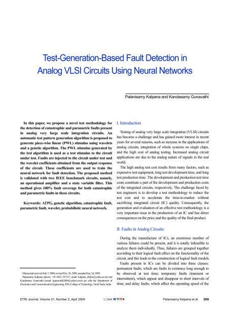
Test-Generation-Based Fault Detection in Analog ... - ETRI Journal
Test-Generation-Based Fault Detection in Analog ... - ETRI Journal
Test-Generation-Based Fault Detection in Analog ... - ETRI Journal

You also want an ePaper? Increase the reach of your titles
YUMPU automatically turns print PDFs into web optimized ePapers that Google loves.
<strong>Test</strong>-<strong>Generation</strong>-<strong>Based</strong> <strong>Fault</strong> <strong>Detection</strong> <strong>in</strong><strong>Analog</strong> VLSI Circuits Us<strong>in</strong>g Neural NetworksPalanisamy Kalpana and Kandasamy GunavathiIn this paper, we propose a novel test methodology forthe detection of catastrophic and parametric faults present<strong>in</strong> analog very large scale <strong>in</strong>tegration circuits. Anautomatic test pattern generation algorithm is proposed togenerate piece-wise l<strong>in</strong>ear (PWL) stimulus us<strong>in</strong>g waveletsand a genetic algorithm. The PWL stimulus generated bythe test algorithm is used as a test stimulus to the circuitunder test. <strong>Fault</strong>s are <strong>in</strong>jected to the circuit under test andthe wavelet coefficients obta<strong>in</strong>ed from the output responseof the circuit. These coefficients are used to tra<strong>in</strong> theneural network for fault detection. The proposed methodis validated with two IEEE benchmark circuits, namely,an operational amplifier and a state variable filter. Thismethod gives 100% fault coverage for both catastrophicand parametric faults <strong>in</strong> these circuits.Keywords: ATPG, genetic algorithm, catastrophic fault,parametric fault, wavelet, probabilistic neural network.I. Introduction<strong>Test</strong><strong>in</strong>g of analog very large scale <strong>in</strong>tegration (VLSI) circuitshas become a challenge and has ga<strong>in</strong>ed more <strong>in</strong>terest <strong>in</strong> recentyears for several reasons, such as <strong>in</strong>crease <strong>in</strong> the applications ofanalog circuits, <strong>in</strong>tegration of whole systems on s<strong>in</strong>gle chips,and the high cost of analog test<strong>in</strong>g. Increased analog circuitapplications are due to the analog nature of signals <strong>in</strong> the realworld.The high analog test cost results from many factors, such asexpensive test equipment, long test development time, and longtest production time. The development and production test timecosts constitute a part of the development and production costsof the <strong>in</strong>tegrated circuits, respectively. The challenge faced bytest eng<strong>in</strong>eers is to develop a test methodology to reduce thetest cost and to accelerate the time-to-market withoutsacrific<strong>in</strong>g <strong>in</strong>tegrated circuit (IC) quality. Consequently, thegeneration and evaluation of an effective test methodology is avery important issue <strong>in</strong> the production of an IC and has directconsequences on the price and the quality of the f<strong>in</strong>al product.II. <strong>Fault</strong>s <strong>in</strong> <strong>Analog</strong> CircuitsManuscript received July 7, 2008; revised Dec. 26, 2008; accepted Jan. 24, 2009.Palanisamy Kalpana (phone: +91 0422 257217, email: kalpana_shekar@yahoo.co.<strong>in</strong>) andKandasamy Gunavathi (email: kgunavathi2000@yahoo.com) are with the Department ofElectronics and Communication Eng<strong>in</strong>eer<strong>in</strong>g, PSG College of Technology, Tamil Nadu, India.Dur<strong>in</strong>g the manufacture of ICs, an enormous number ofvarious failures could be present, and it is totally <strong>in</strong>feasible toanalyze them <strong>in</strong>dividually. Thus, failures are grouped togetheraccord<strong>in</strong>g to their logical fault effect on the functionality of thecircuit, and this leads to the construction of logical fault models.<strong>Fault</strong>s present <strong>in</strong> ICs can be divided <strong>in</strong>to three classes:permanent faults, which are faults <strong>in</strong> existence long enough tobe observed at test time; temporary faults (transient or<strong>in</strong>termittent), which appear and disappear <strong>in</strong> short <strong>in</strong>tervals oftime; and delay faults, which affect the operat<strong>in</strong>g speed of the<strong>ETRI</strong> <strong>Journal</strong>, Volume 31, Number 2, April 2009 © 2009 Palanisamy Kalpana et al. 209
circuit.Permanent faults are further classified <strong>in</strong>to catastrophic faults(open and short) and parametric faults (due to disturbance <strong>in</strong>the process parameters). When a catastrophic fault occurs, thetopology of the circuit is changed. Due to parametric faults, theperformance parameters of each manufactured circuit deviatefrom the nom<strong>in</strong>al one and therefore correspond to a differentpo<strong>in</strong>t <strong>in</strong> each parameter space. If each parameter of the circuitis with<strong>in</strong> a fault free space, then the circuit is treated as faultfree; otherwise, it is considered a faulty circuit.In this paper, catastrophic and parametric faults are taken asfault models for analog circuits, which are designed withresistors, capacitors, MOSFETs, and bipolar junctiontransistors. The test<strong>in</strong>g issues related to these faults areaddressed <strong>in</strong> this study.III. <strong>Test</strong> Pattern <strong>Generation</strong>S<strong>in</strong>ce the cost of test<strong>in</strong>g a VLSI chip is a significant fractionof the manufactur<strong>in</strong>g cost, the time required to test a chipshould be m<strong>in</strong>imized, and there should be significant faultcoverage. The objective of the automatic test pattern generatoris to f<strong>in</strong>d an optimal set of test stimuli which detects allmodeled faults, that is, a set of test stimuli which when appliedto the circuit can dist<strong>in</strong>guish between the correct circuit and anycircuit with a modeled fault.The goal of the proposed approach is to compute a set of teststimuli that maximizes the fault coverage while m<strong>in</strong>imiz<strong>in</strong>gtest access. Therefore, the problem of test signal generation isan optimization problem <strong>in</strong> pr<strong>in</strong>ciple. <strong>Test</strong> vector generationus<strong>in</strong>g determ<strong>in</strong>istic techniques is highly complex and timeconsum<strong>in</strong>g because of the extremely large search spaces<strong>in</strong>volved. Therefore, artificial <strong>in</strong>telligence methods have ga<strong>in</strong>edmuch attention [1], [2].Genetic algorithms are search optimization algorithms basedon the mechanics of natural genetics that attempt to use similarmethods for selection and reproduction to solve variousoptimization problems. Genetic algorithms have proven to beeffective <strong>in</strong> VLSI applications, <strong>in</strong>clud<strong>in</strong>g circuit layout andpartition<strong>in</strong>g, cell placement, rout<strong>in</strong>g, and automatic testgeneration. The proposed method uses a genetic algorithm forthe generation of the test stimulus which detects bothcatastrophic and parametric faults present <strong>in</strong> the circuit undertest (CUT).In the literature, a genetic algorithm is used as a test patterngenerator [1], [2] to generate a piece-wise l<strong>in</strong>ear (PWL)stimulus. In [1] and [2], multiple node po<strong>in</strong>ts <strong>in</strong> the circuits areconsidered for detect<strong>in</strong>g faults <strong>in</strong> the CUT. However, <strong>in</strong>complex systems all nodes <strong>in</strong> the circuit may not be accessible.Therefore, <strong>in</strong> this work only the output node is considered formeasurements and the output response is analyzed us<strong>in</strong>gwavelets.1. PWL Signal <strong>Generation</strong>By excit<strong>in</strong>g the CUT with pulses and ramps whosefrequency spectrum stretches over a wide range of frequencies,all faults can be made visible <strong>in</strong> the measurement space. Thus,a transient PWL signal is generated for detection of bothcatastrophic and parametric faults present <strong>in</strong> the circuits. Togenerate the PWL test signal, a genetic algorithm is used. Each testvector is a transient stimulus.Figure 1 shows an example test vector. The amplitude limitfor each test vector is fixed based on the allowable range of<strong>in</strong>put signal for the circuit, and the frequency of the stimulus isfixed based on the allowable operat<strong>in</strong>g frequency of the circuits.For example, if a circuit has a supply voltage of 2.5 V, a ga<strong>in</strong> of2, and a 1 MHz bandwidth, then the amplitude range for thePWL stimulus is fixed from -1 to +1 and the frequency is fixedfrom 1 Hz to 1 MHz. The length of the PWL signal is fixedbased on the amplitude level and frequency of operation of theCUT. Initial random vectors (PWL test signals) are selectedsuch that all amplitude levels are covered.Amplitude1.51.00.50.0-0.5-1.0-1.52. Bounds for Parameters1 2 3 4 5 6 7 8TimeFig. 1. PWL test vector.For the given CUT, the bounds of the parameters are foundas follows.In general, a circuit is bounded by n specifications, S =[s 1 , s 2 ,∙∙∙, s n ]. For design<strong>in</strong>g the circuit, m parameters, P =[p 1 , p 2 ,∙∙∙, p m ] are used. Each specification is dependent on oneor more parameters. Under s<strong>in</strong>gle parametric (p i ) faultassumption, upper and lower bounds of the parameters arefixed for each specification. Given an acceptable range of s j(upper bound s j u , lower bound s j l ), the accepted tolerance rangeof p i (upper bound p iu, lower bound p i l ) can be found as shown<strong>in</strong> Fig. 2.The f<strong>in</strong>al upper and lower bounds of the accepted range forp i are found as follows:p u i = m<strong>in</strong> (p u i1 , p u i2 ,∙∙∙, p u <strong>in</strong> ), (1)p l i = max (p l i1 , p l i2 ,∙∙∙, p l <strong>in</strong> ). (2)210 Palanisamy Kalpana et al. <strong>ETRI</strong> <strong>Journal</strong>, Volume 31, Number 2, April 2009
Faills jlp ijFailp jlPassp iklPasss juNom<strong>in</strong>al valuep ijup ikuFailFailFig. 2. Bounds for parameters.After sett<strong>in</strong>g the bounds for parameters, the circuit issimulated under fault-free and faulty conditions.3. Feature Extraction Us<strong>in</strong>g WaveletsWavelet transform (WT) is capable of provid<strong>in</strong>g the time andfrequency resolution simultaneously and hence giv<strong>in</strong>g timefrequencyrepresentation of the signal. Deviation of anyparameter alters the specifications of the circuit. Thesespecifications may be represented as time doma<strong>in</strong> or frequencydoma<strong>in</strong> units. If both time and frequency doma<strong>in</strong> <strong>in</strong>formationare available, then all possible faults present <strong>in</strong> the circuit canbe detected.Generally, the presence of catastrophic faults changes thefunction<strong>in</strong>g of the circuit. Some of them do not change thecircuit function<strong>in</strong>g fully and affect only the specifications of thecircuit. In such cases, it is necessary to obta<strong>in</strong> both time andfrequency doma<strong>in</strong> <strong>in</strong>formation about the signal; therefore,wavelet decomposition is performed on the output signal.The output voltage response of the signal is captured and issampled with the sampl<strong>in</strong>g frequency of 5f, where f is the basicfrequency of the signal. When this signal passes through thefilter bank, the multiresolution decomposition of the signaltakes place. Two filters are present at each stage of resolution.The first filter is the mother wavelet, which is high pass <strong>in</strong>nature. The second filter is low pass <strong>in</strong> nature. Thedownsampled output of the high pass filter provides the detailcoefficients, and the low pass filter provides the approximationcoefficients. The detail and approximation coefficients reflectthe high and low frequency contents of the signal.The frequency components at different levels <strong>in</strong> thedecomposed signal for the signal of frequency 5f are shown<strong>in</strong> Table 1. S<strong>in</strong>ce the approximation coefficients give the basicstructure of the signal, approximation coefficients are used foranalysis. For the selection of a suitable wavelet, analysis isperformed us<strong>in</strong>g different wavelets and one which showsmaximum classification efficiency is chosen for classificationof faulty circuits. S<strong>in</strong>ce the sampl<strong>in</strong>g frequency is 5f, the signalis decomposed <strong>in</strong>to five levels. The wavelet coefficients fromlevel one to level three conta<strong>in</strong> most of the <strong>in</strong>formation aboutthe signal.p jus js kp iTable 1. Frequency components at different levels <strong>in</strong> the decomposedsignal.Detail coefficientApproximation coefficientLevel 1 2.5f –5f 0f –2.5fLevel 2 1.25f –2.5f 0f –1.25fLevel 3 0.625f –1.25f 0f –0.625fLevel 4 0.3125f –0.625f 0f –0.3125fLevel 5 0.15625f –0.3125f 0f –0.15625fPWL signalgeneration<strong>Test</strong> optimization us<strong>in</strong>ggenetic algorithm<strong>Fault</strong> simulation(CUT)EvaluatefitnessFeatureextraction us<strong>in</strong>gwaveletsFig. 3. <strong>Test</strong> pattern generation us<strong>in</strong>g genetic algorithm andwavelets.4. Proposed Specification Driven <strong>Test</strong> Pattern <strong>Generation</strong>MethodAn overview of the proposed test generation methodology isshown <strong>in</strong> Fig. 3. The <strong>in</strong>put to the proposed test generatorconsists of the circuit description and the specifications of thecircuit. The output of the test generator consists of test stimuli.The nom<strong>in</strong>al specifications (ga<strong>in</strong> and BW) for the CUT arefound. The acceptable deviation for each parameter (<strong>in</strong>ternaland external) is decided based on the given lower and upperbound of the circuit specifications as discussed <strong>in</strong> section III.2.After the bounds for the parameters are set, the circuit issimulated under fault-free and faulty conditions.A genetic algorithm is used to f<strong>in</strong>d the optimal test stimulus.The <strong>in</strong>itial population is generated randomly. All theparameters <strong>in</strong> the circuit are varied with<strong>in</strong> their acceptablerange of values and Monte Carlo analysis is performed for eachtest pattern. The same test patterns are applied to the fault-freecircuit and the nom<strong>in</strong>al results are observed. The output signalis sampled and wavelet decomposition is performed for everyMonte Carlo result as well as the nom<strong>in</strong>al result. The root meansquare error (RMSE) is calculated between the waveletcoefficients of the nom<strong>in</strong>al result and the wavelet coefficientsof each Monte Carlo result. From this array of MSE values, them<strong>in</strong>imum and maximum values are chosen. These valuesdeterm<strong>in</strong>e the acceptable (threshold) range for the fault freecircuit.Then faults are <strong>in</strong>troduced <strong>in</strong> the circuit one by one from thefault list, and faults are simulated for each test vector. TheRMSE is calculated as before us<strong>in</strong>g wavelets. If this RMSE<strong>ETRI</strong> <strong>Journal</strong>, Volume 31, Number 2, April 2009 Palanisamy Kalpana et al. 211
Table 2. Opamp circuit results <strong>in</strong> one generation.<strong>Test</strong>PWL representationvector 0.0u 0.5u 1.0u 1.5u 2.0u 2.5u 3.0u 3.5u 4.0u 4.5u 5.0u<strong>Fault</strong>coverage (%)1 0.5 1.0 0.0 -1.0 1.0 1.0 -0.5 -0.5 0.5 0.5 -0.5 86.672 0.0 1.0 -1.0 -1.0 1.0 0.5 1.0 0.0 0.5 1.0 1.0 1003 0.0 1.0 -0.5 -0.5 -1.0 1.0 0.5 0.5 -0.5 -1.0 -1.0 86.674 -0.5 -1.0 0.5 0.0 0.0 0.0 0.5 -1.0 0.0 -1.0 0.5 86.671345<strong>in</strong>2 xR1R6vnR2-Opamp+10791214116-2.5V+1315162117Fig. 4. Benchmark Opamp.R7R3R58-2.5V+C1-Opamp+1819R420vp292225C2Fig. 5. Benchmark state variable filter.28243027vo2326-outOpamp+ outcont<strong>in</strong>ues until one of the stopp<strong>in</strong>g criteria is met.The IEEE benchmark circuits, operational amplifier(Opamp) shown <strong>in</strong> Fig. 4 and state variable filter (SVF) shown<strong>in</strong> Fig. 5 are taken as CUTs for the proposed test patterngeneration. The Opamp is used <strong>in</strong> non-<strong>in</strong>vert<strong>in</strong>g amplifiermode. The ga<strong>in</strong> and bandwidth are taken as specifications forthe operational amplifier circuit, and 10% deviation is fixed asthe bound for each specification. The circuit is simulated withthese bounds and the limits for the parameters are fixed. Theresults obta<strong>in</strong>ed for the Opamp <strong>in</strong> one generation are shown <strong>in</strong>Table 2.IV. Proposed <strong>Fault</strong> <strong>Detection</strong> Method Us<strong>in</strong>g PWLSignalThe PWL stimulus generated by the genetic algorithmtechnique is used as a test stimulus and the circuits are tested.The IEEE benchmark circuits, Opamp, and SVF circuits aretaken as CUTs. In the proposed method, the bounds for theparameters are <strong>in</strong>itially fixed based on thesatisfaction/violation of the specifications. Then, circuits aresimulated based on these bounds. The circuits are simulatedwith parametric variations us<strong>in</strong>g Monte Carlo simulation. Theoutput response is sampled and wavelet analysis is performed.Wavelet coefficients are obta<strong>in</strong>ed for fault-free and faultyresponses.value lies outside the threshold range, then the test signal isselected as a test signal detect<strong>in</strong>g that particular fault. Thenumber of faults detected by this particular pattern determ<strong>in</strong>esits fitness. The test pattern with the highest fitness value, that is,the pattern which detects the maximum number of faults, is thebest pattern for the current generation. This pattern will bepassed on to the next generation.Crossover is performed between the best pattern and anotherpattern <strong>in</strong> the population. This results <strong>in</strong> two children. Thefitness of each child is calculated as before. Of the two children,the one that is more fit is passed on to the next generation. Thus,the population for the next generation is obta<strong>in</strong>ed. This process1. <strong>Fault</strong> <strong>Detection</strong> Us<strong>in</strong>g Neural NetworksArtificial <strong>in</strong>telligence techniques are popularly used <strong>in</strong> manyVLSI problems. In many studies neural networks are used <strong>in</strong>fault detection and classification problems. In previous works,a back propagation neural (BPN) net and a self organiz<strong>in</strong>g mapare [4] used for fault classification. In [5], a probabilistic neuralnetwork (PNN) is used for the detection of catastrophic faults,but AC current, AC voltage, DC current, and DC voltage arethe four measurements used for tra<strong>in</strong><strong>in</strong>g the neural network. In[6] and [7], wavelet coefficients are used as preprocessors forthe data before the neural network is tra<strong>in</strong>ed. In these works, aBPN network is used for classification and fault detection is212 Palanisamy Kalpana et al. <strong>ETRI</strong> <strong>Journal</strong>, Volume 31, Number 2, April 2009
Table 3. Classification results of operational amplifier us<strong>in</strong>g a PNNwith catastrophic faults.M<strong>in</strong>imumfractionvariance (PCA)1%2%5%SpreadDb1PNNCoif1%C %P %Q %C %P %Q0.1 100 100 100 100 100 1000.2 100 100 100 100 100 1000.3 100 100 100 100 100 1000.1 100 100 100 100 100 1000.2 100 100 100 100 100 1000.3 100 100 100 100 100 1000.1 100 100 100 100 100 1000.2 100 100 100 100 100 1000.3 100 100 100 100 100 100%C: percentage of correct fault-free classifications%P: percentage of correct faulty classifications%Q: average of the percentages of correct fault-free and faulty classificationsTable 4. Classification results of SVF us<strong>in</strong>g a PNN with catastrophicfaults.M<strong>in</strong>imumfractionvariance (PCA)1%2%5%SpreadDb1PNNCoif1%C %P %Q %C %P %Q0.1 100 100 100 100 100 1000.2 100 100 100 100 100 1000.3 100 100 100 100 100 1000.1 100 100 100 100 100 1000.2 100 100 100 100 100 1000.3 100 100 100 100 100 1000.1 100 100 100 100 100 1000.2 100 100 100 100 100 1000.3 100 100 100 100 100 100done only for parametric faults. In the pseudorandom signalbased test<strong>in</strong>g method [8], a PNN produces better results thana BPN network. Therefore, a PNN is used <strong>in</strong> this proposedtest<strong>in</strong>g method to detect both catastrophic and parametricfaults.V. Results and Discussion1. Catastrophic <strong>Fault</strong> <strong>Detection</strong>As discussed <strong>in</strong> section IV, the CUTs are tested for fault-freeand faulty conditions. Two wavelets Db1 and Coif1 are usedfor catastrophic fault detection and the results are tabulated <strong>in</strong>Table 5. Classification results of operational amplifier us<strong>in</strong>g a PNNwith parametric faults.M<strong>in</strong>imumfractionvariance (PCA)1%2%5%SpreadDb1PNNCoif1%C %P %Q %C %P %Q0.1 100 100 100 100 100 1000.2 100 100 100 100 100 1000.3 100 100 100 100 100 1000.1 100 100 100 100 100 1000.2 100 100 100 100 100 1000.3 100 100 100 100 100 1000.1 100 100 100 100 100 1000.2 100 100 100 100 100 1000.3 100 100 100 100 100 100Table 6. Classification efficiency of various wavelets <strong>in</strong> SVF.Wavelet %C %P %QDb1 85 100 92.5Db3 95 100 97.5Coif1 85 100 92.5Coif3 100 100 100Tables 3 and 4. The proposed test method used to detectcatastrophic faults achieves 100% fault coverage <strong>in</strong> bothcircuits.2. Parametric <strong>Fault</strong> <strong>Detection</strong>The Opmp circuit and SVF are simulated with parametricfaults. The wavelet coefficients obta<strong>in</strong>ed from the outputresponse are used <strong>in</strong> neural networks for parametric faultdetection. PNN is also used for parametric fault detection. Theresults for the operational amplifier us<strong>in</strong>g a PNN are tabulated<strong>in</strong> Table 5.The classification efficiency of various wavelets for SVF istabulated <strong>in</strong> Table 6, and the classification results for SVF areshown <strong>in</strong> Table 7.The PWL-based method also achieves a classificationefficiency of 100% for parametric fault detection.The results obta<strong>in</strong>ed us<strong>in</strong>g the proposed PWL-based test<strong>in</strong>gmethod are compared with the pseudorandom-based test<strong>in</strong>gmethod [8]. The results are compared <strong>in</strong> Table 8. Both methodshave 100% fault coverage for catastrophic faults; however, theproposed method has higher fault coverage for parametricfaults than the pseudorandom method.<strong>ETRI</strong> <strong>Journal</strong>, Volume 31, Number 2, April 2009 Palanisamy Kalpana et al. 213
Table 7. Classification results of SVF us<strong>in</strong>g PNN with parametricfaults.M<strong>in</strong>imum fractionvariance (PCA)1%2%5%SpreadPNNCoif3%C %P %Q0.1 100 100 1000.2 100 100 1000.3 100 100 1000.1 100 100 1000.2 100 100 1000.3 100 100 1000.1 100 100 1000.2 100 100 1000.3 100 100 100Table 8. Comparison of results obta<strong>in</strong>ed us<strong>in</strong>g the pseudorandom andPWL methods.IEEE benchmark circuitsOperationalamplifierState variablefilterVI. ConclusionCatastrophic faultPseudorandommethodPWLmethodParametric faultPseudorandommethodPWLmethod100% 100% 94.5% 100%100% 100% 95% 100%In the proposed PWL-based test<strong>in</strong>g method, specificationdriven PWL stimulus is generated us<strong>in</strong>g a genetic algorithm.The conventional PWL generation method uses measurementsfrom multiple nodes <strong>in</strong> the circuit, whereas the proposed PWLgeneration method takes only the output node measurements.This is a very important feature of the proposed method. Whenthe circuits were tested with generated PWL signal, it wasfound that the proposed method achieves 100% fault coveragefor catastrophic faults and parametric faults present <strong>in</strong> <strong>Analog</strong>VLSI circuits.References[1] V.N. Pramodchandran and A. Chatterjee, “<strong>Test</strong> <strong>Generation</strong> forComprehensive <strong>Test</strong><strong>in</strong>g of L<strong>in</strong>ear <strong>Analog</strong> Circuits Us<strong>in</strong>gTransient Response Sampl<strong>in</strong>g,” Int’l Conf. on Computer AidedDesign, 1997, pp. 382-385.[2] V.N. Pramodchandran and A. Chatterjee, “Specification-Driven<strong>Test</strong> Design for <strong>Analog</strong> Circuits,” IEEE Int’l Symp. on Defect and<strong>Fault</strong> Tolerance <strong>in</strong> VLSI Systems, 1998, pp. 335-340.[3] P. Kalpana and K. Gunavathi, “Specification <strong>Based</strong> <strong>Test</strong> Pattern<strong>Generation</strong> Us<strong>in</strong>g Genetic Algorithm and Wavelets,” Int’l Conf.on VLSI Design, 2005, pp. 504-507.[4] S.S. Somayajula, E. Sanchez-S<strong>in</strong>encio, and Gyvez, “<strong>Analog</strong> <strong>Fault</strong>Diagnosis <strong>Based</strong> on Ramp<strong>in</strong>g Power Supply Current SignatureClusters,” IEEE Trans. on Circuits and Systems–II, vol. 43, 1996,pp. 703-712.[5] Z.R. Yang et al., “Apply<strong>in</strong>g a Robust Heteroscedastic ProbabilisticNeural Network to <strong>Analog</strong> <strong>Fault</strong> <strong>Detection</strong> and Classification,”IEEE Trans. on CAD, vol. 19, no. 1, 2001, pp. 142-151.[6] F. Am<strong>in</strong>ian and M. Am<strong>in</strong>ian, “<strong>Fault</strong> Diagnosis of <strong>Analog</strong> CircuitsUs<strong>in</strong>g Bayesian Neural Networks with Wavelet Transform asPreprocessor,” J. of Electronic <strong>Test</strong><strong>in</strong>g, vol. 17, 2001, pp. 29-36.[7] F. Am<strong>in</strong>ian, M. Am<strong>in</strong>ian, and H.W. Coll<strong>in</strong>s, “<strong>Analog</strong> <strong>Fault</strong>Diagnosis of Actual Circuits Us<strong>in</strong>g Neural Networks,” IEEETrans. on Instrumentation and Measurement, vol. 51, no. 3, 2002,pp. 544-550.[8] P. Kalpana and K. Gunavathi, “Wavelet <strong>Based</strong> <strong>Fault</strong> <strong>Detection</strong> <strong>in</strong><strong>Analog</strong> VLSI Circuits Us<strong>in</strong>g Neural Networks,” Applied SoftComput<strong>in</strong>g <strong>Journal</strong>, 2008, pp. 1592-1598.Palanisamy Kalpana received her BE degree<strong>in</strong> electronics and communication eng<strong>in</strong>eer<strong>in</strong>g,and her ME degree <strong>in</strong> applied electronics, <strong>in</strong>1992 and 2002, respectively, from PSG Collegeof Technology, Coimbatore, India. She iscurrently work<strong>in</strong>g as an assistant professor <strong>in</strong>the ECE Department of the PSG College ofTechnology. Her research <strong>in</strong>terests <strong>in</strong>clude ASIC design, CAD ofVLSI design, reconfigurable comput<strong>in</strong>g and test<strong>in</strong>g of digital, analog,and mixed signal VLSI circuits.Kandasamy Gunavathi received the BEdegree <strong>in</strong> electronics and communicationeng<strong>in</strong>eer<strong>in</strong>g, the ME degree <strong>in</strong> computer scienceand eng<strong>in</strong>eer<strong>in</strong>g, and the PhD <strong>in</strong> 1985, 1989,and 1998, respectively, from PSG College ofTechnology, Coimbatore, Tamil Nadu, India.Her research <strong>in</strong>terests <strong>in</strong>clude low-power VLSIdesign, as well as design and test<strong>in</strong>g of digital, analog, and mixedsignal VLSI circuits. She is currently work<strong>in</strong>g as a professor with theECE department of PSG College of Technology. She has around 20years of teach<strong>in</strong>g and research experience and is a life member of ISTE.She has published papers <strong>in</strong> 20 national and <strong>in</strong>ternational journals and60 national and <strong>in</strong>ternational conference publications.214 Palanisamy Kalpana et al. <strong>ETRI</strong> <strong>Journal</strong>, Volume 31, Number 2, April 2009