AN369: Si4010 Antenna Interface and Matching Network ... - wless.ru
AN369: Si4010 Antenna Interface and Matching Network ... - wless.ru
AN369: Si4010 Antenna Interface and Matching Network ... - wless.ru

You also want an ePaper? Increase the reach of your titles
YUMPU automatically turns print PDFs into web optimized ePapers that Google loves.
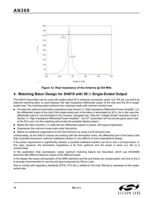
<strong>AN369</strong>Figure 12. Real Impedance of the <strong>Antenna</strong> @ 434 MHz4. <strong>Matching</strong> Balun Design for <strong>Si4010</strong> with 50 Single-Ended OutputThe <strong>Si4010</strong> transmitter can be used with single-ended 50 antennas (monopole, spiral, ILA, IFA etc.) as well if anexternal matching balun is used between the high impedance differential output of the chip <strong>and</strong> the 50 singleendedload. The matching balun performs four important tasks with minimal insertion loss:• Provides the optimum termination impedance (see Section “2. High Impedance Differential Power Amplifier” ) tothe differential output of the chip if the single-ended port of the balun is terminated by 50 . As in this case thedifferential output is not terminated in the complex conjugate way. (See the "voltage limited" operation mode inSection “2. High Impedance Differential Power Amplifier” ; the S11 parameter will not provide good return lossat the 50 port, but the matching will provide the possible highest power.)• Makes the balun function, i.e. adds the two differential outputs in-phase, with equal magnitudes.• Suppresses the common mode even-order harmonics.• Makes an additional suppression on the 2nd harmonic by using a 2nd harmonic trap.Unfortunately, as the <strong>Si4010</strong> outputs are working with the termination (here, the differential port of the balun) withhigh Q parallel resonance, optimum wideb<strong>and</strong> solution is very difficult or even impossible to design.If the power requirement is significantly relaxed, a possible wideb<strong>and</strong> solution can be to use a coil-type balun. Inthis case, however, the termination impedance is far from optimum <strong>and</strong> the power is lower (i.e, this is acompromise).In this application note narrowb<strong>and</strong>, nearly optimum matching baluns are described, which use 0402SMDelements with different element values at the different b<strong>and</strong>s.In the design the losses <strong>and</strong> parasitic of the SMD elements <strong>and</strong> the pcb traces are compensated, <strong>and</strong> due to this itis strongly recommended to use the pcb layout proposed by Silicon Labs.Also to comply with regulatory st<strong>and</strong>ards (ETSI, FCC etc.), additional 3rd order filtering is necessary at the singleendedside.14 Rev. 0.1