AN369: Si4010 Antenna Interface and Matching Network ... - wless.ru
AN369: Si4010 Antenna Interface and Matching Network ... - wless.ru
AN369: Si4010 Antenna Interface and Matching Network ... - wless.ru

You also want an ePaper? Increase the reach of your titles
YUMPU automatically turns print PDFs into web optimized ePapers that Google loves.
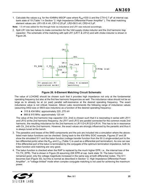
<strong>AN369</strong>1. Calculate the values e.g. for the 434MHz MSOP case where R AP =530 <strong>and</strong> the CTX=2.7 pF at internal cap.bank state of 19 (Table 1 in Section “2. High Impedance Differential Power Amplifier” ). The ideal matchingelement values are: LR1=35.4 nH, CR1=2.25 pF, LR2=58.5 nH, CR2=4.5 pF.Note: 1.5 nH was added for the through-hole via inductance <strong>and</strong> LR1 was reduced accordingly.2. Split LR1 into two halves to make connection for the Vdd supply choke inductor <strong>and</strong> the 2nd harmonic trapcapacitor. The schematic of the matching with split LR1 (LR11 & LR12) <strong>and</strong> with choke inductor is shown inFigure 26.Figure 26. 6-Element <strong>Matching</strong> Circuit SchematicThe value of LCHOKE should be chosen such that it provides high impedance not only at the fundamentaloperating frequency but also at the first few harmonic frequencies as well. The inductance value should not be solarge as to already be at (or past) parallel self-resonance at the desired operating frequency. The exactinductance value is not critical; however, Silicon Labs recommends the following range of inductance values(assuming 0402-size or 0603-size inductors) as a function of the desired operating frequency:•315 & 434 MHz: approximately 220..270 nH•868 & 915 MHz: approximately 120 nHThe value of the 2nd harmonic trap capacitor (Ctr_2nd) is chosen such that it is resonating in series with LR11<strong>and</strong> LR12 at the 2nd harmonic frequency. As LR11 <strong>and</strong> LR12 are parallel connected for the common mode 2ndharmonic, the resulting inductance for the 2nd harmonic is LR11/2=LR12/2=LR1/4. This has to be in resonancewith Ctr_2nd at the 2nd harmonic. However, the exact values are strongly influenced by the parasitic <strong>and</strong> thus itis always tuned at the bench.3. The parasitics <strong>and</strong> losses of the SMD components <strong>and</strong> the pcb are included into a simulation where the abovelistedmain balun functions can be checked. Going back to the 434 MHz SOIC example, Figures 27 <strong>and</strong> 28show the simulated S11 <strong>and</strong> the balun function (voltage transfer function from the 50 single-ended port to thetwo differential ports) when the R AP <strong>and</strong> C TX (Table 1) is used as a differential port termination). As one can seeif the differential port of the balun is terminated by the conjugate of the optimum termination impedance, both itsbalun function <strong>and</strong> matching are very good.4. The balun function is checked when the RAP is replaced by the much higher EPR, i.e., the internal loss of theTX (TX_EPR). That is shown in Figure 29 assuming 20K EPR at cap. bank state 19. The balun functionremained good, only the voltage magnitude increased in the same way at both differential nodes. The S11becomes bad (Figure 30), but this is normal as described in Section “2. High Impedance Differential PowerAmplifier” , in "voltage limited" mode when complex conjugate matching is not used for achieving the maximumpower.Rev. 0.1 25