Dissertation for the Degree of Master of Science in Engineering
Dissertation for the Degree of Master of Science in Engineering
Dissertation for the Degree of Master of Science in Engineering
- No tags were found...

Create successful ePaper yourself
Turn your PDF publications into a flip-book with our unique Google optimized e-Paper software.
<strong>Dissertation</strong> <strong>for</strong> <strong>the</strong> <strong>Degree</strong> <strong>of</strong> <strong>Master</strong> <strong>of</strong> <strong>Science</strong><strong>in</strong> Eng<strong>in</strong>eer<strong>in</strong>gClif<strong>for</strong>d Leonard van DykA dissertation submitted to <strong>the</strong> Department <strong>of</strong> Electrical Eng<strong>in</strong>eer<strong>in</strong>g,University <strong>of</strong> Cape Town, <strong>in</strong> fulfilment <strong>of</strong> <strong>the</strong> requirements<strong>for</strong> <strong>the</strong> degree <strong>of</strong> <strong>Master</strong> <strong>of</strong> <strong>Science</strong> <strong>in</strong> Eng<strong>in</strong>eer<strong>in</strong>g.Cape Town, 28 March 2002
DeclarationI declare that this dissertation is my own, unaided work. It is be<strong>in</strong>g submitted <strong>for</strong> <strong>the</strong>degree <strong>of</strong> <strong>Master</strong> <strong>of</strong> <strong>Science</strong> <strong>in</strong> Eng<strong>in</strong>eer<strong>in</strong>g at <strong>the</strong> University <strong>of</strong> Cape Town. It has notbeen submitted be<strong>for</strong>e <strong>for</strong> any degree or exam<strong>in</strong>ation at any o<strong>the</strong>r university.Signature <strong>of</strong> Author . . . . . . . . . . . . . . . . . . . . . . . . . . . . . . . . . . . . . . . . . . . . . . . . . . . . . . . . . . .Cape Town28 March 2002i
AbstractHistorically radio has been implemented us<strong>in</strong>g largely analogue circuitry. Improvements<strong>in</strong> mixed signal and digital signal process<strong>in</strong>g technology are rapidly lead<strong>in</strong>gtowards a largely digital approach, with down-conversion and filter<strong>in</strong>g mov<strong>in</strong>g to <strong>the</strong>digital signal process<strong>in</strong>g doma<strong>in</strong>. Advantages <strong>of</strong> this technology <strong>in</strong>clude <strong>in</strong>creasedper<strong>for</strong>mance and functionality, as well as reduced cost.Wideband receivers place <strong>the</strong> heaviest demands on both mixed signal and digital signalprocess<strong>in</strong>g technology, requir<strong>in</strong>g high spurious free dynamic range (SFDR) andsignal process<strong>in</strong>g bandwidths. This dissertation <strong>in</strong>vestigates <strong>the</strong> extent to which currentdigital technology is able to meet <strong>the</strong>se demands and compete with <strong>the</strong> provenarchitectures <strong>of</strong> analogue receivers. A scalable generalised digital radio receiver capable<strong>of</strong> operat<strong>in</strong>g <strong>in</strong> <strong>the</strong> HF and VHF bands was designed, implemented and tested,yield<strong>in</strong>g <strong>in</strong>stantaneous bandwidths <strong>in</strong> excess <strong>of</strong> 10 MHz with a spurious-free dynamicrange exceed<strong>in</strong>g 80 decibels below carrier (dBc).The results achieved reflect favourably on <strong>the</strong> digital receiver architecture. While <strong>the</strong>necessity <strong>for</strong> m<strong>in</strong>imal analogue circuitry will possibly always exist, digital radio architecturesare currently able to compete with analogue counterparts. The digital receiveris simple to manufacture, based on <strong>the</strong> use <strong>of</strong> largely commercial <strong>of</strong>f-<strong>the</strong>-shelf (COTS)components, and exhibits extreme flexibility and high per<strong>for</strong>mance when comparedwith comparably priced analogue receivers.ii
AcknowledgementsI wish to acknowledge and thank Peralex Electronics (Pty) Ltd. <strong>for</strong> <strong>the</strong> opportunity <strong>of</strong>present<strong>in</strong>g this project as a dissertation. In particular, <strong>the</strong> contributions <strong>of</strong> Glen Thiele,who has <strong>of</strong>fered unparalleled guidance, support and expertise are appreciated. I wouldalso like to thank Per Karlsen and Alex Bassios <strong>for</strong> <strong>the</strong>ir support and encouragement.I would like to thank Mark Cammidge <strong>for</strong> his assistance <strong>in</strong> pro<strong>of</strong>-read<strong>in</strong>g this dissertation.F<strong>in</strong>ally, I wish to thank my supervisor, Associate Pr<strong>of</strong>essor Michael Inggs, <strong>for</strong> hisguidance and support.iii
ContentsDeclarationAbstractAcknowledgementsContentsList <strong>of</strong> FiguresList <strong>of</strong> TablesList <strong>of</strong> AbbreviationsNomenclatureiiiiiiivviiixixiixiv1 Introduction 11.1 Background . . . . . . . . . . . . . . . . . . . . . . . . . . . . . . . 21.2 Scope . . . . . . . . . . . . . . . . . . . . . . . . . . . . . . . . . . 21.3 System Specification . . . . . . . . . . . . . . . . . . . . . . . . . . 41.4 System Architecture . . . . . . . . . . . . . . . . . . . . . . . . . . . 51.5 Related Work . . . . . . . . . . . . . . . . . . . . . . . . . . . . . . 61.6 Document Overview . . . . . . . . . . . . . . . . . . . . . . . . . . 72 Wideband Signal Digitisation 82.1 Dynamic Range Restrictions <strong>in</strong> Wideband Digitisation . . . . . . . . 82.2 Bandpass Sampl<strong>in</strong>g Theory . . . . . . . . . . . . . . . . . . . . . . . 112.2.1 Nyquist’s Criterion . . . . . . . . . . . . . . . . . . . . . . . 112.2.2 Bandpass Sampl<strong>in</strong>g . . . . . . . . . . . . . . . . . . . . . . . 112.2.3 Spectral Inversion <strong>in</strong> Bandpass Sampl<strong>in</strong>g . . . . . . . . . . . 142.2.4 Apply<strong>in</strong>g Bandpass Sampl<strong>in</strong>g to Wideband Reception . . . . 142.2.5 Quadrature Sampl<strong>in</strong>g and Complex Signal Representation . . 15iv
2.3 Sources <strong>of</strong> Error <strong>in</strong> Wideband Digitisation . . . . . . . . . . . . . . . 162.3.1 Quantisation Error . . . . . . . . . . . . . . . . . . . . . . . 172.3.2 Static Errors <strong>in</strong> <strong>the</strong> A-D Transfer Function . . . . . . . . . . . 172.3.3 Sampl<strong>in</strong>g Jitter . . . . . . . . . . . . . . . . . . . . . . . . . 192.3.4 Relative Noise Contributions <strong>in</strong> Wideband Digitisation . . . . 212.4 Oversampl<strong>in</strong>g . . . . . . . . . . . . . . . . . . . . . . . . . . . . . . 222.4.1 Relaxation <strong>of</strong> Anti-alias<strong>in</strong>g Filter Requirements . . . . . . . . 232.4.2 Signal-to-Noise Ratio Improvement Through Oversampl<strong>in</strong>g . 232.4.3 Spurious Harmonic Placement . . . . . . . . . . . . . . . . . 242.5 Signal Di<strong>the</strong>r<strong>in</strong>g . . . . . . . . . . . . . . . . . . . . . . . . . . . . . 242.5.1 Subtractive and Non-subtractive Di<strong>the</strong>r<strong>in</strong>g Techniques . . . . 252.5.2 Small- and Large-scale Di<strong>the</strong>r<strong>in</strong>g . . . . . . . . . . . . . . . 272.6 A-D Converter Input Level Match<strong>in</strong>g . . . . . . . . . . . . . . . . . . 292.6.1 Characteristics <strong>of</strong> an Analogue Receiver Cha<strong>in</strong> . . . . . . . . 292.6.2 Comb<strong>in</strong>ed Analogue and A-D Converter Noise Figure . . . . 312.6.3 Optimal Analogue and A-D Converter Interfac<strong>in</strong>g . . . . . . . 312.7 Selection <strong>of</strong> a Wideband A-D Converter . . . . . . . . . . . . . . . . 322.7.1 A-D Converter Architectures . . . . . . . . . . . . . . . . . . 332.7.2 Survey <strong>of</strong> Commercially Available Wideband A-D Converters 332.7.3 Comparison <strong>of</strong> AD6644 and CLC5958 . . . . . . . . . . . . 343 Digital Down-conversion and Multirate Signal Process<strong>in</strong>g 373.1 A Generalised IF Sampl<strong>in</strong>g Receiver Architecture . . . . . . . . . . . 383.2 Spectral Translation <strong>of</strong> IFs to Baseband . . . . . . . . . . . . . . . . 383.2.1 Spectral translation through quadrature digital mix<strong>in</strong>g . . . . 393.2.2 Hardware-Efficient Frequency Translation . . . . . . . . . . . 403.2.3 Per<strong>for</strong>mance Advantages <strong>of</strong> Digital Spectral Translation . . . 403.3 Digital Resampl<strong>in</strong>g and Multirate Signal Process<strong>in</strong>g . . . . . . . . . . 413.3.1 Decimation by Integer Factors . . . . . . . . . . . . . . . . . 413.3.2 Interpolation by Integer Factors . . . . . . . . . . . . . . . . 423.3.3 Resampl<strong>in</strong>g by Non-Integer Factors . . . . . . . . . . . . . . 433.3.4 Efficient Architectures <strong>for</strong> Integer Decimation . . . . . . . . . 443.3.5 Enhanced Signal-to-Noise Ratio through Decimation Filter<strong>in</strong>g 483.4 Enhanced Signal-to-Noise Ratio us<strong>in</strong>g <strong>the</strong> Discrete Fourier Trans<strong>for</strong>m 484 Wideband Digital Receiver Architecture and Design 504.1 Overview <strong>of</strong> System Architecture . . . . . . . . . . . . . . . . . . . . 504.2 Digital Receiver Channel Architecture . . . . . . . . . . . . . . . . . 514.2.1 A Review <strong>of</strong> <strong>the</strong> Digital Receiver Requirements . . . . . . . . 524.2.2 Commercially Available Digital Down-conversion Hardware . 534.2.3 A Scalable Digital Receiver based on COTS components . . . 55v
4.2.4 A Description <strong>of</strong> <strong>the</strong> ADC-DDC Board Architecture . . . . . 594.2.5 A Description <strong>of</strong> <strong>the</strong> ISA DSP Board Architecture . . . . . . 645 Digital Receiver Implementation 675.1 A-D Converter Input Level Match<strong>in</strong>g . . . . . . . . . . . . . . . . . . 675.2 A-D Converter Input Signal Di<strong>the</strong>r<strong>in</strong>g . . . . . . . . . . . . . . . . . 685.3 Selection <strong>of</strong> a Sampl<strong>in</strong>g Oscillator . . . . . . . . . . . . . . . . . . . 695.4 Analogue Power Supply Filter<strong>in</strong>g . . . . . . . . . . . . . . . . . . . . 705.5 Ground<strong>in</strong>g . . . . . . . . . . . . . . . . . . . . . . . . . . . . . . . . 715.6 EMI Shield<strong>in</strong>g . . . . . . . . . . . . . . . . . . . . . . . . . . . . . . 715.7 GC4016 Decimat<strong>in</strong>g Filter Coefficients . . . . . . . . . . . . . . . . 725.8 Problems Encountered dur<strong>in</strong>g Receiver Design . . . . . . . . . . . . 735.8.1 Insufficient EMI Suppression . . . . . . . . . . . . . . . . . 735.8.2 Problems due to Faulty Silicon . . . . . . . . . . . . . . . . . 746 Per<strong>for</strong>mance Measurements 756.1 Empirical Test<strong>in</strong>g <strong>of</strong> A-D Converter and Analogue Front-End Circuitry 756.1.1 Non-harmonic Spurious Free Dynamic Range . . . . . . . . . 756.1.2 Harmonic Spurious Free Dynamic Range . . . . . . . . . . . 766.1.3 Effect <strong>of</strong> Band-limited Di<strong>the</strong>r Noise on A-D Converter L<strong>in</strong>earity 776.2 Empirical Test<strong>in</strong>g <strong>of</strong> <strong>the</strong> Digital Receiver at 5 MHz IF . . . . . . . . . 776.2.1 Non-harmonic Spurious-free Dynamic Range . . . . . . . . . 786.2.2 Harmonic Spurious-free Dynamic Range . . . . . . . . . . . 786.2.3 Two-tone Third-order Intermodulation Distortion Measurement 786.3 Empirical Test<strong>in</strong>g <strong>of</strong> <strong>the</strong> Digital Receiver at 12.8 MHz IF . . . . . . . 806.3.1 Non-Harmonic Spurious-free Dynamic Range . . . . . . . . . 806.3.2 Harmonic Spurious-free Dynamic Range . . . . . . . . . . . 816.3.3 Two-tone Third-order Intermodulation Distortion Measurement 827 Conclusion 84Bibliography 87A Derivations 90A.1 Signal-to-Noise Ratio result<strong>in</strong>g from Encode Jitter . . . . . . . . . . . 90B GC4016 Wideband Decimation Filter<strong>in</strong>g Frequency Response 92C Digital Receiver Per<strong>for</strong>mance Plots 99C.1 AD6644 A-D Converter Output Plots . . . . . . . . . . . . . . . . . . 99C.2 Wideband 5 MHz IF 800 kHz Bandwidth Receiver Output Plots . . . 99C.3 Wideband 12.8 MHz IF 10 MHz Bandwidth Receiver Output Plots . . 100vi
D System and Board Physical Construction and Layout 114vii
List <strong>of</strong> Figures1.1 The progression <strong>of</strong> receivers from analogue to digital . . . . . . . . . 32.1 An example plot <strong>of</strong> maximum bandwidth versus number <strong>of</strong> bits. . . . 102.2 A typical bandpass sampl<strong>in</strong>g scheme . . . . . . . . . . . . . . . . . . 122.3 The allowed regions <strong>for</strong> bandpass sampl<strong>in</strong>g . . . . . . . . . . . . . . 132.4 Illustration <strong>of</strong> quadrature sampl<strong>in</strong>g scheme. . . . . . . . . . . . . . . 152.5 The voltage error result<strong>in</strong>g from encode signal jitter . . . . . . . . . . 202.6 Signal-to-noise ratio versus analogue <strong>in</strong>put frequency <strong>for</strong> <strong>the</strong> AD6644. 222.7 Anti-alias<strong>in</strong>g filter transition width requirements . . . . . . . . . . . . 232.8 Band placement such that harmonics do not fall <strong>in</strong>-band after digitisation.. . . . . . . . . . . . . . . . . . . . . . . . . . . . . . . . . . . 242.9 Subtractive and non-subtractive di<strong>the</strong>r<strong>in</strong>g schemes . . . . . . . . . . . 263.1 A generalised IF-sampl<strong>in</strong>g digital receiver. . . . . . . . . . . . . . . . 383.2 The quadrature digital mix<strong>in</strong>g process. . . . . . . . . . . . . . . . . . 393.3 Decimation by an <strong>in</strong>teger factor M=4. . . . . . . . . . . . . . . . . . 423.4 Interpolation by an <strong>in</strong>teger factor M=4. . . . . . . . . . . . . . . . . . 443.5 Resampl<strong>in</strong>g by a rational factorM L . . . . . . . . . . . . . . . . . . . . 453.6 Halfband filter frequency response. . . . . . . . . . . . . . . . . . . . 453.7 Structure <strong>of</strong> a CIC decimat<strong>in</strong>g filter. . . . . . . . . . . . . . . . . . . 463.8 Structure <strong>of</strong> a CIC decimat<strong>in</strong>g filter. . . . . . . . . . . . . . . . . . . 47viii
4.1 Typical wideband surveillance receiver system configuration. . . . . . 504.2 Block diagram <strong>of</strong> <strong>the</strong> GC4016 quad digital down-converter . . . . . . 554.3 Adjacent narrowband channels used to <strong>for</strong>m a wideband output. . . . 584.4 Block diagram <strong>of</strong> <strong>the</strong> A-D Converter board. . . . . . . . . . . . . . . 604.5 Block diagram <strong>of</strong> <strong>the</strong> digital down-converter board. . . . . . . . . . . 614.6 Block diagram <strong>of</strong> <strong>the</strong> general purpose ISA-based DSP card. . . . . . . 666.1 Test setup <strong>for</strong> harmonic spurious per<strong>for</strong>mance measurement. . . . . . 776.2 Intermodulation distortion test setup. . . . . . . . . . . . . . . . . . . 806.3 S<strong>in</strong>gle-tone harmonic spurious-free dynamic range versus frequency. . 816.4 S<strong>in</strong>gle-tone harmonic spurious-free dynamic range versus <strong>in</strong>put amplitude.. . . . . . . . . . . . . . . . . . . . . . . . . . . . . . . . . 82B.1 Magnitude and phase response <strong>of</strong> 5th order CIC decimation filter (decimateby 8). . . . . . . . . . . . . . . . . . . . . . . . . . . . . . . . 93B.2 Magnitude and phase response <strong>of</strong> 21-tap CFIR FIR filter. . . . . . . . 94B.3 Comb<strong>in</strong>ed magnitude and phase response <strong>of</strong> CIC and CFIR. . . . . . 95B.4 Magnitude and phase response <strong>of</strong> 63-tap PFIR FIR filter. . . . . . . . 96B.5 Comb<strong>in</strong>ed magnitude and phase response <strong>of</strong> CFIR and PFIR filters. . 97B.6 Comb<strong>in</strong>ed magnitude and phase response <strong>of</strong> CIC, CFIR and PFIR filters. 98C.1 Receiver analogue <strong>in</strong>put term<strong>in</strong>ated <strong>in</strong> 50 Ω. . . . . . . . . . . . . . . 100C.2 7.6 MHz, -1 dBFS tone at receiver analogue <strong>in</strong>put. . . . . . . . . . . 101C.3 7.6 MHz, -30 dBFS tone at receiver analogue <strong>in</strong>put with no di<strong>the</strong>r. . . 102C.4 7.6 MHz, -30 dBFS tone at receiver analogue <strong>in</strong>put with di<strong>the</strong>r. . . . . 103C.5 S<strong>in</strong>gle tone at 5.15 MHz <strong>of</strong> amplitude -1 dBFS (averaged). . . . . . . 104C.6 S<strong>in</strong>gle tone at 5.15 MHz <strong>of</strong> amplitude -1 dBFS (peak hold). . . . . . . 105C.7 Two-tone <strong>in</strong>termodulation test results at 5 MHz IF (averaged). . . . . 106ix
C.8 Two-tone <strong>in</strong>termodulation test results at 5 MHz IF(peak hold) . . . . . 107C.9 Receiver <strong>in</strong>put term<strong>in</strong>ated <strong>in</strong> 50 Ω (averaged). . . . . . . . . . . . . . 108C.10 Receiver <strong>in</strong>put term<strong>in</strong>ated <strong>in</strong> 50 Ω (peak hold). . . . . . . . . . . . . 109C.11 S<strong>in</strong>gle tone at 12.64 MHz, -1 dBFS (averaged). . . . . . . . . . . . . 110C.12 S<strong>in</strong>gle tone at 12.64 MHz, -1 dBFS (peak hold). . . . . . . . . . . . . 111C.13 Two-tone <strong>in</strong>termodulation test results at 12.8 MHz IF (averaged). . . . 112C.14 Two-tone <strong>in</strong>termodulation test results at 12.8 MHz IF (peak hold). . . 113D.1 6-Antenna wideband receiver <strong>in</strong>corporat<strong>in</strong>g <strong>the</strong> digital receiver. . . . . 114D.2 6-Channel wideband digital receiver. . . . . . . . . . . . . . . . . . . 116D.3 Physical layout <strong>of</strong> <strong>the</strong> digital receiver adapter card and mezzan<strong>in</strong>emodule. . . . . . . . . . . . . . . . . . . . . . . . . . . . . . . . . . 117D.4 Physical layout <strong>of</strong> <strong>the</strong> ADC and DDC boards. . . . . . . . . . . . . . 118D.5 Assembled digital receiver card (no shield<strong>in</strong>g cover). . . . . . . . . . 118x
List <strong>of</strong> Tables1.1 Wideband receiver operat<strong>in</strong>g mode requirements . . . . . . . . . . . 52.1 Parameters used <strong>in</strong> <strong>the</strong> calculation <strong>of</strong> maximum sampled bandwidth . 102.2 A comparison <strong>of</strong> <strong>the</strong> AD6644 and CLC5958 A-D converters . . . . . 364.1 Commercially available ASICs <strong>for</strong> digital down-conversion . . . . . . 545.1 Parameters used <strong>in</strong> <strong>the</strong> calculation <strong>of</strong> oscillator jitter. . . . . . . . . . 70D.1 Key <strong>for</strong> figure D.1 . . . . . . . . . . . . . . . . . . . . . . . . . . . . 115D.2 Key <strong>for</strong> figure D.2 . . . . . . . . . . . . . . . . . . . . . . . . . . . . 115D.3 Key <strong>for</strong> figure D.3 . . . . . . . . . . . . . . . . . . . . . . . . . . . . 115D.4 Key <strong>for</strong> figure D.4 . . . . . . . . . . . . . . . . . . . . . . . . . . . . 117xi
List <strong>of</strong> AbbreviationsADC— Analogue-to-digital converterAGC— Automatic ga<strong>in</strong> controlASIC— Application-specific <strong>in</strong>tegrated circuitcf— Characteristic functionCIC— Cascaded <strong>in</strong>tegrator-combCOTS— Commercial <strong>of</strong>f-<strong>the</strong>-shelfCPLD— Complex programmable logic deviceDAC— Digital-to-analogue converterdBc— Decibels relative to carrierdBFS— Decibels relative to full-scaleDDC— Digital down-converterDDS— Digital signal syn<strong>the</strong>sisDF— Direction f<strong>in</strong>d<strong>in</strong>gDFT— Discrete Fourier Trans<strong>for</strong>mDMA— Direct memory accessDNL— Differential non-l<strong>in</strong>earityDUT— Device under testFFT— Fast Fourier Trans<strong>for</strong>mFIR— F<strong>in</strong>ite impulse responsexii
FPGA— Field-programmable gate arrayFSR— Full-scale rangeIF— Intermediate frequencyIM3— Third-order <strong>in</strong>termodulation productsINL— Integral non-l<strong>in</strong>earityIP3— Third-order <strong>in</strong>tercept po<strong>in</strong>tISA— Industrial Standard ArchitectureLO— Local oscillatorLSB— Least significant bitMDS— M<strong>in</strong>imum discernable signalMGC— Manual ga<strong>in</strong> controlMSB— Most significant bitNCO— Numerically controlled oscillatorNSD— Non-subtractive di<strong>the</strong>rpdf— Probability density functionRPDF— Rectangular probability density functionSBC— S<strong>in</strong>gle board computerSD— Subtractive di<strong>the</strong>rSDR— S<strong>of</strong>tware def<strong>in</strong>ed radioSIMD— S<strong>in</strong>gle <strong>in</strong>struction multiple dataSINAD— Signal-to-noise-and-distortionSFDR— Spurious-free dynamic rangeSNR— Signal-to-noise ratioSSB— S<strong>in</strong>gle side bandTDOA— Time difference <strong>of</strong> arrivalxiii
NomenclatureBand Occupancy— The band occupancy is usually expressed as a percentage andis def<strong>in</strong>ed as <strong>the</strong> ratio <strong>of</strong> <strong>the</strong> number <strong>of</strong> signals present with<strong>in</strong> a particular band-<strong>of</strong><strong>in</strong>terestto <strong>the</strong> number <strong>of</strong> available channels allocated to <strong>the</strong> band.Noise Factor— The noise factor (NF) provides a measure <strong>of</strong> <strong>the</strong> contribution <strong>of</strong> <strong>in</strong>herent(<strong>in</strong>ternal) device noise on total system noise. It is def<strong>in</strong>ed as <strong>the</strong> ratio <strong>of</strong> <strong>the</strong>signal-to-noise ratio (SNR) measured at <strong>the</strong> device output and <strong>the</strong> SNR ratio measuredat <strong>the</strong> device <strong>in</strong>put under normal operat<strong>in</strong>g conditions. By convention, it is expressed<strong>in</strong> a dB scale.Selectivity—The property <strong>of</strong> a receiver that allows it to dist<strong>in</strong>guish between signals atdifferent frequencies.Sensitivity—For sufficiently high levels <strong>of</strong> receiver ga<strong>in</strong>, <strong>the</strong> weakest signal powerthat may be acceptably processed is limited by noise. This signal level is referred toas <strong>the</strong> sensitivity <strong>of</strong> <strong>the</strong> system and varies with external noise level.Spurious Free Dynamic Range (SFDR)—The ratio <strong>of</strong> <strong>the</strong> peak RMS signal amplitudeto <strong>the</strong> RMS value <strong>of</strong> <strong>the</strong> peak spurious spectral component. This may or may notbe a harmonic. It is usually expressed <strong>in</strong> decibels relative to carrier (dBc) or decibelsrelative to full scale (dBFS), and it is <strong>the</strong>re<strong>for</strong>e important to pay attention to <strong>the</strong> units<strong>of</strong> measurement.xiv
Chapter 1IntroductionDigital radio implementations are <strong>in</strong>creas<strong>in</strong>gly be<strong>in</strong>g adopted. Analogue circuitry israpidly be<strong>in</strong>g replaced by digital signal process<strong>in</strong>g (DSP), analogue-to-digital (A-D)and digital-to-analogue (D-A) conversion. Advantages <strong>of</strong> this technology <strong>in</strong>clude <strong>in</strong>creasedper<strong>for</strong>mance and functionality, and reduced cost. Dedicated analogue circuitrymay be replaced by flexible, robust DSP application-specific <strong>in</strong>tegrated circuits(ASICs) and s<strong>of</strong>tware.Analogue-to-digital conversion technology currently limits <strong>the</strong> <strong>in</strong>stantaneous energythat may be received, as a result <strong>of</strong> limited A-D converter dynamic range. If <strong>the</strong>received energy is widely distributed over <strong>the</strong> received spectrum (usually a valid assumptiongiven <strong>the</strong> typical energy spread <strong>in</strong> <strong>the</strong> bands <strong>of</strong> <strong>in</strong>terest), <strong>the</strong> bandwidth thatmay be received at any given level <strong>of</strong> available dynamic range is limited. Cont<strong>in</strong>uoustechnological advances move closer to <strong>the</strong> ideal <strong>of</strong> connect<strong>in</strong>g an A-D converter(ADC) directly to a bandwidth-limited antenna, and directly sampl<strong>in</strong>g wide RF spectrawith sufficient dynamic range to permit <strong>the</strong> demodulation <strong>of</strong> narrowband channelsus<strong>in</strong>g digital signal process<strong>in</strong>g hardware and s<strong>of</strong>tware. Digitisation <strong>of</strong> <strong>the</strong> entire HFspectrum (2-30 MHz) has recently become feasible, with state-<strong>of</strong>-<strong>the</strong>-art A-D converterscurrently capable <strong>of</strong> sampl<strong>in</strong>g rates <strong>of</strong> up to 105 MSPS at 14 bit resolution. Digitalsignal process<strong>in</strong>g hardware and algorithm speeds, once considered an impediment to<strong>the</strong> digitisation <strong>of</strong> wideband data, cont<strong>in</strong>ue to advance and are currently capable <strong>of</strong>per<strong>for</strong>m<strong>in</strong>g advanced signal process<strong>in</strong>g tasks, such as adaptive equalisation, which aredifficult or impossible to implement <strong>in</strong> <strong>the</strong> analogue doma<strong>in</strong>.This dissertation explores <strong>the</strong> digitisation and frontend digital signal process<strong>in</strong>g <strong>of</strong> <strong>the</strong>HF and VHF spectra <strong>for</strong> <strong>the</strong> purposes <strong>of</strong> wideband radio reception.1
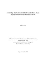
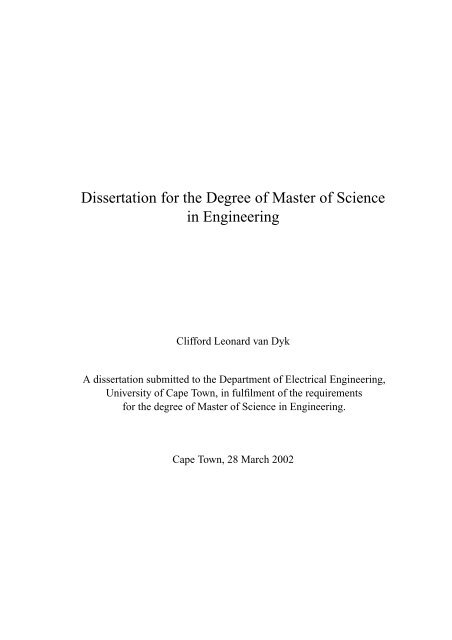
1.1 BackgroundA well-documented history <strong>of</strong> communications receivers can be found <strong>in</strong> Rohde etal. [23]. The development <strong>of</strong> <strong>the</strong> superheterodyne-type receivers revolutionised receiverdesign, relegat<strong>in</strong>g previous receiver architectures to occasional, special-purposeuse. The superheterodyne architecture is not without problems, however. The use <strong>of</strong>mixers to per<strong>for</strong>m frequency translation <strong>in</strong>troduces <strong>the</strong> associated problems <strong>of</strong> imagefrequency rejection, IF leak-through and high order non-l<strong>in</strong>earities. Local oscillator(LO) noise sidebands may be translated to <strong>the</strong> IF by a strong out-<strong>of</strong>-band signal(usually a strong adjacent channel), a process termed reciprocal mix<strong>in</strong>g[23]. Phaseimbalance between <strong>in</strong>-phase and quadrature channels significantly limits per<strong>for</strong>mance<strong>in</strong> analogue quadrature channel conversion[27].The advantages <strong>of</strong> a digital receiver solution are significant, and <strong>in</strong>clude reduced systemcost, <strong>in</strong>creased temperature stability, f<strong>in</strong>er tun<strong>in</strong>g resolution, faster tun<strong>in</strong>g speed,excellent quadrature channel phase balance, <strong>in</strong>creased filter selectivity, robustness <strong>in</strong>terms <strong>of</strong> both hardware and s<strong>of</strong>tware signal process<strong>in</strong>g algorithms, reconfigurability,advanced signal process<strong>in</strong>g techniques and <strong>the</strong> ability to store signals <strong>for</strong> subsequent<strong>of</strong>f-l<strong>in</strong>e process<strong>in</strong>g.These benefits have resulted <strong>in</strong> <strong>the</strong> digitisation process mov<strong>in</strong>g closer to <strong>the</strong> RF frontend,with <strong>the</strong> ultimate goal <strong>of</strong> directly digitis<strong>in</strong>g <strong>the</strong> antenna output. The “S<strong>of</strong>twareDef<strong>in</strong>ed Radio” (SDR) has recently been realised, allow<strong>in</strong>g reconfiguration <strong>of</strong> signalprocess<strong>in</strong>g functions through s<strong>of</strong>tware, and result<strong>in</strong>g <strong>in</strong> reconfigurable radios capable<strong>of</strong> operat<strong>in</strong>g over multiple air <strong>in</strong>terfaces.Figure 1.1 illustrates <strong>the</strong> progression <strong>of</strong> receivers <strong>in</strong> recent years. Initially, <strong>the</strong> limitedsample rates <strong>of</strong> A-D converters and limited digital signal process<strong>in</strong>g power precluded<strong>the</strong> use <strong>of</strong> digital hardware beyond baseband signals. With recent improvements <strong>in</strong>A-D conversion and digital signal process<strong>in</strong>g hardware, sampl<strong>in</strong>g and process<strong>in</strong>g <strong>of</strong>wideband IF signals has become a reality. Digital down-conversion has facilitated<strong>the</strong> elim<strong>in</strong>ation <strong>of</strong> analogue down-conversion and quadrature conversion stages. It islikely that future digital and mixed signal technology will soon supersede <strong>the</strong> superheterodynearchitecture completely, directly sampl<strong>in</strong>g bandlimited RF signals.1.2 ScopeThis dissertation is an <strong>in</strong>vestigation and evaluation <strong>of</strong> state-<strong>of</strong>-<strong>the</strong>-art wideband digitalradio receiver hardware through <strong>the</strong> design, implementation and qualification <strong>of</strong> ascalable multi-channel IF-<strong>in</strong>put wideband digital radio receiver. A survey <strong>of</strong> digital2
Analog ReceiverAudioSpectralAnalysisDFetc.BasebandAnalog Down-converterfDigitalReceiverAudioSpectralAnalysisDFetc.IFAnalog Down-converterfDigitalReceiverAudioSpectralAnalysisDFetc.Digital ReceiverAudioSpectralAnalysisDFetc. ?Figure 1.1: The progression <strong>of</strong> receivers from analogue to digital3
adio receiver architectures and relevant <strong>the</strong>ory is conducted. Simulations and empirical<strong>in</strong>vestigations are per<strong>for</strong>med. A general-purpose wideband digital receiver capable<strong>of</strong> operat<strong>in</strong>g <strong>in</strong> <strong>the</strong> HF and VHF bands is proposed and implemented. The receiver isquantitatively evaluated, after which conclusions on receiver per<strong>for</strong>mance and futuretrends <strong>in</strong> wideband digital radio architectures are drawn.The design, implementation and qualification <strong>of</strong> <strong>the</strong> general-purpose receiver spans atwo-year period dur<strong>in</strong>g which <strong>the</strong> author was solely responsible <strong>for</strong> <strong>the</strong> design, test<strong>in</strong>gand <strong>in</strong>tegration <strong>of</strong> digital receiver hardware and driver-level s<strong>of</strong>tware <strong>in</strong> numeroussystems.1.3 System SpecificationThe design goal <strong>for</strong> <strong>the</strong> system is to realise a highly reconfigurable digital receiverus<strong>in</strong>g commercial-<strong>of</strong>f-<strong>the</strong>-shelf (COTS) components where possible.• The receiver should be capable <strong>of</strong> function<strong>in</strong>g as a backend to wideband andnarrowband analogue down-converters.• It should be capable <strong>of</strong> digitis<strong>in</strong>g <strong>the</strong> <strong>in</strong>termediate frequency (IF) output <strong>of</strong> analoguedown-converters with output bandwidths <strong>of</strong> up to 10 MHz, at IF’s <strong>in</strong> <strong>the</strong>HF and VHF bands.• The receiver should accept full scale s<strong>in</strong>gle-ended analogue <strong>in</strong>put signal levels<strong>of</strong> ca. 0 dBm, with allowance <strong>for</strong> fixed amplification <strong>of</strong> 20 dB. It is presumedthat any dynamic analogue receiver ga<strong>in</strong> (manual or automatic ga<strong>in</strong> control) thatmay exist is <strong>in</strong>cluded <strong>in</strong> <strong>the</strong> analogue down-converter.• The receiver is required to support wideband down-conversion, baseband filter<strong>in</strong>gand rate reduction <strong>in</strong> hardware.• It should fur<strong>the</strong>r support <strong>the</strong> extraction <strong>of</strong> narrowband signals from <strong>the</strong> wideband<strong>in</strong>put <strong>for</strong> <strong>the</strong> purpose <strong>of</strong> real-time demodulation.• The system should be scalable, support<strong>in</strong>g multiple receiver channels.• It should conta<strong>in</strong> flexible sampl<strong>in</strong>g and synchronisation circuitry to supportphase-synchronous data acquisition on multiple channels, a prerequisite <strong>in</strong> applicationssuch as wideband direction f<strong>in</strong>d<strong>in</strong>g (DF) and beam<strong>for</strong>m<strong>in</strong>g.The required modes <strong>of</strong> operation are presented <strong>in</strong> table 1.1.4
Sampl<strong>in</strong>g IF Input Output SFDR MaximumFrequency Bandwidth Bandwidth Channel Count51.2 MSPS 5.0 MHz 800 kHz 800 kHz 80 dBc 5 (synch)51.2 MSPS 12.8 MHz 10 MHz 10 MHz 75 dBc 6 (synch)51.2 MSPS 5.0 MHz 500 kHz 11 kHz 80 dBc 12 (asynch)Table 1.1: Wideband receiver operat<strong>in</strong>g mode requirements1.4 System ArchitectureThe receiver implementation consists <strong>of</strong> one (s<strong>in</strong>gle antenna) or more (multiple antenna)wideband receiver channels implemented on full-length PC ISA adapter cardsand mezzan<strong>in</strong>e modules and mounted <strong>in</strong> a ruggedised <strong>in</strong>dustrial comput<strong>in</strong>g rack. Acommercially available <strong>in</strong>dustrial S<strong>in</strong>gle Board Computer (SBC) hous<strong>in</strong>g s<strong>in</strong>gle ordual Intel Pentium processors with 100 Mbit e<strong>the</strong>rnet support <strong>for</strong>ms <strong>the</strong> ma<strong>in</strong> systemcontroller and high-per<strong>for</strong>mance back-end processor <strong>for</strong> <strong>the</strong> system. It fur<strong>the</strong>rallows <strong>the</strong> system to act as a networked data server sub-system on larger systems, support<strong>in</strong>gsystem growth. The implemented hardware facilitates multi-channel phasesynchronousdata acquisition.Each wideband receiver (ISA adapter card and mezzan<strong>in</strong>e boards) conta<strong>in</strong>s m<strong>in</strong>imalanalogue signal condition<strong>in</strong>g circuitry, a wideband 14 bit 65/80 MSPS A-D converter,dedicated digital down-conversion (DDC) signal process<strong>in</strong>g hardware, extensiveFIFO buffer<strong>in</strong>g and an Analog Devices ADSP-21160 Super Harvard Architecturefloat<strong>in</strong>g-po<strong>in</strong>t digital signal processor (DSP). The SBC communicates directlywith <strong>the</strong> DSP via <strong>the</strong> DSP’s host processor <strong>in</strong>terface which is accessible to <strong>the</strong> SBCon <strong>the</strong> ISA bus. Sample tim<strong>in</strong>g and synchronisation circuitry may be implementedon-board (asynchronous/stand-alone receivers) or generated externally (synchronousmulti-channel receivers).An important design decision is <strong>the</strong> approach taken to realise wide <strong>in</strong>stantaneousbandwidths necessary <strong>for</strong> fast scann<strong>in</strong>g receivers and wideband DF applications. Awide <strong>in</strong>stantaneous bandwidth is <strong>for</strong>med from multiple digital down-conversion channelstuned to adjacent bands. This approach provides a scalable solution to achiev<strong>in</strong>gboth narrow and wide output bandwidths while ma<strong>in</strong>ta<strong>in</strong><strong>in</strong>g efficient down-conversionstructures and <strong>in</strong>creased signal process<strong>in</strong>g ga<strong>in</strong>. A limitation <strong>of</strong> this approach is that<strong>the</strong> wideband data is channelised, mak<strong>in</strong>g subsequent narrowband time doma<strong>in</strong> process<strong>in</strong>g<strong>of</strong> <strong>the</strong> wideband data difficult.Each digital receiver board may <strong>for</strong>m <strong>the</strong> back-end to a wideband analogue receiveror may be configured to sample a bandwidth-limited antenna <strong>in</strong>put directly. The re-5
ceiver’s analogue <strong>in</strong>put bandwidth may extend to 250 MHz (sub-Nyquist sampl<strong>in</strong>g),allow<strong>in</strong>g <strong>the</strong> receiver to operate <strong>in</strong> <strong>the</strong> HF and VHF bands, while support<strong>in</strong>g <strong>in</strong>stantaneousoutput bandwidths <strong>in</strong> excess <strong>of</strong> 10 MHz.Much consideration was given to <strong>the</strong> qualification <strong>of</strong> receiver boards dur<strong>in</strong>g systemdesign. Test modes were <strong>in</strong>corporated <strong>in</strong>to <strong>the</strong> hardware design, such that <strong>the</strong> receiverper<strong>for</strong>mance could be fully evaluated.Firmware was written <strong>in</strong> VHDL and was compiled us<strong>in</strong>g Altera Max+Plus II s<strong>of</strong>tware.Test s<strong>of</strong>tware operat<strong>in</strong>g on <strong>the</strong> ADSP-21160 DSP was developed us<strong>in</strong>g <strong>the</strong> AnalogDevices Inc. VisualDSP++ C/C++ V1.0 compiler and development suite. Host CPUs<strong>of</strong>tware was developed us<strong>in</strong>g <strong>the</strong> Micros<strong>of</strong>t Visual C++ 6.0 compiler and developmentplat<strong>for</strong>m. W<strong>in</strong>DK DDK Development Library V2.7 was used <strong>in</strong> conjunctionwith <strong>the</strong> W<strong>in</strong>dows Plat<strong>for</strong>m SDK and W<strong>in</strong>dows NT4.0 DDK <strong>in</strong> <strong>the</strong> development <strong>of</strong>device driver s<strong>of</strong>tware <strong>for</strong> communicat<strong>in</strong>g with <strong>the</strong> ISA adapter cards. Simulationswere per<strong>for</strong>med under MATLAB 5.2.1.5 Related WorkCurrent research ef<strong>for</strong>ts focus on improv<strong>in</strong>g both converter speed and l<strong>in</strong>earity.Velazquez[29] decribes a technique that may improve <strong>the</strong> speed <strong>of</strong> conversion <strong>of</strong> highspeed,high resolution analog-to-digital converters <strong>in</strong> RF receiver applications by upto six times <strong>the</strong> state-<strong>of</strong>-<strong>the</strong>-art us<strong>in</strong>g a filter bank architecture.Sigma-delta techniques promise to provide high-resolution A-D converters capable <strong>of</strong>sampl<strong>in</strong>g narrowband signals at a sampl<strong>in</strong>g frequency range that extends to gigahertz[14].Post-digitisation error correction schemes aim to reduce <strong>the</strong> non-l<strong>in</strong>earities <strong>in</strong> <strong>the</strong> digitisationprocess by modell<strong>in</strong>g <strong>the</strong> error mechanisms <strong>in</strong>herent <strong>in</strong> A-D conversion. A-Dconversion error has been shown to be related to analogue <strong>in</strong>put frequency, and staticerror correction is giv<strong>in</strong>g way to dynamic correction schemes such as phase-planecompensation[9], s<strong>in</strong>ewave histogram compensation [15] and adaptive compensation[18]. A-D converter non-l<strong>in</strong>earities have been reduced by as much as 10 to 20 dBus<strong>in</strong>g <strong>the</strong>se techniques.6
1.6 Document OverviewChapter 1 provides an overview <strong>of</strong> this dissertation, motivat<strong>in</strong>g <strong>the</strong> digitisation <strong>of</strong>wideband spectra and describ<strong>in</strong>g <strong>the</strong> aim <strong>of</strong> <strong>the</strong> dissertation. The layout <strong>of</strong> <strong>the</strong> dissertationis also described.Chapter 2 explores <strong>the</strong> digitisation <strong>of</strong> wide spectral bandwidths at RF frequencies. Anad hoc estimation <strong>of</strong> <strong>the</strong> requirements necessary <strong>for</strong> <strong>the</strong> digitisation <strong>of</strong> wide bandwidthsis per<strong>for</strong>med. A-D converter architectures are discussed <strong>in</strong> light <strong>of</strong> <strong>the</strong> requirements<strong>for</strong> wideband digitisation <strong>of</strong> RF signals. Dynamic range requirements lay <strong>the</strong>foundation <strong>for</strong> a discussion <strong>of</strong> noise and distortion <strong>in</strong>troduced <strong>in</strong> <strong>the</strong> digitisation process.It is shown that sampl<strong>in</strong>g aperture jitter may be a significant contributor to noise<strong>in</strong>troduced <strong>in</strong> <strong>the</strong> digitisation process, lead<strong>in</strong>g to str<strong>in</strong>gent requirements on sampl<strong>in</strong>goscillator jitter per<strong>for</strong>mance. Distortion mechanisms are analysed, and methods <strong>of</strong>distortion reduction are reviewed. Di<strong>the</strong>r<strong>in</strong>g is <strong>in</strong>troduced as an efficient method <strong>of</strong>improv<strong>in</strong>g average A-D converter l<strong>in</strong>earity by reduc<strong>in</strong>g <strong>in</strong>put dependent errors. Theoptimal <strong>in</strong>terfac<strong>in</strong>g <strong>of</strong> an analogue receiver frontend and an A-D converter is discussed.Chapter 3 <strong>in</strong>vestigates digital signal process<strong>in</strong>g algorithms that may be used to per<strong>for</strong>mdown-conversion, rate reduction, bandwidth limit<strong>in</strong>g and spectral estimation. Efficientdown-conversion, filter<strong>in</strong>g and rate reduction hardware architectures are exam<strong>in</strong>ed.The FFT is <strong>in</strong>troduced as an efficient method <strong>of</strong> spectral analysis. The signal-to-noiseratio improvements <strong>in</strong>herent to decimation filter<strong>in</strong>g and FFT averag<strong>in</strong>g are explored.Chapter 4 presents <strong>the</strong> architecture <strong>of</strong> <strong>the</strong> generalised wideband digital receiver. The<strong>the</strong>ory presented <strong>in</strong> chapters 2 and 3 is applied to <strong>the</strong> design and specification <strong>of</strong> <strong>the</strong>digital receiver. The channelised filter bank approach used to realise wide outputbandwidths is described and justified.Chapter 5 discusses parts <strong>of</strong> <strong>the</strong> implementation <strong>of</strong> <strong>the</strong> digital receiver <strong>in</strong> fur<strong>the</strong>r detail.The problems encountered <strong>in</strong> <strong>the</strong> receiver design are described.Chapter 6 characterises <strong>the</strong> per<strong>for</strong>mance <strong>of</strong> <strong>the</strong> digital receiver. Signal-to-noise ratioand receiver l<strong>in</strong>earity measurements are per<strong>for</strong>med. The effect <strong>of</strong> add<strong>in</strong>g band-limiteddi<strong>the</strong>r noise is quantified.Chapter 7 concludes that <strong>the</strong> requirement <strong>of</strong> design<strong>in</strong>g a wideband digital receiverthat satisfies <strong>the</strong> requirements stipulated <strong>in</strong> section 1.3 was satisfied. The result<strong>in</strong>greceiver is shown to be flexible and scalable, us<strong>in</strong>g predom<strong>in</strong>antly COTS componentsand standard assembly methods. The use <strong>of</strong> di<strong>the</strong>r to improve receiver dynamic rangeis found to be justified, both <strong>the</strong>oretically and empirically. Suggestions on possibleimprovements to <strong>the</strong> receiver are discussed.7
Chapter 2Wideband Signal DigitisationTwo requirements are paramount <strong>in</strong> <strong>the</strong> digitisation <strong>of</strong> wideband signals, namely highsampl<strong>in</strong>g rates and high <strong>in</strong>stantaneous dynamic range. Bandpass sampl<strong>in</strong>g <strong>the</strong>oryplaces a restriction on <strong>the</strong> m<strong>in</strong>imum sampl<strong>in</strong>g rate that may be used to unambiguouslyrepresent a band-limited signal us<strong>in</strong>g discrete samples. This <strong>in</strong> turn places strict demandson A-D converters <strong>in</strong> terms <strong>of</strong> sampl<strong>in</strong>g rates. A high <strong>in</strong>stantaneous dynamicrange is required to reliably receive a weak signal <strong>in</strong> <strong>the</strong> presence <strong>of</strong> larger signals.2.1 Dynamic Range Restrictions <strong>in</strong> Wideband DigitisationThe maximum signal that may be presented to <strong>the</strong> <strong>in</strong>put <strong>of</strong> an A-D converter maybe considered to be a s<strong>in</strong>usoidal wave<strong>for</strong>m with a peak-to-peak amplitude that mapsto <strong>the</strong> full range <strong>of</strong> A-D output codes. A larger amplitude would result <strong>in</strong> outputwave<strong>for</strong>m clipp<strong>in</strong>g, while a smaller amplitude does not take full advantage <strong>of</strong> <strong>the</strong>resolution available <strong>in</strong> <strong>the</strong> converter. This wave<strong>for</strong>m is <strong>the</strong>re<strong>for</strong>e used to set an upperlimit on dynamic range. Assum<strong>in</strong>g no noise is present, <strong>the</strong> m<strong>in</strong>imum signal is onewhich would result <strong>in</strong> a change <strong>of</strong> <strong>the</strong> least significant bit (LSB) <strong>of</strong> <strong>the</strong> converter.Subject to <strong>the</strong>se criteria, <strong>the</strong> dynamic range <strong>of</strong> an ideal A-D converter may be def<strong>in</strong>ed8
as <strong>the</strong> logarithmic ratio <strong>of</strong> <strong>the</strong> powers <strong>of</strong> <strong>the</strong>se signals [27]:( )DR ADC = 10·log Pmax 10 P m<strong>in</strong>(2 2b Q 28= 10·log 10 Q 28)(2.1)= 20·b·log 10 (2)≈ 6·bwhere b refers to <strong>the</strong> number <strong>of</strong> bits and Q refers to <strong>the</strong> voltage per quantisation level.Equation 2.1 is <strong>the</strong> basis on which <strong>the</strong> familiar rule-<strong>of</strong>-thumb that <strong>the</strong> dynamic range<strong>of</strong> an A-D converter is “6 dB per bit” is <strong>for</strong>med. It will later be demonstrated that thismeasure <strong>of</strong> dynamic range is not applicable to di<strong>the</strong>red quantisation schemes, but itprovides a useful approximation <strong>for</strong> <strong>the</strong> discussion to follow 1 :If <strong>the</strong> full-scale s<strong>in</strong>usoid wave<strong>for</strong>m mentioned above were replaced by two equal amplitudes<strong>in</strong>usoidal wave<strong>for</strong>ms <strong>of</strong> uncorrelated phase and frequency, <strong>the</strong> maximum amplitude<strong>of</strong> each wave<strong>for</strong>m would have to be halved <strong>in</strong> order to prevent constructive<strong>in</strong>terference <strong>of</strong> <strong>the</strong> signals from overload<strong>in</strong>g <strong>the</strong> A-D converter. In general, <strong>for</strong> everydoubl<strong>in</strong>g <strong>of</strong> <strong>the</strong> number <strong>of</strong> equal-amplitude s<strong>in</strong>usoids, <strong>the</strong>ir amplitudes should be reducedby a factor <strong>of</strong> 2. This may be viewed as <strong>the</strong> dynamic range available to each<strong>of</strong> <strong>the</strong> s<strong>in</strong>usoidal signals <strong>in</strong> <strong>the</strong> presence <strong>of</strong> <strong>the</strong> o<strong>the</strong>r signals, and may be expressed <strong>in</strong>logarithmic <strong>for</strong>m as:DR avail = 20·b·log 10 (2) − 6·log 2 (N)[dB] (2.2)where b refers to <strong>the</strong> number <strong>of</strong> bits <strong>in</strong> <strong>the</strong> A-D converter and N refers to <strong>the</strong> number<strong>of</strong> channels. The number <strong>of</strong> channels, N, may be expressed as:N = B·O bS ch(2.3)where B refers to <strong>the</strong> bandwidth [Hz], O b <strong>the</strong> band occupancy and S ch <strong>the</strong> channelseparation [Hz].Equations 2.2 and 2.3 are comb<strong>in</strong>ed to <strong>for</strong>mulate an expression <strong>for</strong> B, <strong>the</strong> maximumbandwidth that may be sampled:B = 2 20·b·log 10 (2)−DR avail6 ·S chO b(2.4)1 This discussion should be viewed as an ad hoc estimation <strong>of</strong> <strong>the</strong> dynamic range required <strong>of</strong> aconverter <strong>in</strong> order to digitise a given bandwidth. It aims to give <strong>the</strong> reader an impression <strong>of</strong> <strong>the</strong> impact<strong>of</strong> converter resolution on maximum sampled bandwidth, as well as a method <strong>of</strong> broadly measur<strong>in</strong>g <strong>the</strong>usability <strong>of</strong> a wideband receiver <strong>in</strong> a given environment.9
18 x 106 Number <strong>of</strong> Bits (b)161412Maximum Bandwidth10864204 6 8 10 12 14 16Figure 2.1: An example plot <strong>of</strong> maximum bandwidth versus number <strong>of</strong> bits.By way <strong>of</strong> example, <strong>the</strong> assumptions listed <strong>in</strong> table 2.1 are made.Parameter Valueb4 to 16 bitsDR avail 50 dBS c h8 kHzO b 0.1Table 2.1: Parameters used <strong>in</strong> <strong>the</strong> calculation <strong>of</strong> maximum sampled bandwidthIt is fur<strong>the</strong>r noted that <strong>the</strong> above discussion is only a rough approximation, s<strong>in</strong>ce itwas based on equal-amplitude s<strong>in</strong>usoidal signals as opposed to modulated signals.The values stated <strong>in</strong> table 2.1 are substituted <strong>in</strong>to equation 2.4 and plotted <strong>in</strong> figure2.1. From this plot it is evident that converter resolution plays a dom<strong>in</strong>ant role <strong>in</strong> determ<strong>in</strong><strong>in</strong>ga maximum bandwidth that may be sampled <strong>for</strong> any level <strong>of</strong> desired usabledynamic range.It should be noted that <strong>the</strong> probability <strong>of</strong> all N signals constructively <strong>in</strong>terfer<strong>in</strong>g to agiven level <strong>in</strong> a given timespan decreases as N <strong>in</strong>creases, assum<strong>in</strong>g each signal hasrandom phase and frequency. With this <strong>in</strong> m<strong>in</strong>d, <strong>the</strong> above may be considered ananalysis <strong>of</strong> <strong>the</strong> worst-case.10
2.2 Bandpass Sampl<strong>in</strong>g TheoryThis section reviews <strong>the</strong> <strong>the</strong>ory related to <strong>the</strong> sampl<strong>in</strong>g <strong>of</strong> wideband signals. For practicalpurposes, <strong>the</strong> sampl<strong>in</strong>g discussion is restricted to uni<strong>for</strong>m sampl<strong>in</strong>g <strong>in</strong>tervals (periodicsampl<strong>in</strong>g). The fundamental sampl<strong>in</strong>g criterion, credited to Harry Nyquist,<strong>for</strong>ms <strong>the</strong> basis <strong>for</strong> <strong>the</strong> discussion on bandpass sampl<strong>in</strong>g <strong>the</strong>ory.2.2.1 Nyquist’s CriterionNyquist’s criterion stipulates <strong>the</strong> requirements <strong>for</strong> perfect reconstruction <strong>of</strong> a uni<strong>for</strong>mlysampled bandlimited signal [25]:T < 12B(2.5)where B refers to <strong>the</strong> upper frequency limit on <strong>the</strong> spectral components present <strong>in</strong> <strong>the</strong>signal and T refers to <strong>the</strong> uni<strong>for</strong>m sampl<strong>in</strong>g <strong>in</strong>terval. Restated <strong>in</strong> terms <strong>of</strong> sampl<strong>in</strong>gfrequency F s , this can be expressed as:F s > 2B (2.6)Equations 2.5 and 2.6 can be understood as a necessary condition to prevent overlap<strong>of</strong> spectral replications, periodically spaced by F s , that are <strong>in</strong>herent to <strong>the</strong> periodicsampl<strong>in</strong>g process [17]. This overlap causes ambiguity <strong>in</strong> signal reconstruction, and iscommonly referred to as alias<strong>in</strong>g. In practice, some level <strong>of</strong> alias<strong>in</strong>g does occur, andit is <strong>the</strong> function <strong>of</strong> an analogue anti-alias<strong>in</strong>g filter to reduce <strong>the</strong> alias<strong>in</strong>g to acceptablelevels. Due to <strong>the</strong> f<strong>in</strong>ite transition band slope that may be realised <strong>in</strong> practical analoguefilter<strong>in</strong>g, it is conventional to restrict <strong>the</strong> anti-alias<strong>in</strong>g filter passband to slightly lessthan that given by equation 2.5. This topic is covered <strong>in</strong> more detail <strong>in</strong> sections 2.2.2and 2.4.It is conventional to assume that analogue filter<strong>in</strong>g is low-pass, sufficiently attenuat<strong>in</strong>gsignals above F s2to prevent unacceptable alias<strong>in</strong>g.2.2.2 Bandpass Sampl<strong>in</strong>gFor a variety <strong>of</strong> applications, <strong>in</strong>clud<strong>in</strong>g digital receivers, bandpass sampl<strong>in</strong>g techniquesmay be preferable. Bandpass sampl<strong>in</strong>g reduces <strong>the</strong> speed requirement <strong>of</strong> A-D converters below that necessary with traditional low-pass sampl<strong>in</strong>g. The reduced11
BB/2 B/2n=1 n=2 n=3-F s0F s F lF cF ufrequencyn=1 n=2 n=3-F s0F sfrequencyFigure 2.2: A typical bandpass sampl<strong>in</strong>g schemebandwidth <strong>of</strong> <strong>the</strong> converter output reduces <strong>the</strong> memory required to store <strong>the</strong> signal <strong>in</strong>a digital <strong>for</strong>m and reduces <strong>the</strong> demand placed on subsequent process<strong>in</strong>g.Figure 2.2 demonstrates <strong>the</strong> technique <strong>of</strong> bandpass sampl<strong>in</strong>g, also referred to as IFsampl<strong>in</strong>g, harmonic sampl<strong>in</strong>g, sub-Nyquist sampl<strong>in</strong>g and undersampl<strong>in</strong>g. The sampl<strong>in</strong>grate is expressed as F s , and <strong>the</strong> sampled band, <strong>of</strong> bandwidth B, is located at(F l ,F u ). The sampl<strong>in</strong>g process results <strong>in</strong> <strong>the</strong> periodic replication <strong>of</strong> signals with<strong>in</strong><strong>the</strong> sampled spectrum, with period F s . The spectral replication is used to advantage<strong>in</strong> bandpass sampl<strong>in</strong>g, where it may be viewed as a sampl<strong>in</strong>g process with <strong>in</strong>herentfrequency translation <strong>in</strong>to <strong>the</strong> region ( − F s2 , F )s2 , commonly referred to as sampl<strong>in</strong>gtranslation[17].2.2.2.1 Preclud<strong>in</strong>g Ambiguities <strong>in</strong> Bandpass Sampl<strong>in</strong>gA bandpass signal may be sampled at an arbitrary frequency F s without <strong>in</strong>troduc<strong>in</strong>galias<strong>in</strong>g ambiguities, provided that <strong>the</strong> follow<strong>in</strong>g criteria are met:• The Nyquist criterion, as expressed <strong>in</strong> equation 2.5 is met. The def<strong>in</strong>ition <strong>of</strong> Bshould be redef<strong>in</strong>ed as <strong>the</strong> sampled bandwidth <strong>in</strong> <strong>the</strong> bandpass sampl<strong>in</strong>g case.• The passband does not cross an NF s2boundary, where N is <strong>in</strong>teger-valued.These requirements have been stated ma<strong>the</strong>matically as [28]:2F un≤ F s ≤ 2F ln − 1(2.7)12
8Allowed Zone7565n=1Nyquist rate: Fs = 2FuFs=Fun=243F sB4Fs=2/3Fu2B GTB3120Disallowed Zone101 2 3 4 5 6 7F uBFigure 2.3: The allowed regions <strong>for</strong> bandpass sampl<strong>in</strong>gwhere n is an <strong>in</strong>teger given by[ ]Fu1 ≤ n ≤ I gB(2.8)and I g [x] denotes <strong>the</strong> largest <strong>in</strong>teger with<strong>in</strong> x. Equations 2.7 is depicted graphically<strong>in</strong> figure 2.3 [28]. With reference to figure 2.3, <strong>the</strong> abscissa represents <strong>the</strong> band positionF u , while <strong>the</strong> ord<strong>in</strong>ate conta<strong>in</strong>s <strong>the</strong> sampl<strong>in</strong>g frequency F s . Both quantities arenormalised by B. The band is located at (F l ,F u ). The areas with<strong>in</strong> <strong>the</strong> wedges are <strong>the</strong>allowed zones <strong>for</strong> sampl<strong>in</strong>g without alias<strong>in</strong>g, while <strong>the</strong> shaded area represents thoseareas <strong>in</strong> which alias<strong>in</strong>g will occur. The lowpass case F s ≥ 2F u , result<strong>in</strong>g from n = 1,corresponds to <strong>the</strong> large wedge to <strong>the</strong> left <strong>in</strong> figure 2.3. Each adjacent wedge correspondsto a successive value <strong>of</strong> n, and may be referred to as n th zone Nyquist sampl<strong>in</strong>g.Vaughan et al. [28] propose <strong>the</strong> <strong>in</strong>clusion <strong>of</strong> “guard-bands” <strong>in</strong> practical bandpass sampl<strong>in</strong>gschemes. These assist <strong>in</strong> elim<strong>in</strong>at<strong>in</strong>g <strong>the</strong> pathological cases where <strong>the</strong> edge <strong>of</strong><strong>the</strong> band lies <strong>in</strong>f<strong>in</strong>itesimally close to an F s2boundary (depicted as <strong>the</strong> wedge borders <strong>in</strong>figure 2.3). In such pathological cases, m<strong>in</strong>imal deviations <strong>in</strong> sampl<strong>in</strong>g frequency andnon-ideal filter<strong>in</strong>g give rise to alias<strong>in</strong>g. The total guard band, given by B GT = F s −2B,13
is expressed on <strong>the</strong> right-hand ord<strong>in</strong>ate <strong>in</strong> figure 2.3.2.2.2.2 Sampl<strong>in</strong>g Frequency PrecisionVaughan et al.[28] demonstrates that, to prevent alias<strong>in</strong>g, <strong>the</strong> relative precision required<strong>of</strong> <strong>the</strong> sampl<strong>in</strong>g frequency F s may be expressed as∆F s(12B= Fun(n−1) B− n )( ) (2.9)≈ O 1n 2Equation 2.9 demonstrates that <strong>the</strong> relative precision required <strong>of</strong> <strong>the</strong> sampl<strong>in</strong>g frequencyF s <strong>in</strong>creases with separation from <strong>the</strong> orig<strong>in</strong>, and is approximately related to<strong>the</strong> <strong>in</strong>verse square <strong>of</strong> <strong>the</strong> separation <strong>of</strong> <strong>the</strong> band from <strong>the</strong> orig<strong>in</strong>. This fur<strong>the</strong>r demonstrates<strong>the</strong> necessity <strong>for</strong> adequate guard-bands as <strong>the</strong> bandwidth <strong>of</strong> <strong>in</strong>terest moves up<strong>in</strong> frequency relative to <strong>the</strong> sampl<strong>in</strong>g frequency.2.2.3 Spectral Inversion <strong>in</strong> Bandpass Sampl<strong>in</strong>gSpectral <strong>in</strong>version <strong>in</strong> <strong>the</strong> baseband alias <strong>of</strong> <strong>the</strong> band-<strong>of</strong>-<strong>in</strong>terest occurs when n is evenvalued[28]. This may be seen by exam<strong>in</strong><strong>in</strong>g <strong>the</strong> alias<strong>in</strong>g pattern <strong>in</strong> figure 2.2 When <strong>the</strong>positive spectral bandpass components are symmetrical about F c , spectral <strong>in</strong>versionpresents no problem. Spectral <strong>in</strong>version should be avoided when signals are asymmetricalwith respect to F c , as is <strong>the</strong> case <strong>in</strong> s<strong>in</strong>gle sideband (SSB) signals. This canbe achieved by restrict<strong>in</strong>g n to be<strong>in</strong>g odd-valued.It is possible to reverse <strong>the</strong> spectral <strong>in</strong>version with m<strong>in</strong>imal signal process<strong>in</strong>g overhead,so as to avoid this restriction on n. This is achieved by modulat<strong>in</strong>g <strong>the</strong> samplesequence with <strong>the</strong> sequence 1,−1,1,−1,... or (−1) n [17]. This effectively translates<strong>the</strong> sampled spectrum by F s2. It should fur<strong>the</strong>r be noted that <strong>the</strong> DC component will betranslated to both +F s2and −F s2 .2.2.4 Apply<strong>in</strong>g Bandpass Sampl<strong>in</strong>g to Wideband ReceptionBandpass sampl<strong>in</strong>g techniques may be used to advantage <strong>in</strong> wideband digital radio.As mentioned previously, A-D converter output rates may be lowered, reduc<strong>in</strong>g <strong>the</strong>burden on subsequent process<strong>in</strong>g stages.14
Fur<strong>the</strong>rmore, when undersampl<strong>in</strong>g is employed, <strong>the</strong> signals <strong>of</strong> <strong>in</strong>terest are aliased <strong>in</strong>to<strong>the</strong> region ( −F s2 , F s2). Restated, this <strong>in</strong>herent down-conversion may be used to translatebandwidths at higher IFs <strong>in</strong>to <strong>the</strong> a<strong>for</strong>ementioned region. The result<strong>in</strong>g spectrum,located <strong>in</strong> <strong>the</strong> first Nyquist zone, may be translated down to baseband through a variety<strong>of</strong> digital down-conversion schemes, as detailed <strong>in</strong> chapter 3. The use <strong>of</strong> ei<strong>the</strong>r orboth <strong>of</strong> <strong>the</strong>se techniques may result <strong>in</strong> a reduction <strong>in</strong> <strong>the</strong> number <strong>of</strong> analogue downconversionstages and <strong>the</strong> associated analogue circuitry (LO, mixer etc.).2.2.5 Quadrature Sampl<strong>in</strong>g and Complex Signal RepresentationIt is common <strong>for</strong> digital signal process<strong>in</strong>g applications to use a complex data representationwith real (“<strong>in</strong>-phase” or “I”) and imag<strong>in</strong>ary (“quadrature-phase” or “Q”) parts.A quadrature sampl<strong>in</strong>g scheme, as depicted <strong>in</strong> figure 2.4, may be used to achievecomplex or quadrature signal representation at baseband.cos(2π f c t s )x i(t)ADCx(t)-90degreesf si(n)q(n)i(n)+jq(n)s<strong>in</strong>(2π f c t s )x q(t)ADCPSfrag replacementsFigure 2.4: Illustration <strong>of</strong> quadrature sampl<strong>in</strong>g scheme.It may be shown that <strong>the</strong> multiplication <strong>of</strong> a signal with a complex exponential e j2π f ctresults <strong>in</strong> a translation or shift <strong>of</strong> <strong>the</strong> spectral content <strong>of</strong> <strong>the</strong> signal by f c Hz. Thequadrature sampl<strong>in</strong>g scheme implements this frequency translation through Euler’sidentity:e ± jθ = cos(θ) ± j s<strong>in</strong>(θ) (2.10)The analogue <strong>in</strong>put signal is mixed by means <strong>of</strong> analogue mixers with <strong>the</strong> constituents<strong>in</strong>usoidal components <strong>of</strong> <strong>the</strong> complex exponential e j2π f ct , result<strong>in</strong>g <strong>in</strong> a complexvaluedrepresentation <strong>of</strong> <strong>the</strong> <strong>in</strong>put signal that is translated <strong>in</strong> frequency by f c Hz and is15
separated <strong>in</strong>to its <strong>in</strong>-phase (real) and quadrature-phase (imag<strong>in</strong>ary) components. Thevalue <strong>of</strong> f c is conventionally chosen such that <strong>the</strong> <strong>in</strong>put signal is translated to DC(“baseband”). A detailed ma<strong>the</strong>matical account may be found <strong>in</strong> [16] or [17]. Thecomplex data <strong>for</strong>mat is useful <strong>in</strong> many applications <strong>for</strong> <strong>the</strong> follow<strong>in</strong>g reasons:1. Each A-D converter may sample at half <strong>the</strong> rate <strong>of</strong> conventional sampl<strong>in</strong>g, whileachiev<strong>in</strong>g <strong>the</strong> same output bandwidth. Restated, <strong>the</strong> digitised bandwidth mayfbe extended from <strong>the</strong> <strong>the</strong>oretical s2imposed by Nyquist’s criterion to f s , <strong>the</strong>sampl<strong>in</strong>g rate <strong>of</strong> <strong>the</strong> A-D converter.2. Quadrature sequences are easily described and manipulated ma<strong>the</strong>matically.3. Quadrature sequences make Fast Fourier Trans<strong>for</strong>m (FFT) process<strong>in</strong>g efficient,cover<strong>in</strong>g a wider frequency range than a conventional real FFT. Methods <strong>for</strong> <strong>in</strong>creas<strong>in</strong>greal FFT efficiency are known, but <strong>the</strong> complex FFT is usually simplerto use.4. Phase and amplitude <strong>in</strong><strong>for</strong>mation is easily extracted from <strong>the</strong> complex representation,facilitat<strong>in</strong>g efficient algorithms <strong>for</strong> demodulat<strong>in</strong>g amplitude or frequencymodulated signals.The phase preservation characteristic is particularly useful, and it is <strong>for</strong> this reasonthat complex signal representation has been widely adopted <strong>in</strong> high data rate digitalcommunications systems, radar systems, time difference <strong>of</strong> arrival (TDOA) process<strong>in</strong>g<strong>in</strong> radio direction-f<strong>in</strong>d<strong>in</strong>g schemes, coherent pulse measurement systems, antennabeam<strong>for</strong>m<strong>in</strong>g applications and s<strong>in</strong>gle-sideband (SSB) modulators.Despite <strong>the</strong> usefulness <strong>of</strong> quadrature sampl<strong>in</strong>g, imbalance <strong>in</strong> <strong>the</strong> I and Q channelsresult<strong>in</strong>g from amplitude or phase mismatch, mixer DC <strong>of</strong>fsets and 1 fnoise <strong>in</strong>troducedby active components <strong>of</strong>ten limits <strong>the</strong> dynamic range <strong>of</strong> a receiver [17] [27]. Complexcalibration may be used to improve <strong>the</strong> dynamic range, but this is undesirable dueto <strong>in</strong>creased system cost and complexity. Methods <strong>of</strong> realis<strong>in</strong>g complex basebandedsignals which do not suffer from <strong>the</strong>se problems will be presented <strong>in</strong> chapter 3.2.3 Sources <strong>of</strong> Error <strong>in</strong> Wideband DigitisationIt is conventional <strong>in</strong> receiver design to characterise <strong>the</strong> receiver per<strong>for</strong>mance <strong>in</strong> terms<strong>of</strong> noise and distortion measures. These per<strong>for</strong>mance measures dictate <strong>the</strong> ability <strong>of</strong> areceiver to detect small signals <strong>in</strong> <strong>the</strong> presence <strong>of</strong> larger signals, and place a limit on<strong>the</strong> m<strong>in</strong>imum discernable signal (MDS)[23].16
In this section, <strong>the</strong> sources <strong>of</strong> error <strong>in</strong> A-D conversion are identified and analysed.It will be shown that many <strong>of</strong> <strong>the</strong> errors result <strong>in</strong> noise or distortion <strong>of</strong> <strong>the</strong> digitisedsignal, which impact negatively on <strong>the</strong> sensitivity <strong>of</strong> a digital receiver.2.3.1 Quantisation ErrorThe quantisation <strong>of</strong> a signal <strong>in</strong>to one <strong>of</strong> l discrete levels, uni<strong>for</strong>mly spaced with spac<strong>in</strong>gq, results <strong>in</strong> a quantisation error ε, <strong>the</strong> difference between <strong>the</strong> signal level and <strong>the</strong>nearest quantisation level.Under <strong>the</strong> assumption that all values <strong>of</strong> ε <strong>in</strong> <strong>the</strong> range −q2 ≤ ε < q 2are equally probable,it may be shown that <strong>the</strong> quantisation error manifests itself as wideband noise,uni<strong>for</strong>mly distributed with<strong>in</strong> <strong>the</strong> Nyquist band ( −F s2 , F )s2 . The mean-square quantisationnoise power <strong>of</strong> an ideal n bit uni<strong>for</strong>m quantiser may <strong>the</strong>n be expressed as [25]:ε 2 = q212(2.11)The quantisation <strong>of</strong> a full scale s<strong>in</strong>usoid <strong>the</strong>n results <strong>in</strong> a signal-to-noise ratio <strong>of</strong> [27]:( ) S= 1.76 + 6.02n (2.12)NdBThe assumption that quantisation error is uni<strong>for</strong>mly distributed with<strong>in</strong> a quantum isgenerally only true <strong>for</strong> complex (non-trivial) signals that are large <strong>in</strong> comparison to<strong>the</strong> quantisation level [30], and uncorrelated to <strong>the</strong> sampl<strong>in</strong>g frequency [27]. Whenthis assumption fails, error manifests itself as spurious signals with<strong>in</strong> <strong>the</strong> A-D converteroutput bandwidth, which may limit <strong>the</strong> spurious-free dynamic range <strong>of</strong> a digitalreceiver. The spurious level may be reduced by sufficiently decorrelat<strong>in</strong>g <strong>the</strong> signalfrom <strong>the</strong> sampl<strong>in</strong>g frequency. This topic will be explored fur<strong>the</strong>r <strong>in</strong> section 2.5.2.3.2 Static Errors <strong>in</strong> <strong>the</strong> A-D Transfer FunctionThe transfer function <strong>of</strong> a practical A-D converter differs from <strong>the</strong> ideal n bit uni<strong>for</strong>mquantiser. The significant errors <strong>in</strong>clude ga<strong>in</strong> error, <strong>of</strong>fset error and <strong>in</strong>tegral and differentialnon-l<strong>in</strong>earity. The def<strong>in</strong>itions <strong>of</strong> <strong>the</strong> errors, as well as <strong>the</strong>ir manifestations, maybe briefly summarised as follows:17
2.3.2.1 Ga<strong>in</strong> and Offset ErrorGa<strong>in</strong> error refers to an error <strong>in</strong> <strong>the</strong> slope <strong>of</strong> <strong>the</strong> A-D transfer function, after <strong>of</strong>fset errorshave been elim<strong>in</strong>ated. It is def<strong>in</strong>ed as [24]:E ga<strong>in</strong> = (V FS − 2·LSB) − (V 11 −V sz ) (2.13)where V 11 is <strong>the</strong> last transition voltage (most positive signal), V sz is <strong>the</strong> first transitionvoltage (most negative signal) and (V FS − 2LSB) is <strong>the</strong> full-scale range m<strong>in</strong>us 2ideal LSBs. It is expressed as a percentage <strong>of</strong> full scale range (% FSR) or <strong>in</strong> leastsignificant-bits(LSBs).Offset error may be def<strong>in</strong>ed as a common deviation <strong>in</strong> transition voltage from <strong>the</strong>ideal transition voltage. It is conventionally measured as <strong>the</strong> deviation <strong>of</strong> <strong>the</strong> firsttransition from <strong>the</strong> ideal, after any ga<strong>in</strong> or l<strong>in</strong>earity error has been subtracted, and it isconventionally expressed <strong>in</strong> mV.Ga<strong>in</strong> and <strong>of</strong>fset errors manifest <strong>the</strong>mselves as DC <strong>of</strong>fsets <strong>in</strong> <strong>the</strong> digitised output, a(m<strong>in</strong>imal) reduction to converter dynamic range (<strong>in</strong>creased noise floor) and a frequency<strong>in</strong>dependentga<strong>in</strong> error <strong>in</strong> <strong>the</strong> digitised signal.DC <strong>of</strong>fsets are not <strong>of</strong> severe consequence <strong>in</strong> IF sampl<strong>in</strong>g converters, s<strong>in</strong>ce <strong>the</strong> band<strong>of</strong> <strong>in</strong>terest is located at an IF, and DC <strong>of</strong>fsets are typically filtered out <strong>in</strong> subsequentdigital signal process<strong>in</strong>g stages. Ga<strong>in</strong> errors <strong>in</strong> <strong>the</strong> digitised signal may be calibratedout by multiply<strong>in</strong>g each sample with <strong>the</strong> <strong>in</strong>verse <strong>of</strong> <strong>the</strong> ga<strong>in</strong> error. Ga<strong>in</strong> correctionusually does not place <strong>in</strong>creased demand on digital signal process<strong>in</strong>g, s<strong>in</strong>ce it may befactored <strong>in</strong>to subsequent digital filter<strong>in</strong>g or ga<strong>in</strong> stages. The reduction <strong>in</strong> A-D converterdynamic range as a result <strong>of</strong> ga<strong>in</strong> or <strong>of</strong>fset error is small. Ga<strong>in</strong> and <strong>of</strong>fset errorsare <strong>the</strong>re<strong>for</strong>e <strong>of</strong> m<strong>in</strong>imal impact on <strong>the</strong> per<strong>for</strong>mance <strong>of</strong> a wideband digital receiveremploy<strong>in</strong>g an IF sampl<strong>in</strong>g architecture.2.3.2.2 Differential and Integral Non-L<strong>in</strong>earityThe differential non-l<strong>in</strong>earity (DNL) <strong>of</strong> an A-D converter may be def<strong>in</strong>ed as <strong>the</strong> differencebetween an actual code width and <strong>the</strong> ideal value <strong>of</strong> one LSB. If <strong>the</strong> DNL exceeds1 LSB, <strong>the</strong> result<strong>in</strong>g transfer function may become non-monotonic, or miss<strong>in</strong>g codesmay result.Differential non-l<strong>in</strong>earity typically manifests itself as higher order non-l<strong>in</strong>earity <strong>in</strong> <strong>the</strong>transfer function <strong>of</strong> an A-D converter [10]. This results <strong>in</strong> higher order harmonics andmixed products be<strong>in</strong>g present <strong>in</strong> <strong>the</strong> digital spectrum, which may fall <strong>in</strong>-band due toalias<strong>in</strong>g, limit<strong>in</strong>g <strong>the</strong> spurious-free dynamic range <strong>of</strong> a digital receiver. The location18
and nature <strong>of</strong> higher-order harmonics are difficult to predict, and it is <strong>the</strong>re<strong>for</strong>e notpossible to place <strong>the</strong>m out-<strong>of</strong>-band.The effects <strong>of</strong> differential non-l<strong>in</strong>earity may be partially elim<strong>in</strong>ated through di<strong>the</strong>r<strong>in</strong>g,as discussed <strong>in</strong> section 2.5.Integral non-l<strong>in</strong>earity (INL) may be def<strong>in</strong>ed as <strong>the</strong> deviation <strong>of</strong> <strong>the</strong> A-D transfer functionfrom an ideal straight l<strong>in</strong>e. End-po<strong>in</strong>t INL is specified <strong>in</strong> terms <strong>of</strong> <strong>the</strong> deviationfrom a straight l<strong>in</strong>e between <strong>the</strong> end-po<strong>in</strong>ts <strong>of</strong> <strong>the</strong> transfer function, <strong>in</strong> terms <strong>of</strong> ei<strong>the</strong>r<strong>the</strong> transition po<strong>in</strong>ts or ideal code midpo<strong>in</strong>ts. Best-straight-l<strong>in</strong>e INL is def<strong>in</strong>edas <strong>the</strong> deviation <strong>of</strong> a code from a l<strong>in</strong>e calculated to m<strong>in</strong>imize <strong>the</strong> worst-case INL <strong>in</strong> amean-squared sense.INL results <strong>in</strong> low-order non-l<strong>in</strong>earity <strong>in</strong> <strong>the</strong> A-D transfer function. Lower order harmonicsand mixed products may result from signals placed at <strong>the</strong> A-D <strong>in</strong>put, result<strong>in</strong>g<strong>in</strong> reduced spurious-free dynamic range. The nature <strong>of</strong> <strong>the</strong> non-l<strong>in</strong>earities may varywith differ<strong>in</strong>g <strong>in</strong>put power levels, as <strong>the</strong> <strong>in</strong>tegral non-l<strong>in</strong>earities are exercised to differentextents.The effects <strong>of</strong> <strong>in</strong>tegral non-l<strong>in</strong>earity may be reduced through di<strong>the</strong>r<strong>in</strong>g, as discussed<strong>in</strong> section 2.5.Although DNL and INL contribute substantially to <strong>the</strong> degree <strong>of</strong> l<strong>in</strong>earity <strong>of</strong> a converter,<strong>the</strong>se measures are generally not sufficient to categorise an A-D converter <strong>for</strong>communications applications [7], s<strong>in</strong>ce <strong>the</strong> position <strong>of</strong> <strong>the</strong>se errors <strong>in</strong> <strong>the</strong> transfer function<strong>of</strong> <strong>the</strong> A-D converter may lead to <strong>the</strong>m rarely be<strong>in</strong>g exercised. An example <strong>of</strong> thismay be a large DNL error at close to full-scale range. It is unlikely that this wouldsubstantially degrade <strong>the</strong> l<strong>in</strong>earity, s<strong>in</strong>ce it would rarely be exercised. It is <strong>the</strong>re<strong>for</strong>e<strong>of</strong>ten more beneficial to consider dynamic error measurements, such as spurious-freedynamic range (SFDR) and signal-to-noise-and-distortion (SINAD).2.3.3 Sampl<strong>in</strong>g JitterThe process <strong>of</strong> sampl<strong>in</strong>g an analogue signal at a given <strong>in</strong>stant <strong>in</strong> time occurs as follows[24]:1. An <strong>in</strong>put buffer amplifier tracks <strong>the</strong> analogue signal. The amplifier output isused to place charge on an energy storage device, and requires a settl<strong>in</strong>g time <strong>in</strong>order to track <strong>the</strong> signal to with<strong>in</strong> a specified accuracy.2. The output <strong>of</strong> <strong>the</strong> amplifier is rapidly disconnected from <strong>the</strong> energy storage device<strong>in</strong> response to an encode command (sampl<strong>in</strong>g clock transition). The time19
Output VoltagedVEncode SignaldtFigure 2.5: The voltage error result<strong>in</strong>g from encode signal jittertaken to disconnect is referred to as <strong>the</strong> aperture time and is critical to sampl<strong>in</strong>gaccuracy.3. The charge held on <strong>the</strong> energy storage device is measured and used to determ<strong>in</strong>e<strong>the</strong> quantised output code.Noise <strong>in</strong> <strong>the</strong> A-D converter encode circuitry results <strong>in</strong> a variance <strong>in</strong> <strong>the</strong> exact <strong>in</strong>stantat which <strong>the</strong> aperture occurs. This time variance is referred to as aperture uncerta<strong>in</strong>tyor aperture jitter, and is usually expressed <strong>in</strong> seconds RMS. Jitter on <strong>the</strong> sampl<strong>in</strong>gclock adds fur<strong>the</strong>r variance to <strong>the</strong> aperture delay. The complete jitter contributionmay be found by tak<strong>in</strong>g <strong>the</strong> square root <strong>of</strong> <strong>the</strong> sum <strong>of</strong> <strong>the</strong> squares <strong>of</strong> <strong>the</strong> <strong>in</strong>dividualcontributions:√T jitter = Ta 2 + T clk 2(2.14)where T a refers to <strong>the</strong> aperture uncerta<strong>in</strong>ty and T clk refers to <strong>the</strong> encode clock jitter.The error <strong>in</strong> sampl<strong>in</strong>g time results <strong>in</strong> a voltage error that is proportional to <strong>the</strong> slope(slew rate) <strong>of</strong> <strong>the</strong> signal at <strong>the</strong> sampl<strong>in</strong>g <strong>in</strong>stant. This is illustrated <strong>in</strong> figure 2.5. Theerror contribution <strong>for</strong> a s<strong>in</strong>usoidal <strong>in</strong>put may be shown to result <strong>in</strong> a signal-to-noiseratio <strong>of</strong> 2 : ( )( )S 1= 20·log 10 (2.15)N 2π f a T jitterdBwhere f a refers to <strong>the</strong> frequency, <strong>in</strong> Hz, <strong>of</strong> <strong>the</strong> <strong>in</strong>put s<strong>in</strong>usoid and T jitter refers to <strong>the</strong>total jitter <strong>in</strong> <strong>the</strong> encode process, <strong>in</strong> seconds RMS.2 A complete derivation <strong>of</strong> equation 2.15 may be found <strong>in</strong> appendix A20
2.3.3.1 The Relationship between Oscillator Phase Noise and JitterThe time-doma<strong>in</strong> jitter content <strong>in</strong> an oscillator can be related to its frequency-doma<strong>in</strong>characteristic <strong>of</strong> phase noise. The relationship is explored <strong>in</strong> [22], a valuable referenceon oscillator phase noise. This relationship may be useful, s<strong>in</strong>ce many oscillator manufacturersdo not measure <strong>the</strong> oscillator jitter 3 , but <strong>in</strong>stead specify <strong>the</strong>ir oscillators accord<strong>in</strong>gto phase noise requirements. It is possible to estimate <strong>the</strong> time-doma<strong>in</strong> jitter<strong>in</strong> an oscillator source through its reciprocal relationship to phase noise, as demonstratedby [2]. It should be noted that this estimate is usually an under-estimate, unlessoscillator harmonics and sub-harmonics are <strong>in</strong>cluded <strong>in</strong> <strong>the</strong> estimate.2.3.3.2 Thermal NoiseNoise is generated <strong>in</strong> <strong>the</strong> analogue <strong>in</strong>put circuitry <strong>of</strong> an A-D converter, result<strong>in</strong>g <strong>in</strong> an<strong>in</strong>crease <strong>in</strong> <strong>the</strong> total receiver noise, and a subsequent reduction <strong>in</strong> <strong>the</strong> signal-to-noiseratio. The noise generated <strong>in</strong> analogue <strong>in</strong>put circuitry (sample-and-hold and amplifiers)can be translated <strong>in</strong>to an equivalent noise temperature, referred to <strong>the</strong> analogue<strong>in</strong>put. This provides a means by which A-D <strong>the</strong>rmal noise can be factored <strong>in</strong>to totalanalogue receiver noise.2.3.4 Relative Noise Contributions <strong>in</strong> Wideband DigitisationWideband noise has been shown to be <strong>in</strong>troduced <strong>in</strong>to <strong>the</strong> digitisation process <strong>in</strong> <strong>the</strong><strong>for</strong>m <strong>of</strong> quantisation noise, <strong>the</strong>rmal noise and noise as a result <strong>of</strong> encode clock jitter.The relative contributions <strong>of</strong> each <strong>of</strong> <strong>the</strong>se terms may be found by summ<strong>in</strong>g <strong>the</strong>mean-squared contributions <strong>of</strong> each <strong>of</strong> <strong>the</strong> terms. The follow<strong>in</strong>g <strong>for</strong>mula, given <strong>in</strong> [5],provides a reasonable <strong>in</strong>dication <strong>of</strong> <strong>the</strong> full-scale (maximum) signal-to-noise ratio thatmay be expected <strong>in</strong> a wideband A-D converter:⎡√SNR dB = −20·log 10⎣(2π fa t j) 2 +( 1 + ε2 N ) 2+(Vn2 N ) 2⎤⎦ (2.16)where f a is <strong>the</strong> analogue <strong>in</strong>put frequency, t j <strong>the</strong> RMS encode jitter, ε <strong>the</strong> average differentialnon-l<strong>in</strong>earity normalised to 1 LSB, V n <strong>the</strong> rms <strong>the</strong>rmal noise normalised to1 LSB and N <strong>the</strong> number <strong>of</strong> bits. The contributions from encode jitter, static transferfunction errors (quantisation noise and differential non-l<strong>in</strong>earity) and <strong>the</strong>rmal noise3 The specification <strong>of</strong> time-doma<strong>in</strong> jitter is becom<strong>in</strong>g more popular, as it is becom<strong>in</strong>g <strong>in</strong>creas<strong>in</strong>glyimportant <strong>in</strong> high-frequency applications.21
<strong>in</strong> <strong>the</strong> A-D analogue <strong>in</strong>put circuitry may be seen as each <strong>of</strong> <strong>the</strong> three terms with<strong>in</strong><strong>the</strong> square root respectively. Figure 2.6 plots <strong>the</strong> predicted signal-to-noise ratio versus<strong>the</strong> analogue <strong>in</strong>put frequency <strong>for</strong> <strong>the</strong> AD6644 65 MSPS 14-bit A-D converter, <strong>for</strong>1 pica-second RMS oscillator jitter. From this figure, it may be seen that oscillator105100SNR versus frequency <strong>for</strong> 1ps RMS oscillator jitter (AD6644)Total SNRContribution <strong>of</strong> oscillator jitter to SNR9590SNR [dB]8580757065600 10 20 30 40 50 60 70 80 90 100Frequency [MHz]Figure 2.6: Signal-to-noise ratio versus analogue <strong>in</strong>put frequency <strong>for</strong> <strong>the</strong> AD6644.jitter dom<strong>in</strong>ates <strong>the</strong> SNR at high frequencies, <strong>for</strong> very small levels <strong>of</strong> oscillator jitter.S<strong>in</strong>ce <strong>the</strong> jitter contribution to SNR is related to <strong>the</strong> analogue <strong>in</strong>put frequency,undersampl<strong>in</strong>g applications impose strict demands on oscillator jitter per<strong>for</strong>mance.2.4 Oversampl<strong>in</strong>gOversampl<strong>in</strong>g is <strong>the</strong> term used to describe sampl<strong>in</strong>g schemes where <strong>the</strong> Nyquist frequencyis greater than <strong>the</strong> signal bandwidth:F s2 > B (2.17)The ratio K = F s2Bis commonly referred to as <strong>the</strong> oversampl<strong>in</strong>g ratio. Oversampl<strong>in</strong>gmay be used to relax <strong>the</strong> requirements on anti-alias<strong>in</strong>g filters, as well as to improve<strong>the</strong> signal-to-noise ratio <strong>of</strong> a sampled signal. Harmonic spurious may be placed out-<strong>of</strong>22
and through oversampl<strong>in</strong>g and appropriate placement <strong>of</strong> <strong>the</strong> IF. Oversampl<strong>in</strong>g may beused <strong>in</strong> conjunction with bandpass sampl<strong>in</strong>g, realis<strong>in</strong>g <strong>the</strong> benefits <strong>of</strong> both techniquessimultaneously.2.4.1 Relaxation <strong>of</strong> Anti-alias<strong>in</strong>g Filter RequirementsS<strong>in</strong>ce analogue filters with <strong>in</strong>f<strong>in</strong>itely narrow transition regions are not realisable <strong>in</strong>practice, some degree <strong>of</strong> oversampl<strong>in</strong>g is necessary. By <strong>in</strong>creas<strong>in</strong>g <strong>the</strong> oversampl<strong>in</strong>gratio, <strong>the</strong> width <strong>of</strong> <strong>the</strong> transition region may be <strong>in</strong>creased, reduc<strong>in</strong>g <strong>the</strong> order <strong>of</strong> filter<strong>in</strong>grequired to meet alias<strong>in</strong>g requirements. This is illustrated <strong>in</strong> figure 2.7.BK = 1.333maximum level <strong>of</strong> alias<strong>in</strong>gf sW tBmaximum level <strong>of</strong> alias<strong>in</strong>gK = 2W tf sFigure 2.7: Anti-alias<strong>in</strong>g filter transition width requirements <strong>for</strong> oversampl<strong>in</strong>g ratios<strong>of</strong> 1.333 and 2 respectively.2.4.2 Signal-to-Noise Ratio Improvement Through Oversampl<strong>in</strong>gFor a given bandwidth B, <strong>in</strong>creas<strong>in</strong>g <strong>the</strong> oversampl<strong>in</strong>g ratio results <strong>in</strong> a uni<strong>for</strong>m spread<strong>in</strong>g<strong>of</strong> <strong>the</strong> quantisation noise power over <strong>the</strong> wider Nyquist bandwidth (0, F s new2). Digitalfilter<strong>in</strong>g may be employed subsequent to digitisation to filter out noise that fallsoutside <strong>of</strong> <strong>the</strong> bandwidth B, <strong>the</strong>reby reduc<strong>in</strong>g <strong>the</strong> quantisation noise power, and anyo<strong>the</strong>r noise fall<strong>in</strong>g outside <strong>of</strong> <strong>the</strong> bandwidth B, result<strong>in</strong>g <strong>in</strong> an improved signal-to-noiseratio. The signal-to-noise ratio improvement due to quantisation noise spread<strong>in</strong>g and23
©¨§¦subsequent filter<strong>in</strong>g may be computed us<strong>in</strong>g equation 2.18∆SNR = 10·log 10 (K) (2.18)where K refers to <strong>the</strong> oversampl<strong>in</strong>g ratio. It is noted that <strong>the</strong> signal-to-noise ratioimprovement is limited by <strong>the</strong> resolution at which <strong>the</strong> digital filter<strong>in</strong>g is per<strong>for</strong>med.For a reduction <strong>in</strong> quantisation noise, <strong>the</strong> digital filter<strong>in</strong>g resolution should exceed <strong>the</strong>resolution <strong>of</strong> <strong>the</strong> A-D converter.2.4.3 Spurious Harmonic PlacementLower order harmonics <strong>of</strong>ten impose a restriction on <strong>the</strong> spurious-free dynamic rangedue to lower order non-l<strong>in</strong>earity with<strong>in</strong> both <strong>the</strong> analogue receiver sections and <strong>the</strong>A-D converter. Through correct placement <strong>of</strong> <strong>the</strong> band-<strong>of</strong>-<strong>in</strong>terest B relative to <strong>the</strong>sampl<strong>in</strong>g frequency, lower order harmonics may be constra<strong>in</strong>ed to fall outside <strong>of</strong> <strong>the</strong>bandwidth-<strong>of</strong>-<strong>in</strong>terest. Figure 2.8 illustrates a placement <strong>of</strong> a band-<strong>of</strong>-<strong>in</strong>terest <strong>in</strong> <strong>the</strong>second nyquist zone, such that <strong>the</strong> second and third harmonics do not fall <strong>in</strong>-band afterdigitisation.Spectrum be<strong>for</strong>edigitisationband-<strong>of</strong>-<strong>in</strong>terest second harmonic third harmonic¡ ¢Spectrum afterdigitisationff s2f sff s2f s£ ¤¥Figure 2.8: Band placement such that harmonics do not fall <strong>in</strong>-band after digitisation.2.5 Signal Di<strong>the</strong>r<strong>in</strong>gSignal di<strong>the</strong>r<strong>in</strong>g is a technique that may be used to improve <strong>the</strong> dynamic range <strong>of</strong> anA-D converter. Di<strong>the</strong>r<strong>in</strong>g achieves this by controll<strong>in</strong>g <strong>the</strong> statistical properties <strong>of</strong> <strong>the</strong>24
errors <strong>in</strong>troduced <strong>in</strong> <strong>the</strong> quantisation process [30]. The <strong>in</strong>put signal is summed withan uncorrelated di<strong>the</strong>r signal which has suitable statistical properties prior to A-Dconversion, such that <strong>the</strong> result<strong>in</strong>g conversion error is uni<strong>for</strong>mly distributed.A common misconception is that <strong>the</strong> level <strong>of</strong> a sampled signal that may be detectedis limited by <strong>the</strong> converter resolution. In di<strong>the</strong>red architectures, it is usually possibleto extract signals well below <strong>the</strong> level <strong>of</strong> a quantum [10]. This is achieved bydi<strong>the</strong>r<strong>in</strong>g <strong>the</strong> signal prior to sampl<strong>in</strong>g (which ensures that quantisation noise is sufficientlydecorrelated), and us<strong>in</strong>g post-conversion digital filter<strong>in</strong>g to reduce <strong>the</strong> level<strong>of</strong> quantisation noise. Di<strong>the</strong>r<strong>in</strong>g ensures that <strong>the</strong> noise is randomly spread across <strong>the</strong>A-D converter output bandwidth. By sufficiently reduc<strong>in</strong>g <strong>the</strong> A-D output bandwidththrough digital filter<strong>in</strong>g, large signal-to-noise ratio improvements may be achieved.This is analogous to analogue receiver band limit<strong>in</strong>g, where received noise is proportionalto <strong>the</strong> receiver bandwidth. The digital filter<strong>in</strong>g should be per<strong>for</strong>med at a higherresolution than <strong>the</strong> converter resolution, such that quantisation noise may be reducedbelow <strong>the</strong> LSB <strong>of</strong> <strong>the</strong> converter through band limit<strong>in</strong>g.2.5.1 Subtractive and Non-subtractive Di<strong>the</strong>r<strong>in</strong>g TechniquesDi<strong>the</strong>r<strong>in</strong>g may be classified as subtractive di<strong>the</strong>r (SD) or non-subtractive di<strong>the</strong>r (NSD).The two techniques are detailed <strong>in</strong> figure 2.9.In SD, <strong>the</strong> di<strong>the</strong>r signal is added prior to quantisation, and subtracted prior to <strong>the</strong>output. The di<strong>the</strong>r noise does not reduce <strong>the</strong> signal-to-noise ratio on <strong>the</strong> output, s<strong>in</strong>ceit is subtracted. In NSD, <strong>the</strong> di<strong>the</strong>r signal is not subtracted, and <strong>the</strong>re<strong>for</strong>e results <strong>in</strong> anundesirable reduction <strong>of</strong> <strong>the</strong> output signal-to-noise ratio.2.5.1.1 Subtractive Di<strong>the</strong>r<strong>in</strong>gThe characteristic function (cf ) <strong>of</strong> a random variable is def<strong>in</strong>ed as[30]:P x (u) = E[e − j2πux ]=∞−∞ F(x)e − j2πux dx(2.19)In SD <strong>of</strong> an ideal converter, <strong>the</strong> total error can be rendered uni<strong>for</strong>mly distributed andstatistically <strong>in</strong>dependent <strong>of</strong> <strong>the</strong> system <strong>in</strong>put by choos<strong>in</strong>g a di<strong>the</strong>r such that <strong>the</strong> cf <strong>of</strong><strong>the</strong> di<strong>the</strong>r satisfies <strong>the</strong> condition [30]:P v( k∆)= 0 ∀ k ∈ Z0 (2.20)25
Subtractive di<strong>the</strong>rdi<strong>the</strong>rn(t)channelInput signalx(t)++Quantiser-+Output signaly(t)Non-subtractive di<strong>the</strong>rdi<strong>the</strong>rn(t)channelInput signalx(t)++QuantiserOutput signaly(t)Figure 2.9: Subtractive and non-subtractive di<strong>the</strong>r<strong>in</strong>g schemeswhere ∆ is <strong>the</strong> quantisation level and Z 0 is def<strong>in</strong>ed as <strong>the</strong> set <strong>of</strong> all <strong>in</strong>tegers exclud<strong>in</strong>g 0.A function that satisfies this condition is a function with a probability density functionor pdf <strong>of</strong> <strong>the</strong> <strong>for</strong>m:p(x) = Π ∆ (x) (2.21)where <strong>the</strong> rectangular w<strong>in</strong>dow function <strong>of</strong> width Γ, Π Γ , is def<strong>in</strong>ed as⎧1Γ⎪⎨, |x| < Γ 2 ,Π Γ (x) =12Γ , |x| = Γ 2 ,⎪⎩0, o<strong>the</strong>rwise.The cf <strong>of</strong> this pdf may be expressed asP x (u) = s<strong>in</strong>(π∆u)π∆uThis results <strong>in</strong> <strong>the</strong> nulls <strong>in</strong> <strong>the</strong> cf that satisfy <strong>the</strong> requirements <strong>of</strong> equation 2.20.26(2.22)(2.23)
Wannamaker [30] refers to this uni<strong>for</strong>mly distributed di<strong>the</strong>r <strong>of</strong> peak-to-peak amplitude∆ as rectangular pdf di<strong>the</strong>r or RPDF di<strong>the</strong>r. He fur<strong>the</strong>r def<strong>in</strong>es <strong>the</strong> summation <strong>of</strong> nsuch di<strong>the</strong>rs as rectangular pdf di<strong>the</strong>r <strong>of</strong> order n or nRPDF di<strong>the</strong>r. The pdf <strong>of</strong> <strong>the</strong> sum<strong>of</strong> n random variables may be found by convolv<strong>in</strong>g <strong>the</strong> n <strong>in</strong>dividual pdfs, while <strong>the</strong>cf is found by multiply<strong>in</strong>g <strong>the</strong> n cfs. Thus, <strong>the</strong> pdf <strong>of</strong> 2RPDF di<strong>the</strong>r is triangular, <strong>of</strong>peak-to-peak amplitude 2∆.Fur<strong>the</strong>rmore, <strong>the</strong> values <strong>of</strong> total error separated <strong>in</strong> time can be rendered statistically<strong>in</strong>dependent <strong>of</strong> one ano<strong>the</strong>r by ensur<strong>in</strong>g that <strong>the</strong> di<strong>the</strong>r values are statistically <strong>in</strong>dependent<strong>of</strong> one ano<strong>the</strong>r.2.5.1.2 Non-subtractive Di<strong>the</strong>r<strong>in</strong>gWhile subtractive di<strong>the</strong>r may be considered an optimal di<strong>the</strong>r, due to its statisticalproperties, its implementation may be prohibitively expensive (s<strong>in</strong>ce <strong>the</strong> analoguedi<strong>the</strong>r needs to be digitally subtracted after digitisation). Non-subtractive di<strong>the</strong>r is<strong>the</strong>re<strong>for</strong>e given consideration, due to its ease <strong>of</strong> implementation:Wannamaker demonstrates that <strong>in</strong> a non-subtractive di<strong>the</strong>r quantis<strong>in</strong>g system it is notpossible to render <strong>the</strong> total error statistically <strong>in</strong>dependent <strong>of</strong> <strong>the</strong> system <strong>in</strong>put or uni<strong>for</strong>mlydistributed <strong>for</strong> system <strong>in</strong>puts <strong>of</strong> arbitrary distribution. An nRPDF di<strong>the</strong>r does,however, render <strong>the</strong> first n moments <strong>of</strong> <strong>the</strong> total error process <strong>in</strong>dependent <strong>of</strong> <strong>the</strong> distribution<strong>of</strong> <strong>the</strong> system <strong>in</strong>put, and results <strong>in</strong> a total error variance <strong>of</strong> (n+1)∆212. Highermoments <strong>of</strong> <strong>the</strong> error signal will, however, rema<strong>in</strong> <strong>in</strong>put dependent. He fur<strong>the</strong>r provesthat <strong>the</strong> choice <strong>of</strong> zero-mean non-subtractive di<strong>the</strong>r pdf which renders <strong>the</strong> first andsecond moments <strong>of</strong> <strong>the</strong> total error <strong>in</strong>dependent <strong>of</strong> <strong>the</strong> <strong>in</strong>put, such that <strong>the</strong> first momentis zero and <strong>the</strong> second moment (<strong>the</strong> variance) is m<strong>in</strong>imized, is unique and is 2RPDF(triangular) di<strong>the</strong>r.Non-subtractive di<strong>the</strong>r<strong>in</strong>g cannot render total error values separated <strong>in</strong> time statistically<strong>in</strong>dependent <strong>of</strong> each o<strong>the</strong>r, but it can regulate <strong>the</strong> jo<strong>in</strong>t moments <strong>of</strong> such errors.Importantly, it can <strong>the</strong>re<strong>for</strong>e render <strong>the</strong> power spectrum <strong>of</strong> <strong>the</strong> total error white [30].2.5.2 Small- and Large-scale Di<strong>the</strong>r<strong>in</strong>gDi<strong>the</strong>r may be categorised as ei<strong>the</strong>r small-scale (<strong>of</strong> <strong>the</strong> order <strong>of</strong> a quantisation level<strong>in</strong> amplitude) or large-scale (<strong>in</strong> <strong>the</strong> order <strong>of</strong> full scale <strong>in</strong> amplitude)[10]. The discussionon di<strong>the</strong>r will be broken down accord<strong>in</strong>g to <strong>the</strong>se categories, demonstrat<strong>in</strong>g <strong>the</strong>usefulness <strong>of</strong> each <strong>of</strong> <strong>the</strong>m.27
2.5.2.1 Small-scale Di<strong>the</strong>r<strong>in</strong>gThe aim <strong>in</strong> small-scale di<strong>the</strong>r (<strong>the</strong> di<strong>the</strong>rs described above fall <strong>in</strong>to this category) is toreduce <strong>the</strong> level <strong>of</strong> fixed-frequency spurious content that is <strong>in</strong>troduced to a signal <strong>in</strong><strong>the</strong> A-D conversion process through quantisation error.Small-scale di<strong>the</strong>rs aim to ensure that <strong>the</strong> quantisation error <strong>in</strong> an o<strong>the</strong>rwise idealquantisation process results <strong>in</strong> white noise spread across <strong>the</strong> sampled spectrum, ra<strong>the</strong>rthan concentrated at specific frequencies.2.5.2.2 Large-scale Di<strong>the</strong>r<strong>in</strong>gThe aim <strong>of</strong> large-scale di<strong>the</strong>r is to average <strong>the</strong> high-order <strong>in</strong>tegral non-l<strong>in</strong>earities <strong>in</strong>an A-D transfer function, through <strong>the</strong> addition <strong>of</strong> large-scale (usually no more thanhalf <strong>of</strong> full-scale amplitude) noise followed by averag<strong>in</strong>g. This imposes restrictionson <strong>the</strong> usable dynamic range <strong>of</strong> <strong>the</strong> A-D converter [7], but may substantially improve<strong>the</strong> average l<strong>in</strong>earity <strong>of</strong> <strong>the</strong> converter [10]. A subtractive di<strong>the</strong>r scheme is used toelim<strong>in</strong>ate <strong>the</strong> high degradation <strong>in</strong> signal-to-noise ratio that results from <strong>the</strong> addition <strong>of</strong>high levels <strong>of</strong> noise prior to sampl<strong>in</strong>g.2.5.2.3 Mid-scale Di<strong>the</strong>r<strong>in</strong>g <strong>in</strong> Multi-Stage ConvertersPractical converter non-l<strong>in</strong>earities, such as DNL and INL discussed above will occurto various extents <strong>in</strong> regions <strong>of</strong> <strong>the</strong> transfer function. This is especially true <strong>of</strong> multistageA-D converters, as is described below.The total error result<strong>in</strong>g from DNL may be found by <strong>in</strong>tegrat<strong>in</strong>g <strong>the</strong> product <strong>of</strong> <strong>the</strong>pdf <strong>of</strong> <strong>the</strong> <strong>in</strong>put signal and <strong>the</strong> DNL errors over <strong>the</strong> <strong>in</strong>put signal range. The amount <strong>of</strong>non-l<strong>in</strong>earity <strong>in</strong>troduced by <strong>the</strong> conversion is <strong>the</strong>re<strong>for</strong>e dependant on <strong>the</strong> likelihood <strong>of</strong>samples occurr<strong>in</strong>g <strong>in</strong> code regions with poor differential or <strong>in</strong>tegral non-l<strong>in</strong>earity.In multi-stage sub-rang<strong>in</strong>g converters, <strong>the</strong> conversion is subdivided <strong>in</strong>to successiveconversion stages. A two-stage sub-rang<strong>in</strong>g converter, <strong>for</strong> example, uses two A-Dconverter stages. The first A-D converter per<strong>for</strong>ms a course conversion. The result<strong>in</strong>gdigitised sample is converted back to an analogue voltage and subtracted from <strong>the</strong>orig<strong>in</strong>al signal. The difference signal is scaled and fed <strong>in</strong>to <strong>the</strong> second A-D converterwhich per<strong>for</strong>ms a f<strong>in</strong>er-resolution conversion. The two A-D conversions are comb<strong>in</strong>edto <strong>for</strong>m <strong>the</strong> total output resolution <strong>of</strong> <strong>the</strong> A-D converter. S<strong>in</strong>ce <strong>the</strong> range <strong>of</strong> <strong>the</strong> secondA-D converter is used many times <strong>in</strong> <strong>the</strong> overall range <strong>of</strong> <strong>the</strong> A-D converter, any DNLerrors <strong>in</strong> <strong>the</strong> transfer function <strong>of</strong> <strong>the</strong> second A-D converter repeat at <strong>in</strong>tervals <strong>of</strong> 2 N ,28
where N is <strong>the</strong> number <strong>of</strong> bits <strong>in</strong> <strong>the</strong> first-stage A-D converter. S<strong>in</strong>ce <strong>the</strong>se errors arerepetitive, <strong>the</strong>ir likelihood <strong>of</strong> occurrence is <strong>in</strong>creased, result<strong>in</strong>g <strong>in</strong> a drastic decrease<strong>the</strong> average l<strong>in</strong>earity <strong>of</strong> <strong>the</strong> device[7].Add<strong>in</strong>g di<strong>the</strong>r noise <strong>of</strong> sufficient amplitude (<strong>of</strong> <strong>the</strong> order <strong>of</strong> <strong>the</strong> period <strong>of</strong> <strong>the</strong> repetitiveDNL errors <strong>in</strong> <strong>the</strong> transfer function) results <strong>in</strong> <strong>the</strong> error be<strong>in</strong>g sufficiently decorrelatedfrom <strong>the</strong> <strong>in</strong>put signal. The reduction <strong>in</strong> correlation between <strong>the</strong> <strong>in</strong>put signal and <strong>the</strong>DNL errors results <strong>in</strong> a reduction <strong>of</strong> <strong>the</strong> spurious harmonics <strong>of</strong> signals present at <strong>the</strong>converter <strong>in</strong>put.2.6 A-D Converter Input Level Match<strong>in</strong>gIn wideband digital receivers it is necessary to precede <strong>the</strong> A-D converter with analoguesignal condition<strong>in</strong>g.Analogue filter<strong>in</strong>g is necessary to limit <strong>the</strong> <strong>in</strong>put bandwidth and reduce alias<strong>in</strong>g toacceptable levels. Only energy with<strong>in</strong> <strong>the</strong> <strong>in</strong>put bandwidth is passed to <strong>the</strong> A-D converter,reduc<strong>in</strong>g <strong>the</strong> <strong>in</strong>put noise power and more importantly <strong>the</strong> signal energy at <strong>the</strong>A-D converter <strong>in</strong>put. In section 2.1 <strong>the</strong> relationship <strong>of</strong> signal energy to <strong>in</strong>stantaneousdynamic range was demonstrated.Analogue signal condition<strong>in</strong>g must also ensure that <strong>the</strong> received signal level is optimallymatched to <strong>the</strong> A-D converter <strong>in</strong>put voltage range. An optimal match is def<strong>in</strong>edas a match that achieves an optimal comb<strong>in</strong>ation <strong>of</strong> desired sensitivity and dynamicrange, with<strong>in</strong> <strong>the</strong> limits <strong>of</strong> analogue signal condition<strong>in</strong>g and A-D converter per<strong>for</strong>mance.This section discusses <strong>the</strong> optimal match<strong>in</strong>g <strong>of</strong> <strong>the</strong> analogue signal condition<strong>in</strong>g(<strong>in</strong> <strong>the</strong> <strong>for</strong>m <strong>of</strong> an analogue wideband receiver) and A-D converter <strong>in</strong>terface. Thediscussion is based on a similar discussion presented <strong>in</strong> [27].The follow<strong>in</strong>g section presents basic analogue receiver design <strong>the</strong>ory which will berequired <strong>for</strong> <strong>the</strong> discussion that follows.2.6.1 Characteristics <strong>of</strong> an Analogue Receiver Cha<strong>in</strong>For <strong>the</strong> purposes <strong>of</strong> ga<strong>in</strong>, noise and distortion analysis, a cascaded cha<strong>in</strong> <strong>of</strong> analoguecomponents may be modelled as a s<strong>in</strong>gle component, where:The overall ga<strong>in</strong> <strong>of</strong> <strong>the</strong> cascaded cha<strong>in</strong> is def<strong>in</strong>ed as[27]:G = G 1 G 2 ...G n (2.24)29
orG = G 1 + G 2 + ... + G n [dB] (2.25)where G 1 , G 2 , ... are <strong>the</strong> ga<strong>in</strong>s <strong>of</strong> <strong>the</strong> <strong>in</strong>dividual cascaded components.The overall noise figure F <strong>of</strong> <strong>the</strong> cascaded cha<strong>in</strong> is def<strong>in</strong>ed as[27]:F = F 1 + F 2 − 1+ F 3 − 1 F n − 1+ ... +(2.26)G 1 G 1 G 2 G 2 G 2 ...G n−1where F 1 , F 2 , ... are <strong>the</strong> noise figures <strong>of</strong> <strong>the</strong> <strong>in</strong>dividual cascaded components.The overall output third-order <strong>in</strong>tercept po<strong>in</strong>t <strong>of</strong> <strong>the</strong> cascade cha<strong>in</strong> is def<strong>in</strong>ed as[27]:GQ 3 =G 1Q 3,1+ G 1G 2Q 3,2+ ... + G (2.27)1G 2 ...G nQ 3,nwhere Q 3,1 , Q 3,2 , ... are <strong>the</strong> output third-order <strong>in</strong>tercept po<strong>in</strong>ts <strong>of</strong> each <strong>in</strong>dividualcomponent.The <strong>in</strong>tercept po<strong>in</strong>t may be used to determ<strong>in</strong>e <strong>the</strong> amplitude <strong>of</strong> <strong>the</strong> two-tone third-order<strong>in</strong>termodulation products by means <strong>of</strong> <strong>the</strong> follow<strong>in</strong>g equation[27]:(P 3 = 3 P o − 2 )3 Q 3 [dB] (2.28)where P o refers to <strong>the</strong> output power <strong>of</strong> <strong>the</strong> two signals.The third-order <strong>in</strong>tercept po<strong>in</strong>t may also be related to <strong>the</strong> two-tone dynamic range bymeans <strong>of</strong> <strong>the</strong> follow<strong>in</strong>g equation[13]:Q 3 = P o + R d(2.29)2where P o refers to <strong>the</strong> output power <strong>of</strong> <strong>the</strong> two signals and R d refers to <strong>the</strong> dynamicrange or difference <strong>in</strong> level between <strong>the</strong> test tones and <strong>the</strong> <strong>in</strong>termodulation products.In general, an analysis <strong>of</strong> <strong>the</strong> above equations leads to <strong>the</strong> follow<strong>in</strong>g guidel<strong>in</strong>es whichmay be followed <strong>in</strong> receiver design, <strong>in</strong> order to achieve ei<strong>the</strong>r high sensitivity or highl<strong>in</strong>earity:• Plac<strong>in</strong>g lossy elements at <strong>the</strong> front <strong>of</strong> an analogue cha<strong>in</strong> reduces <strong>the</strong> sensitivity<strong>of</strong> <strong>the</strong> receiver. A low noise figure amplifier may be placed <strong>in</strong> <strong>the</strong> front <strong>of</strong> <strong>the</strong>cha<strong>in</strong> to reduce <strong>the</strong> contribution <strong>of</strong> successive components to <strong>the</strong> overall noisefigure <strong>of</strong> <strong>the</strong> cha<strong>in</strong>.• Plac<strong>in</strong>g lossy elements at <strong>the</strong> end <strong>of</strong> <strong>the</strong> cha<strong>in</strong> <strong>in</strong>creases <strong>the</strong> third-order nonl<strong>in</strong>earity<strong>of</strong> <strong>the</strong> cascaded cha<strong>in</strong>. A high ga<strong>in</strong> amplifier placed at <strong>the</strong> end <strong>of</strong> <strong>the</strong>cha<strong>in</strong> may be used to reduce <strong>the</strong> contribution <strong>of</strong> preced<strong>in</strong>g elements with<strong>in</strong> <strong>the</strong>cha<strong>in</strong> on <strong>the</strong> overall third-order <strong>in</strong>tercept po<strong>in</strong>t.30
2.6.2 Comb<strong>in</strong>ed Analogue and A-D Converter Noise FigureUnder <strong>the</strong> assumption that <strong>the</strong> analogue <strong>in</strong>put circuitry may be modelled as a s<strong>in</strong>glecomponent as per <strong>the</strong> above discussion, Tsui[27] demonstrates that <strong>the</strong> noise figure <strong>of</strong><strong>the</strong> comb<strong>in</strong>ed analogue circuitry and A-D converter may be written as:F s = F + M ′ − M[dB] (2.30)where F refers to <strong>the</strong> overall noise figure <strong>of</strong> <strong>the</strong> analogue signal condition<strong>in</strong>g circuitryand M and M ′ are def<strong>in</strong>ed as follows:( )NoM = 10log 10 (2.31)N candM ′ = 10log 10 (M + 1) (2.32)where N o refers to <strong>the</strong> output noise power <strong>of</strong> <strong>the</strong> analogue circuitry and N c refers to<strong>the</strong> noise power <strong>of</strong> <strong>the</strong> A-D converter. In an ideal A-D converter, N c is <strong>the</strong> quantisationnoise power as def<strong>in</strong>ed <strong>in</strong> equation 2.11. M is thus <strong>the</strong> ratio <strong>of</strong> <strong>the</strong> analogue outputnoise power to <strong>the</strong> A-D converter noise power.2.6.3 Optimal Analogue and A-D Converter Interfac<strong>in</strong>gTsui[27] proposes to match <strong>the</strong> analogue <strong>in</strong>put circuitry to <strong>the</strong> A-D converter, wherematch<strong>in</strong>g is def<strong>in</strong>ed as follows:• At a certa<strong>in</strong> <strong>in</strong>put level, <strong>the</strong> level <strong>of</strong> third-order <strong>in</strong>termodulation products equals<strong>the</strong> output noise level.• The analogue circuitry amplifies this <strong>in</strong>put signal to <strong>the</strong> maximum allowable<strong>in</strong>put signal level <strong>of</strong> <strong>the</strong> A-D converter.From <strong>the</strong> above conditions, <strong>the</strong> required ga<strong>in</strong> and third-order <strong>in</strong>tercept po<strong>in</strong>t <strong>of</strong> <strong>the</strong>analogue <strong>in</strong>put circuitry can be obta<strong>in</strong>ed <strong>in</strong> <strong>the</strong> follow<strong>in</strong>g manner:The <strong>in</strong>put power is chosen to be a particular level which will be referred to as P I . Thethird-order <strong>in</strong>tercept po<strong>in</strong>t may <strong>the</strong>n be calculated as[27]:Q 3 = 3P I − N 1 + 2G − F − B v − M ′ + M2(2.33)31
where Q 3 is <strong>the</strong> required overall third-order <strong>in</strong>tercept po<strong>in</strong>t <strong>of</strong> <strong>the</strong> analogue circuitrywith <strong>in</strong>put P I which produces <strong>the</strong> third-order <strong>in</strong>termodulation level which matches <strong>the</strong>noise <strong>in</strong> a bandwidth B v . N 1 refers to <strong>the</strong> noise level present at <strong>the</strong> amplifier <strong>in</strong>put atroom temperature (ca. -174 dBm) with unity bandwidth. B v is conventionally def<strong>in</strong>edas <strong>the</strong> process<strong>in</strong>g bandwidth <strong>of</strong> an N-po<strong>in</strong>t FFT whereB v = F sNand F s refers to <strong>the</strong> sample rate <strong>of</strong> <strong>the</strong> A-D converter.(2.34)The chosen <strong>in</strong>put power P I is related to <strong>the</strong> maximum A-D converter <strong>in</strong>put powerby[27]:PI + 6 + G = P sn [dBm] (2.35)whereP sn = 2(b−1) Q(2.36)2Rand b, Q and R refer to <strong>the</strong> number <strong>of</strong> bits, <strong>the</strong> quantisation level <strong>in</strong> volts and <strong>the</strong> <strong>in</strong>putimpedance <strong>of</strong> <strong>the</strong> A-D converter respectively. Noise present at <strong>the</strong> A-D converter <strong>in</strong>putmay require that <strong>the</strong> maximum <strong>in</strong>put power P sn be marg<strong>in</strong>ally reduced. The requiredga<strong>in</strong> can thus be determ<strong>in</strong>ed <strong>for</strong> <strong>the</strong> chosen <strong>in</strong>put power P I .The dynamic range can be found by[27]:DR = P I + G − P 3 (2.37)where <strong>the</strong> third order <strong>in</strong>termodulation product P 3 equals <strong>the</strong> noise floor. P 3 may becomputed as[27]:P 3 = N 1 + G + F + B v + M ′ − M[dBm] (2.38)Tsui demonstrates how <strong>the</strong> above equations may be used to tabulate G, Q 3 , P 3 , F 3and DR <strong>for</strong> various values <strong>of</strong> M, such that a designer may optimally choose a desiredcomb<strong>in</strong>ation <strong>of</strong> noise figure and dynamic range to meet <strong>the</strong> requirements <strong>of</strong> a particularapplication.2.7 Selection <strong>of</strong> a Wideband A-D ConverterMuch <strong>of</strong> chapter 2 has been devoted to identify<strong>in</strong>g <strong>the</strong> characteristics <strong>of</strong> an A-D converterthat are important to <strong>the</strong> wideband digitisation <strong>of</strong> RF signals. This sectionconsiders <strong>the</strong> selection <strong>of</strong> an A-D converter that meets <strong>the</strong>se characteristics.32
2.7.1 A-D Converter ArchitecturesA-D converters are largely based on one <strong>of</strong> five fundamental architectures: successiveapproximation(SAR), sigma-delta, flash, subrang<strong>in</strong>g (pipel<strong>in</strong>ed), and bit-per-stage (ripple).A useful description <strong>of</strong> <strong>the</strong> architectures and features <strong>of</strong> each converter type maybe found <strong>in</strong> [1]. In general, <strong>the</strong> follow<strong>in</strong>g is noted:• SAR A-D converters are limited <strong>in</strong> terms <strong>of</strong> both sampl<strong>in</strong>g rate and dynamicrange, and are primarily used <strong>in</strong> multiplexed data acquisition systems.• Sigma-delta converters <strong>of</strong>fer excellent dynamic range, but are limited <strong>in</strong> terms <strong>of</strong>bandwidth due to high oversampl<strong>in</strong>g ratios. Oversampl<strong>in</strong>g relaxes <strong>the</strong> requirementson <strong>the</strong> analogue anti-alias<strong>in</strong>g filter, however. Quantisation noise shap<strong>in</strong>gis used to improve signal-to-noise ratio. Bandpass sigma-delta techniques maybe used to sample IF (bandpass) signals. The A-D architecture must be designed<strong>for</strong> <strong>the</strong> specific frequencies required by <strong>the</strong> system application, limit<strong>in</strong>g<strong>the</strong> flexibility <strong>of</strong> this approach.• Flash converters provide extremely high sampl<strong>in</strong>g rates, but are limited <strong>in</strong> terms<strong>of</strong> resolution, due to <strong>the</strong>ir hardware-<strong>in</strong>tensive parallel architectures.• Subrang<strong>in</strong>g or pipel<strong>in</strong>ed A-D converters achieve sample rates close to those<strong>of</strong> flash converters, while ma<strong>in</strong>ta<strong>in</strong><strong>in</strong>g high resolution. A Gray-coded outputbit-per-stage, proposed by F.D. Waldhauer has been successfully used <strong>in</strong> highspeed ADC architectures [1]. In a pipel<strong>in</strong>ed architecture, <strong>the</strong> conversion is per<strong>for</strong>medby multiple pipel<strong>in</strong>ed high-speed, low resolution converters (flash orGray-coded bit-per-stage converters) which are partially overlapped to <strong>for</strong>m ahigh-resolution, high speed architecture. Current state-<strong>of</strong>-<strong>the</strong>-art allows sampl<strong>in</strong>grates <strong>of</strong> up to 105 MSPS at 14-bit resolution. It should be noted that manysubrang<strong>in</strong>g A-D converters are well-suited to bandpass sampl<strong>in</strong>g, with analogue<strong>in</strong>put bandwidths <strong>in</strong> excess <strong>of</strong> 250 MHz.2.7.2 Survey <strong>of</strong> Commercially Available Wideband A-D ConvertersThe previous section identified pipel<strong>in</strong>ed architectures as be<strong>in</strong>g <strong>the</strong> architecture <strong>of</strong>choice <strong>for</strong> wideband applications. A brief comparison <strong>of</strong> commercially available architecturesnow follows.The aim was to identify converters which could meet <strong>the</strong> system requirements as expressed<strong>in</strong> table 1.1, as well as sampl<strong>in</strong>g <strong>the</strong> HF spectrum (2-30 MHz) and bandwidths33
at higher IF’s (70 MHz), if <strong>the</strong>se were available. It is noted that <strong>in</strong> order to sample <strong>the</strong>HF spectrum, a converter would require a sample rate greater than 60 MSPS <strong>in</strong> orderto meet <strong>the</strong> Nyquist criterion. Cost was not a primary consideration <strong>in</strong> <strong>the</strong> choice <strong>of</strong>converter.• Analog Devices Inc. <strong>of</strong>fer a range <strong>of</strong> 12- and 14-bit pipel<strong>in</strong>ed converters, withsampl<strong>in</strong>g frequencies which extend to greater than 100 MSPS (<strong>in</strong> <strong>the</strong> case <strong>of</strong><strong>the</strong> 12-bit converters). The AD6644 was s<strong>in</strong>gled out as <strong>the</strong> converter <strong>of</strong> choice,<strong>of</strong>fer<strong>in</strong>g 14-bit resolution at a maximum sampl<strong>in</strong>g rate <strong>of</strong> 65 MSPS 4 . The devicewas <strong>of</strong>fered <strong>in</strong> sample quantities at <strong>the</strong> time that <strong>the</strong> choice was made.• Intersil <strong>of</strong>fers <strong>the</strong> HI5905, a 14-bit converter with a 5 MSPS sampl<strong>in</strong>g frequency.• Burr Brown/Texas Instruments <strong>of</strong>fer <strong>the</strong> ADS850 14-bit, 10 MSPS converter, aswell as <strong>the</strong> 12-bit, 80 MSPS ADS809. Prelim<strong>in</strong>ary data sheets were released <strong>for</strong><strong>the</strong> ADS852, a 14-bit, 65 MSPS device presumably <strong>in</strong> direct competition with<strong>the</strong> AD6644. At time <strong>of</strong> publish<strong>in</strong>g, <strong>the</strong> device is commercially unavailable.• National semiconductor <strong>of</strong>fer <strong>the</strong> CLC5958 14-bit, 52 MSPS A-D converter.Various o<strong>the</strong>r manufacturers were considered, but <strong>the</strong>ir products were limited <strong>in</strong> terms<strong>of</strong> ei<strong>the</strong>r resolution or sampl<strong>in</strong>g frequency.This concludes <strong>the</strong> survey <strong>of</strong> high-speed, high dynamic range A-D converters. It isevident that <strong>the</strong> Analog Devices AD6644 and <strong>the</strong> National Semiconductor CLC5958converters both satisfy <strong>the</strong> bandwidth requirements at 14-bit resolution.2.7.3 Comparison <strong>of</strong> AD6644 and CLC5958It is necessary to per<strong>for</strong>m a careful comparison <strong>of</strong> A-D converters, s<strong>in</strong>ce manufacturersmay specify converters <strong>in</strong> different ways. An example <strong>of</strong> this is that spurious levelsmay be def<strong>in</strong>ed relative to full scale (dBFS) or relative to <strong>the</strong> carrier (dBc). Whenconsider<strong>in</strong>g spurious levels, careful attention should be given to <strong>the</strong> analogue <strong>in</strong>putlevels and frequencies at which tests are per<strong>for</strong>med, as per<strong>for</strong>mance is generally notconsistent over <strong>the</strong> entire Nyquist band, and analogue <strong>in</strong>put levels contribute directlyto spurious level. In general, harmonic spurious per<strong>for</strong>mance may be seen to degradewith <strong>in</strong>creased frequency and <strong>in</strong>creased signal amplitude. The spurious per<strong>for</strong>mance<strong>of</strong> a pipel<strong>in</strong>ed A-D converter may not be a monotonic function <strong>of</strong> <strong>in</strong>put amplitude,however, due to <strong>the</strong> repetitive nature <strong>of</strong> its DNL errors, as described <strong>in</strong> section 2.5.2.1.4 The range has s<strong>in</strong>ce been extended to 80 MSPS and 105 MSPS devices.34
Table 2.2 provides a comparison <strong>of</strong> <strong>the</strong> per<strong>for</strong>mance <strong>of</strong> <strong>the</strong> AD6644 and <strong>the</strong> CLC5958A-D converters. Many <strong>of</strong> <strong>the</strong> comparative measurements were per<strong>for</strong>med at differentanalogue <strong>in</strong>put frequencies. Where <strong>the</strong> <strong>in</strong>put frequencies differed, <strong>the</strong> device with <strong>the</strong>lower per<strong>for</strong>mance was tested at lower frequencies than <strong>the</strong> device with <strong>the</strong> higher per<strong>for</strong>mance.S<strong>in</strong>ce per<strong>for</strong>mance may be seen to degrade with frequency, <strong>the</strong> comparisonfavours <strong>the</strong> lower per<strong>for</strong>m<strong>in</strong>g device and <strong>the</strong>re<strong>for</strong>e may be considered fair.The AD6644 has a higher analogue bandwidth than <strong>the</strong> CLC5958. It supports highersampl<strong>in</strong>g rates.The AD6644 has a 3 dB better SNR and a 5 dB better SINAD. The noise levels aresignificantly greater than <strong>the</strong> distortion levels, and it is <strong>the</strong>re<strong>for</strong>e expected that <strong>the</strong>SINAD measure is dom<strong>in</strong>ated by noise as opposed to distortion. The aperture jitter <strong>of</strong><strong>the</strong> AD6644 is lower than that <strong>of</strong> <strong>the</strong> CLC5958. These measures <strong>in</strong>dicate that <strong>the</strong> noise<strong>in</strong>troduced by <strong>the</strong> AD6644 is lower than that <strong>of</strong> <strong>the</strong> CLC5958 over <strong>the</strong> entire range <strong>of</strong><strong>in</strong>put frequencies, with <strong>the</strong> noise per<strong>for</strong>mance <strong>of</strong> <strong>the</strong> AD6644 <strong>in</strong>creas<strong>in</strong>g relative to<strong>the</strong> CLC5958 as <strong>the</strong> frequency <strong>of</strong> signals present at <strong>the</strong> analogue <strong>in</strong>put <strong>in</strong>creases, dueto <strong>the</strong> lower aperture jitter <strong>of</strong> <strong>the</strong> AD6644.The figures also <strong>in</strong>dicate that <strong>the</strong> harmonic distortion is lower <strong>in</strong> <strong>the</strong> AD6644 device.This is fur<strong>the</strong>r confirmed by <strong>the</strong> dynamic per<strong>for</strong>mance plots supplied <strong>in</strong> <strong>the</strong> data sheets<strong>of</strong> <strong>the</strong> respective devices, as well as <strong>the</strong> static INL and DNL measures.The ga<strong>in</strong> and <strong>of</strong>fset error per<strong>for</strong>mance measures favour <strong>the</strong> CLC5958 device. Thesemeasures do not, however, impact significantly on <strong>the</strong> per<strong>for</strong>mance <strong>in</strong> an IF sampl<strong>in</strong>garchitecture, as detailed <strong>in</strong> section 2.3.2.1.The AD6644 device was <strong>the</strong>re<strong>for</strong>e selected as <strong>the</strong> A-D converter <strong>for</strong> <strong>the</strong> implementedsystem.35
AD6644 CLC5958Maximum sampl<strong>in</strong>g rate 65 52 MSPSNumber <strong>of</strong> bits 14 14 bitsAnalogue <strong>in</strong>put bandwidth 250 210 MHzSignal-to-noise ratio 5 74.0 71.0 dBFSSINAD 5 74 69 dBWorst Harmonic Distortion 5 (2 nd or 3 rd ) -90 -89 dBcWorst Harmonic Distortion 5 (O<strong>the</strong>r) -92 -91 dBcTwo-tone IM Distortion 7 -100 -100 dBFSOffset Error (Typical) 3 2 mVGa<strong>in</strong> Error (Typical) -6 2 %FSDNL 0.25 0.3 LSBsINL 0.5 1.5 LSBsAperture Jitter 0.2 0.5 ps RMS5 Measured with a s<strong>in</strong>gle tone at -1 dBFS <strong>of</strong> frequency 15 MHz (AD6644) and 5 MHz (CLC5958)applied to <strong>the</strong> analogue <strong>in</strong>put6 Measured with signal A at 12 MHz (AD6644) and 15 MHz (CLC5958) respectively, and signal B at15 MHz (AD6644) and 15.5 MHz (CLC5958)respectively.Table 2.2: A comparison <strong>of</strong> <strong>the</strong> AD6644 and CLC5958 A-D converters36
Chapter 3Digital Down-conversion andMultirate Signal Process<strong>in</strong>gChapter 2 described <strong>the</strong> wideband digitisation <strong>of</strong> IF-sampled signals. After <strong>the</strong> receivedspectrum has been sampled, it is necessary <strong>for</strong> <strong>the</strong> signal to undergo fur<strong>the</strong>rprocess<strong>in</strong>g <strong>in</strong> order to achieve <strong>the</strong> desired receiver output. The digitised IF signalis typically translated to baseband after which demodulation or spectral analysis isper<strong>for</strong>med.The high sample rates required to digitise wide bandwidths at high IFs generally makeit ei<strong>the</strong>r <strong>in</strong>feasible or not economically viable to per<strong>for</strong>m all <strong>of</strong> <strong>the</strong> subsequent signalprocess<strong>in</strong>g at <strong>the</strong> full sample rate. The sample rate must be reduced early on <strong>in</strong> <strong>the</strong>digital signal process<strong>in</strong>g to <strong>the</strong> m<strong>in</strong>imum rate at which <strong>the</strong> required output bandwidthcan be unambiguously represented. The process <strong>of</strong> sample rate reduction, referredto as decimation, results <strong>in</strong> a reduction <strong>in</strong> <strong>the</strong> subsequent process<strong>in</strong>g requirements.Digital filter<strong>in</strong>g is required prior to sample rate reduction <strong>in</strong> order to prevent alias<strong>in</strong>gambiguities. It also serves to reduce quantisation noise, if additional resolution isavailable <strong>in</strong> <strong>the</strong> process<strong>in</strong>g stages.This chapter focuses on <strong>the</strong> techniques and efficient architectures used to per<strong>for</strong>mspectral translation to baseband, digital filter<strong>in</strong>g and sample rate reduction, which arecommonly referred to as digital down-conversion. The discussion is focussed aroundefficient hardware implementations, s<strong>in</strong>ce s<strong>of</strong>tware solutions are currently <strong>in</strong>feasibleat high sampl<strong>in</strong>g rates.37
3.1 A Generalised IF Sampl<strong>in</strong>g Receiver ArchitectureAntennaWidebandanalogue down-conversion to IF /signal condition<strong>in</strong>gWidebandanalogue-to-digitalconversionQuadraturedigital Digitaldown-Digitalconversion down- to toconversion basebandtobasebandDigitalfilter<strong>in</strong>gDigitalDigital anddecimationfilter<strong>in</strong>g anddecimationfilter<strong>in</strong>g anddecimationBasebandprocess<strong>in</strong>gBasebandBaseband(spectralprocess<strong>in</strong>gprocess<strong>in</strong>g analysis,demodulation,(spectral analysis,demodulation,(spectral analysis, DF,DF,demodulation, etc.)etc.)DF,etc.)Figure 3.1: A generalised IF-sampl<strong>in</strong>g digital receiver.Figure 3.1 shows a generalised architecture <strong>of</strong> an IF-sampl<strong>in</strong>g wideband digital receiver.While variations on <strong>the</strong> architecture exist, <strong>the</strong> functions <strong>of</strong> frequency translation,filter<strong>in</strong>g and decimation are common to most architectures. The architecture canbe seen to have evolved from <strong>the</strong> conventional analogue super-heterodyne architecture.The <strong>in</strong>put signal received by <strong>the</strong> antenna undergoes analogue signal process<strong>in</strong>g<strong>in</strong> order to reduce received bandwidth (reduc<strong>in</strong>g received energy and noise), regulate<strong>the</strong> received signal level us<strong>in</strong>g manual ga<strong>in</strong> control (MGC) or automatic ga<strong>in</strong> control(AGC), and translate <strong>the</strong> wideband spectrum to a suitable IF <strong>for</strong> A-D conversion,if necessary. The sampled IF signal is translated <strong>in</strong> frequency to baseband, conventionallyby means <strong>of</strong> multiply<strong>in</strong>g <strong>the</strong> signal with a local quadrature digital oscillator.Filter<strong>in</strong>g is <strong>the</strong>n employed <strong>in</strong> order to reduce or reject out-<strong>of</strong>-band signals, such that<strong>the</strong>y will not alias <strong>in</strong>to <strong>the</strong> band-<strong>of</strong>-<strong>in</strong>terest or negatively affect subsequent signal process<strong>in</strong>g.Decimation is used to reduce <strong>the</strong> signal rate <strong>in</strong> order to ease <strong>the</strong> burden onsubsequent signal process<strong>in</strong>g. The follow<strong>in</strong>g sections exam<strong>in</strong>e <strong>the</strong> digital signal process<strong>in</strong>gpath <strong>in</strong> more detail.3.2 Spectral Translation <strong>of</strong> IFs to BasebandSpectral translation is necessary <strong>in</strong> order to translate <strong>the</strong> bandwidth <strong>of</strong> <strong>in</strong>terest to baseband(DC) or a lower IF frequency. It is common to per<strong>for</strong>m <strong>the</strong> digital frequencytranslation <strong>in</strong> hardware, which is <strong>of</strong>ten required to operate at <strong>the</strong> full sampl<strong>in</strong>g rate <strong>of</strong><strong>the</strong> A-D converter.38
3.2.1 Spectral translation through quadrature digital mix<strong>in</strong>gThe conventional and most flexible approach to digital spectral translation is to multiply<strong>the</strong> digitised samples by <strong>the</strong> complex vector e j2π f cnt s +θ , where f c is <strong>the</strong> desiredspectral shift, n is a sample <strong>in</strong>dex<strong>in</strong>g variable, t s is <strong>the</strong> sampl<strong>in</strong>g period and θ is aconstant express<strong>in</strong>g <strong>the</strong> phase <strong>of</strong>fset.This is achieved by means <strong>of</strong> Euler’s identity, which is used to separate <strong>the</strong> complexexponential <strong>in</strong>to real or “<strong>in</strong>-phase” and imag<strong>in</strong>ary or “quadrature phase” s<strong>in</strong>usoidalconstituents. The sampled signal is separately multiplied by <strong>the</strong> <strong>in</strong>-phase andquadrature-phase s<strong>in</strong>usoids, as depicted <strong>in</strong> figure 3.2. Digital s<strong>in</strong>usoidal signal sourcesi(n)cos(2π f c nt s )x(n)x(t) ADC -90degreesi lp(n)i(n)+jq(n) {lp}q(n)q lp(n)f sPSfrag replacementss<strong>in</strong>(2π f c nt s )Figure 3.2: The quadrature digital mix<strong>in</strong>g process.<strong>of</strong> programmable frequency and phase, commonly referred to as a digital signal syn<strong>the</strong>sisers(DSS) or numerically controlled oscillators (NCOs) are commonly usedto create <strong>the</strong> quadrature signals. The result<strong>in</strong>g output signal is a spectrally translatedcomplex signal that is separated <strong>in</strong>to <strong>in</strong>-phase and quadrature-phase components.NCOs are typically implemented us<strong>in</strong>g programmable phase accumulators followedby s<strong>in</strong>ewave look-up tables, as described <strong>in</strong> [4]. NCO-related quantisation errors as aresult <strong>of</strong> low phase or amplitude resolution <strong>in</strong> <strong>the</strong> NCO circuitry may manifest <strong>the</strong>mselvesas spurious signals. [4] provides a quantitative analysis <strong>of</strong> <strong>the</strong> errors <strong>in</strong>volved<strong>in</strong> digital signal syn<strong>the</strong>sis.39
3.2.2 Hardware-Efficient Frequency TranslationIf <strong>the</strong> sampl<strong>in</strong>g frequency is related to <strong>the</strong> centre frequency <strong>of</strong> <strong>the</strong> spectrum by f s = 4 f c<strong>the</strong>n <strong>the</strong> hardware required to per<strong>for</strong>m quadrature down-conversion can be substantiallyreduced [17]. Down-conversion <strong>of</strong> bands at f s4, with θ = 0 require that <strong>the</strong> NCOgenerate sampless(n) = i(n) + jq(n)= cos ( ) (nπ2+ js<strong>in</strong>nπ2) (3.1)which may be reduced to <strong>the</strong> repetitive sequencesandi(0) = 1i(1) = 0i(2) = −1i(3) = 0i(n + 4) = i(n)q(0) = 0q(1) = 1q(2) = 0q(3) = −1q(n + 4) = q(n)(3.2)(3.3)The multiplication <strong>of</strong> a discrete signal by <strong>the</strong> above sequence can be implemented byhardware efficient circuitry which implements sign changes and zero<strong>in</strong>g <strong>of</strong> appropriatesamples <strong>in</strong> <strong>the</strong> discrete <strong>in</strong>put sequence, as opposed to hardware multipliers whichhave comparatively higher hardware complexity and <strong>the</strong>re<strong>for</strong>e reduced speed <strong>of</strong> operation.A memory-<strong>in</strong>tensive s<strong>in</strong>usoidal wave<strong>for</strong>m look-up table is also elim<strong>in</strong>ated <strong>in</strong>this scheme.3.2.3 Per<strong>for</strong>mance Advantages <strong>of</strong> Digital Spectral TranslationAt this stage it is important to note one <strong>of</strong> <strong>the</strong> key advantages <strong>of</strong> digital frequencytranslation over analogue mix<strong>in</strong>g: Analogue mixers are non-l<strong>in</strong>ear devices that relyon <strong>the</strong> second order (square) term to achieve frequency translation[27]. The outputcurrent <strong>of</strong> an analogue mixer may be related to <strong>the</strong> <strong>in</strong>put voltage by:I = a 0 + a 1 V + a 2 V 2 + a 3 V 3 + ... (3.4)where V represents <strong>the</strong> sum <strong>of</strong> <strong>the</strong> <strong>in</strong>put voltage and <strong>the</strong> local oscillator, a x <strong>the</strong> coefficient<strong>of</strong> <strong>the</strong> term <strong>of</strong> order x and I <strong>the</strong> output current. It is common <strong>for</strong> mixers to exhibit40
significant non-second order output. Both second order and non-second order termsresult <strong>in</strong> mixed products at frequencies o<strong>the</strong>r than f c + f lo and f c − f lo , where f c refersto <strong>the</strong> centre frequency <strong>of</strong> <strong>the</strong> signal passband and f lo is <strong>the</strong> frequency <strong>of</strong> <strong>the</strong> localoscillator. This is <strong>in</strong> contrast to a digital multiplier, s<strong>in</strong>ce <strong>the</strong> multiplication operatorresults <strong>in</strong> only <strong>the</strong> translated bands centred at f c − f l o and f c + f lo be<strong>in</strong>g present <strong>in</strong> <strong>the</strong>output. In <strong>the</strong> case <strong>of</strong> digital frequency translation, non-l<strong>in</strong>earity is <strong>in</strong>troduced throughquantisation errors, but <strong>the</strong>se may be reliably limited through appropriate choice <strong>of</strong>process<strong>in</strong>g resolution.3.3 Digital Resampl<strong>in</strong>g and Multirate Signal Process<strong>in</strong>gDigital resampl<strong>in</strong>g may be used to reduce <strong>the</strong> sample rate to <strong>the</strong> m<strong>in</strong>imum rate requiredto represent <strong>the</strong> <strong>in</strong><strong>for</strong>mation content <strong>of</strong> a signal, prior to per<strong>for</strong>m<strong>in</strong>g process<strong>in</strong>g on it.Digital resampl<strong>in</strong>g is used to convert <strong>the</strong> sampl<strong>in</strong>g rate <strong>of</strong> a discrete signal from a givenrate F = 1 T to a different rate F′ = 1 T ′ after <strong>the</strong> signal has been sampled. When <strong>the</strong> newsampl<strong>in</strong>g rate F ′ is higher than <strong>the</strong> orig<strong>in</strong>al sampl<strong>in</strong>g rate <strong>the</strong> process is referred to as<strong>in</strong>terpolation, while a reduction <strong>in</strong> <strong>the</strong> sampl<strong>in</strong>g rate is referred to as decimation. If<strong>the</strong> ratio <strong>of</strong> <strong>the</strong> orig<strong>in</strong>al and new sample rates is restricted such thatT ′T = M L(3.5)where M and L are <strong>in</strong>tegers, computational, storage and control efficiencies may berealised [8]. A thorough coverage <strong>of</strong> multirate signal process<strong>in</strong>g may be found <strong>in</strong>Crochiere et al.[8]. The processes <strong>of</strong> <strong>in</strong>teger decimation, <strong>in</strong>teger <strong>in</strong>terpolation anddecimation by non-<strong>in</strong>teger factors is briefly summarised below.3.3.1 Decimation by Integer FactorsDecimation by an <strong>in</strong>teger factor M <strong>in</strong>volves reduc<strong>in</strong>g <strong>the</strong> sampl<strong>in</strong>g rate <strong>of</strong> a signal,such thatT = M 1The resultant sampl<strong>in</strong>g rate may be expressed asT ′(3.6)F ′ = F M(3.7)41
The sample rate reduction is achieved by reta<strong>in</strong><strong>in</strong>g every Mth sample <strong>of</strong> <strong>the</strong> <strong>in</strong>putsignal x(n) to <strong>for</strong>m <strong>the</strong> sequence y(m). Lowpass digital filter<strong>in</strong>g is conventionallyper<strong>for</strong>med at <strong>the</strong> orig<strong>in</strong>al sample rate prior to sample rate reduction <strong>in</strong> order to limit<strong>the</strong> alias<strong>in</strong>g at <strong>the</strong> lower sampl<strong>in</strong>g rate. For unity ga<strong>in</strong> through <strong>the</strong> decimator, <strong>the</strong>lowpass filter should approximate <strong>the</strong> ideal characteristicH(e jω ) ={1, |ω| ≤2πF ′ T2= π M0, o<strong>the</strong>rwise(3.8)Figure 3.3 illustrates <strong>the</strong> process <strong>of</strong> decimation by an <strong>in</strong>teger factor M.a)x(n)h(n)x lp(n)My(m)|X(f)|b)f0F/2F|X lp (f)|c)f0F/2F|Y(f)|d)f0F'/2F'FFigure 3.3: Decimation by an <strong>in</strong>teger factor M=4.3.3.2 Interpolation by Integer FactorsFor a sampl<strong>in</strong>g rate <strong>in</strong>crease by a factor L, such thatT ′T = 1 L(3.9)42
<strong>the</strong> result<strong>in</strong>g sampl<strong>in</strong>g rate may be expressed asF ′ = LF (3.10)Increas<strong>in</strong>g <strong>the</strong> sampl<strong>in</strong>g rate by a factor L requires <strong>the</strong> <strong>in</strong>sertion <strong>of</strong> L − 1 zero-valuedsamples between each pair <strong>of</strong> adjacent samples <strong>in</strong> <strong>the</strong> orig<strong>in</strong>al sequence x(n), <strong>for</strong>m<strong>in</strong>g<strong>the</strong> <strong>in</strong>termediate signalw(m) ={ (xmL), m = 0,±L,±2L,...0, o<strong>the</strong>rwise(3.11)The spectrum <strong>of</strong> w(m) conta<strong>in</strong>s images <strong>of</strong> <strong>the</strong> baseband spectrum centred at harmonics<strong>of</strong> <strong>the</strong> orig<strong>in</strong>al sampl<strong>in</strong>g frequency, as illustrated <strong>in</strong> figure 3.4 (c). To recover <strong>the</strong>baseband signal <strong>of</strong> <strong>in</strong>terest and reject <strong>the</strong> unwanted image components, it is necessaryto filter <strong>the</strong> signal w(m) with a digital lowpass filter which approximates <strong>the</strong> idealcharacteristic{H(e jω L, |ω| ≤2πFT ′) =2= π L(3.12)0, o<strong>the</strong>rwiseA ga<strong>in</strong> factor L has been <strong>in</strong>cluded <strong>in</strong> <strong>the</strong> filter, <strong>in</strong> order to compensate <strong>for</strong> <strong>the</strong> lossresult<strong>in</strong>g from <strong>the</strong> <strong>in</strong>sertion <strong>of</strong> <strong>the</strong> zero-valued samples. The process <strong>of</strong> <strong>in</strong>teger <strong>in</strong>terpolationis depicted <strong>in</strong> figure 3.4.3.3.3 Resampl<strong>in</strong>g by Non-Integer FactorsDecimation or <strong>in</strong>terpolation by non-<strong>in</strong>teger factors can be achieved by cascad<strong>in</strong>g <strong>the</strong>processes <strong>of</strong> <strong>in</strong>teger <strong>in</strong>terpolation and <strong>in</strong>teger decimation. This results <strong>in</strong> resampl<strong>in</strong>gby rational factors that adhere to <strong>the</strong> restrictions expressed <strong>in</strong> equation 3.5, whichfavour a reduced complexity <strong>of</strong> implementation. The rate conversion is achieved byfirst <strong>in</strong>creas<strong>in</strong>g <strong>the</strong> sampl<strong>in</strong>g rate by an <strong>in</strong>teger factor L, and <strong>the</strong>n decreas<strong>in</strong>g it by<strong>the</strong> <strong>in</strong>teger factor M. It is imperative that <strong>the</strong> <strong>in</strong>terpolation precedes <strong>the</strong> decimation toprevent loss <strong>of</strong> <strong>in</strong><strong>for</strong>mation [8].In <strong>the</strong> a<strong>for</strong>ementioned structure, <strong>the</strong> digital filters required <strong>for</strong> <strong>the</strong> <strong>in</strong>teger <strong>in</strong>terpolationand decimation processes both run at <strong>the</strong> <strong>in</strong>terpolated sample rate, and may becomb<strong>in</strong>ed <strong>in</strong>to a s<strong>in</strong>gle filter. S<strong>in</strong>ce <strong>the</strong> filter must serve <strong>the</strong> purposes <strong>of</strong> both <strong>the</strong> <strong>in</strong>terpolationand <strong>the</strong> decimation filter<strong>in</strong>g, it should be designed to approximate <strong>the</strong> ideallowpass filter characteristic:H(e jω ) ={L, |ω ′′ | ≤ m<strong>in</strong>| π L , M π |0, o<strong>the</strong>rwise(3.13)43
a)x(n)Lw(m)h(m)y(m)F F' F'|X(f)|Ab)f0F/2F|W(f)|c)A/L0F'/2F'f|Y(f)|Ad)0F'/2F'fFigure 3.4: Interpolation by an <strong>in</strong>teger factor M=4.wherew ′′ = 2π f T L(3.14)Figure 3.5 serves as a block diagram <strong>of</strong> <strong>the</strong> rational resampl<strong>in</strong>g scheme. The <strong>in</strong>dividualprocesses <strong>of</strong> <strong>in</strong>teger <strong>in</strong>terpolation and decimation are shown <strong>in</strong> (a), while <strong>the</strong> efficientcomb<strong>in</strong>ed-filter implementation is shown <strong>in</strong> (b).3.3.4 Efficient Architectures <strong>for</strong> Integer DecimationThe high sampl<strong>in</strong>g rates at which decimation filter<strong>in</strong>g may be required to operate hascreated a need <strong>for</strong> hardware-efficient decimation filter<strong>in</strong>g. Two methods <strong>of</strong> comb<strong>in</strong>eddigital filter<strong>in</strong>g and decimation have ga<strong>in</strong>ed recognition due to <strong>the</strong>ir memory efficienciesand ability to operate at high speeds, namely half-band F<strong>in</strong>ite Impulse Response(FIR) filter<strong>in</strong>g and cascaded <strong>in</strong>tegrator-comb (CIC) filters. An explanation <strong>of</strong> bothschemes follows, motivat<strong>in</strong>g <strong>the</strong> usefulness <strong>of</strong> each <strong>in</strong> decimat<strong>in</strong>g applications.44
(a)x(n) s(k) y(m)Lh i (k)h d (k)MF F''=LF F'=LF/M(b)x(n)La(k)h(k)b(k)My(m)F F''=LF F'' F'=LF/MFigure 3.5: Resampl<strong>in</strong>g by a rational factor L M .3.3.4.1 Half-band FIR Decimation FiltersThe half-band FIR filter may be considered as a special case <strong>of</strong> FIR filter<strong>in</strong>g, where<strong>the</strong> filter characteristics are constra<strong>in</strong>ed as follows [8]:δ s = δ p = δω s = π − ω p(3.15)where δ s and δ p refer to <strong>the</strong> ripple <strong>in</strong> <strong>the</strong> stopband and passband respectively, as depicted<strong>in</strong> figure 3.6, and ω s and ω p refer to <strong>the</strong> stopband and passband cut-<strong>of</strong>f frequenciesrespectively.PSfrag replacements1 + δ pδ1∆ω∆ω0.5δ s00ω pπω s2πFigure 3.6: Halfband filter frequency response.45
The result<strong>in</strong>g equiripple optimal solution has <strong>the</strong> frequency doma<strong>in</strong> characteristic thatH(e jω ) = 1 − H(e j(π−ω) ) (3.16)The frequency response is thus symmetric about ω = π 2. Fur<strong>the</strong>rmore, <strong>the</strong> filter coefficientshave <strong>the</strong> property thath(k) ={ 1, k = 00, k = ±2,±4,...(3.17)This time-doma<strong>in</strong> property results <strong>in</strong> a substantial reduction <strong>in</strong> <strong>the</strong> number <strong>of</strong> multiplicationsrequired per output sample. For <strong>the</strong> general case <strong>of</strong> a T -tap half-bandfilter, T+12+ 1 multiplications are required per output sample. The half-band filtersfrequency and time doma<strong>in</strong> properties result <strong>in</strong> useful filter structures <strong>for</strong> per<strong>for</strong>m<strong>in</strong>gefficient decimation by a factor <strong>of</strong> two 1 .3.3.4.2 Cascaded Integrator-Comb FiltersHogenauer [12] proposed <strong>the</strong> structure <strong>for</strong> a multiplierless, m<strong>in</strong>imal storage decimat<strong>in</strong>gfilter that is well-suited to economical hardware implementations. The cascaded<strong>in</strong>tegrator-comb (CIC) filter consists <strong>of</strong> an <strong>in</strong>tegrator section which operates at <strong>the</strong>higher sampl<strong>in</strong>g rate and a comb section operat<strong>in</strong>g at <strong>the</strong> low sampl<strong>in</strong>g rate, as depicted<strong>in</strong> figure 3.7. The <strong>in</strong>tegrator section consists <strong>of</strong> N ideal digital <strong>in</strong>tegrator stagesComb SectionStage 1 Stage N Stage N+1 Stage 2NZ -1 Integrator SectionZ -1 Z -MZ -M-1-1fsfs fs/R fs/RFigure 3.7: Structure <strong>of</strong> a CIC decimat<strong>in</strong>g filter.operat<strong>in</strong>g at <strong>the</strong> higher sample rate f s . The comb section operates at <strong>the</strong> lower sampl<strong>in</strong>grate f sR, where R is <strong>the</strong> <strong>in</strong>teger decimation factor and is composed <strong>of</strong> N combstages with a differential delay <strong>of</strong> M samples per stage. The transfer function <strong>of</strong> <strong>the</strong>1 The restriction that δ p = δ s may result <strong>in</strong> <strong>in</strong>creased filter lengths, s<strong>in</strong>ce <strong>for</strong> most practical systemsδ s
CIC filter, referenced to <strong>the</strong> high sampl<strong>in</strong>g rate, f s , may be expressed as [12]:H(z) = (1 − z−RM ) N(1 − z −1 ) N (3.18)[ ] N RM−1= ∑ z −k (3.19)k=0The frequency response is lowpass, with nulls located at multiples <strong>of</strong> f =M 1 relative to<strong>the</strong> output sample rate. The region around every Mth null is folded <strong>in</strong>to <strong>the</strong> passbandresult<strong>in</strong>g <strong>in</strong> alias<strong>in</strong>g errors. The maximum alias<strong>in</strong>g usually occurs at a frequency <strong>of</strong>f a = 1 − f c (3.20)relative to <strong>the</strong> output sample rate, where f c refers to <strong>the</strong> lowpass output passband.The passband must <strong>the</strong>re<strong>for</strong>e be chosen such that levels <strong>of</strong> alias<strong>in</strong>g are acceptable.The amount <strong>of</strong> passband alias<strong>in</strong>g can also be brought with<strong>in</strong> prescribed bounds by<strong>in</strong>creas<strong>in</strong>g <strong>the</strong> number <strong>of</strong> stages <strong>in</strong> <strong>the</strong> filter. Figure 3.8 illustrates a typical CIC fil-PassbandAlias<strong>in</strong>g bands0−50fc 2fc 2fc 2fc 2fcMagnitude Response <strong>of</strong> CIC filter [dB]−100−150−200−250−300−3500 0.5 1 1.5 2 2.5 3 3.5 4 4.5 5Frequency relative to Fs/Decimation RatioFigure 3.8: Structure <strong>of</strong> a CIC decimat<strong>in</strong>g filter.ter response, identify<strong>in</strong>g <strong>the</strong> bands that alias <strong>in</strong>to <strong>the</strong> passband. Conventional filters47
follow<strong>in</strong>g <strong>the</strong> CIC filters may be used to flatten <strong>the</strong> response <strong>in</strong> <strong>the</strong> passband, whichsuffers from droop<strong>in</strong>g, and to limit <strong>the</strong> transition band width and improve stopbandattenuation.CIC filters are well-suited to applications where high sample rates make multipliers anuneconomical choice or where large rate change factors would require large amounts<strong>of</strong> coefficient storage or fast impulse response generation. The frequency characteristics<strong>of</strong> <strong>the</strong> filter are severely limited. This is typically overcome by us<strong>in</strong>g CIC filtersto per<strong>for</strong>m decimation, usually by large factors, followed by conventional filters operat<strong>in</strong>gat <strong>the</strong> lower sampl<strong>in</strong>g rate to shape <strong>the</strong> frequency response.3.3.5 Enhanced Signal-to-Noise Ratio through Decimation Filter<strong>in</strong>gIt has been shown that filter<strong>in</strong>g is required prior to decimation <strong>in</strong> order to preventundesired alias<strong>in</strong>g. While <strong>the</strong> suppression <strong>of</strong> alias<strong>in</strong>g is <strong>the</strong> primary goal <strong>of</strong> decimationfilter<strong>in</strong>g, <strong>the</strong> filter<strong>in</strong>g has <strong>the</strong> added benefit <strong>of</strong> reduc<strong>in</strong>g <strong>the</strong> received bandwidth,<strong>the</strong>reby reduc<strong>in</strong>g <strong>the</strong> received noise. The signal-to-noise ratio is improved by:( )Bn∆SNR = 10·log 10 (3.21)B dwhere B n refers to <strong>the</strong> noise bandwidth (<strong>the</strong> noise is assumed to be uni<strong>for</strong>mly distributedwith<strong>in</strong> this band) and B d refers to <strong>the</strong> bandwidth <strong>of</strong> <strong>the</strong> decimation filter. Fordecimation filter<strong>in</strong>g which approaches <strong>the</strong> ideal characteristic <strong>of</strong> equation 3.8, under<strong>the</strong> assumption that noise present <strong>in</strong> <strong>the</strong> sampled signal is evenly distributed over <strong>the</strong>sampled bandwidth 2 , <strong>the</strong> signal-to-noise ratio improvement may be reduced to:∆SNR ≈ 10·log 10 (D) (3.22)Decimation may <strong>the</strong>re<strong>for</strong>e be viewed as a method <strong>of</strong> improv<strong>in</strong>g signal-to-noise ratioat <strong>the</strong> cost <strong>of</strong> reduced output bandwidth.3.4 Enhanced Signal-to-Noise Ratio us<strong>in</strong>g <strong>the</strong> DiscreteFourier Trans<strong>for</strong>mThe Discrete Fourier Trans<strong>for</strong>m (DFT) is commonly used to per<strong>for</strong>m spectral analysis.In 1965 Cooley and Tukey re-<strong>in</strong>troduced <strong>the</strong> Fast Fourier Trans<strong>for</strong>m 3 (FFT) as2 This is true <strong>for</strong> uni<strong>for</strong>mly distributed quantisation noise.3 Previously known to Gauss48
a computationally efficient implementation <strong>of</strong> <strong>the</strong> DFT. A complete coverage <strong>of</strong> <strong>the</strong>DFT and FFT may be found <strong>in</strong> many DSP texts, <strong>in</strong>clud<strong>in</strong>g [20] or [21], and it is assumedthat <strong>the</strong> reader is familiar with <strong>the</strong> frequency doma<strong>in</strong> decomposition which anappropriately w<strong>in</strong>dowed DFT will produce.In wideband scann<strong>in</strong>g receivers, it is common to use <strong>the</strong> FFT to per<strong>for</strong>m spectral powerestimation. The <strong>in</strong>herent time averag<strong>in</strong>g <strong>of</strong> <strong>the</strong> DFT computation results <strong>in</strong> a signal-tonoiseratio improvement <strong>in</strong> <strong>the</strong> observed output spectrum <strong>of</strong> a signal. For real-valuedsignals, <strong>the</strong> process<strong>in</strong>g ga<strong>in</strong> results <strong>in</strong> a SNR improvement <strong>of</strong> approximately∆SNR = 20·log 10(√(N))dB (3.23)= 10·log 10 (2)·log 2 (N) dB (3.24)≈ 3·log 2 (N) dB (3.25)where N refers to <strong>the</strong> number <strong>of</strong> po<strong>in</strong>ts <strong>in</strong> <strong>the</strong> DFT. The exact process<strong>in</strong>g ga<strong>in</strong> isaffected by factors such as <strong>the</strong> choice <strong>of</strong> w<strong>in</strong>dow<strong>in</strong>g function used. Equation 3.23serves as a useful approximation, however.49
Chapter 4Wideband Digital ReceiverArchitecture and DesignThis chapter details <strong>the</strong> implementation <strong>of</strong> digital receiver hardware capable <strong>of</strong> realis<strong>in</strong>g<strong>the</strong> specifications listed <strong>in</strong> table 1.1. The system architecture and requirementsare briefly described, with <strong>the</strong> <strong>in</strong>tention <strong>of</strong> provid<strong>in</strong>g <strong>the</strong> reader with a backgroundunderstand<strong>in</strong>g <strong>of</strong> <strong>the</strong> digital receiver application with<strong>in</strong> a receiver system.4.1 Overview <strong>of</strong> System ArchitectureN AntennaeN-Channel AnalogueWidebandReceiverIFN-Channel Wideband DigitalReceiver / ProcessorVideo Display Unit (VDU)Audio OutputNetworked ClientsReceiver controlFigure 4.1: Typical wideband surveillance receiver system configuration.Figure 4.1 demonstrates a typical wideband surveillance receiver system configuration.The system consists <strong>of</strong> N antennae which are fed <strong>in</strong>to N wideband analogue50
eceiver channels. The wideband analogue receivers limit <strong>the</strong> received bandwidth, allow<strong>for</strong> dynamic receiver ga<strong>in</strong> and are responsible <strong>for</strong> translat<strong>in</strong>g a wideband receivedspectrum to an output IF with<strong>in</strong> <strong>the</strong> <strong>in</strong>put frequency range <strong>of</strong> <strong>the</strong> A-D converter. Ina scann<strong>in</strong>g mode, <strong>the</strong> wideband analogue receiver sequentially translates successivebands with<strong>in</strong> <strong>the</strong> analogue receiver <strong>in</strong>put range to <strong>the</strong> output IF, under <strong>the</strong> control <strong>of</strong><strong>the</strong> digital receiver. The bands are merged to provide an output display that may beseveral gigahertz wide. Multiple antennae are necessary <strong>in</strong> wideband direction f<strong>in</strong>d<strong>in</strong>gor beam<strong>for</strong>m<strong>in</strong>g applications, where <strong>the</strong> relative phases <strong>of</strong> signals imp<strong>in</strong>g<strong>in</strong>g on<strong>the</strong> antennae is <strong>of</strong> primary importance. The output signal-to-noise ratio may also beenhanced through appropriate comb<strong>in</strong>ation <strong>of</strong> outputs from multiple receiver channelsobserv<strong>in</strong>g <strong>the</strong> same signal.Figure D.2 <strong>in</strong> appendix D provides an example <strong>of</strong> a typical digital receiver configuration.The digital receiver implementation consists <strong>of</strong> one (<strong>in</strong> <strong>the</strong> case <strong>of</strong> a s<strong>in</strong>gleantenna system) or more (<strong>in</strong> <strong>the</strong> case <strong>of</strong> a multi-antenna system) wideband digital receiversimplemented on full length ISA adapter cards and accompany<strong>in</strong>g mezzan<strong>in</strong>emodules. The system is housed <strong>in</strong> a n<strong>in</strong>eteen <strong>in</strong>ch, 4U, rack-mountable ruggedised<strong>in</strong>dustrial comput<strong>in</strong>g chassis. A commercially available s<strong>in</strong>gle board computer (SBC)featur<strong>in</strong>g s<strong>in</strong>gle or dual Intel Pentium processors and 100 Mbit e<strong>the</strong>rnet <strong>for</strong>ms <strong>the</strong>ma<strong>in</strong> system controller and high per<strong>for</strong>mance back-end processor <strong>for</strong> <strong>the</strong> digital receiverdesign. The SBC communicates with <strong>the</strong> adapter cards via a passive backplane.The SBC runs <strong>the</strong> Micros<strong>of</strong>t W<strong>in</strong>dows NT operat<strong>in</strong>g system.The rack may function as ei<strong>the</strong>r a stand-alone receiver or a networked data server subsystemwith<strong>in</strong> a larger system, facilitat<strong>in</strong>g system expansion. The system is capable<strong>of</strong> phase-synchronous data acquisition on multiple adapter cards, a prerequisite <strong>in</strong>direction f<strong>in</strong>d<strong>in</strong>g (DF) and beam<strong>for</strong>m<strong>in</strong>g applications.The follow<strong>in</strong>g sections focus on <strong>the</strong> implementation <strong>of</strong> <strong>the</strong> ISA adapter card based digitalreceiver, which is responsible <strong>for</strong> wideband digitisation, digital down-conversionand baseband process<strong>in</strong>g <strong>of</strong> HF and VHF signals.4.2 Digital Receiver Channel ArchitectureThis section reviews <strong>the</strong> digital receiver requirements, be<strong>for</strong>e present<strong>in</strong>g a scalablesolution based on commercial <strong>of</strong>f-<strong>the</strong>-shelf (COTS) components. The digital receiverchannel design is <strong>the</strong>n described. Detailed design decisions which are worthy <strong>of</strong> specialattention are explored <strong>in</strong> chapter 5.51
4.2.1 A Review <strong>of</strong> <strong>the</strong> Digital Receiver RequirementsThe digital receiver was required to be implemented on a full length ISA-based adaptercard and mezzan<strong>in</strong>e modules. The adapter card was required to function as a generalpurposedigital signal process<strong>in</strong>g board, with application-specific hardware resid<strong>in</strong>gon mezzan<strong>in</strong>e modules. The wideband digitisation and digital down-conversion circuitrywas required to reside on a 110 mm by 170 mm mezzan<strong>in</strong>e board, which willbe referred to as <strong>the</strong> ADC-DDC module from this po<strong>in</strong>t onwards.The digitised, basebanded output from <strong>the</strong> ADC-DDC mezzan<strong>in</strong>e module was requiredto <strong>in</strong>terface to a high per<strong>for</strong>mance general purpose digital signal processor on<strong>the</strong> ISA adapter card, which would per<strong>for</strong>m fur<strong>the</strong>r signal process<strong>in</strong>g such as spectralestimation and demodulation.The digital receiver design was required to operate <strong>in</strong> two modes:• A wideband surveillance receiver mode, <strong>in</strong> which <strong>the</strong> Discrete Fourier Trans<strong>for</strong>m(DFT) was to be used to per<strong>for</strong>m spectral analysis.• A narrowband signal extraction and demodulation mode.In <strong>the</strong> extreme case, <strong>the</strong> wideband surveillance receiver application required <strong>the</strong> digitisation<strong>of</strong> a 10 MHz <strong>in</strong>put bandwidth centred at an IF <strong>of</strong> 12.8 MHz, with an <strong>in</strong>stantaneousoutput bandwidth <strong>of</strong> 10 MHz at 12.5 kHz frequency resolution. Provisionwas required <strong>for</strong> octave reductions <strong>in</strong> <strong>the</strong> output bandwidth, down to one eighth <strong>of</strong> <strong>the</strong>orig<strong>in</strong>al bandwidth, with an appropriate output sample rate reduction. The narrowbandrequirements were to sample <strong>in</strong>put bandwidths up to 800 kHz, and produce abasebanded output <strong>of</strong> approximately 5 kHz bandwidth, with m<strong>in</strong>imal output rates toease <strong>the</strong> burden on subsequent demodulation process<strong>in</strong>g.These two operat<strong>in</strong>g modes generally result <strong>in</strong> conflict<strong>in</strong>g digital down-conversionhardware implementations:The <strong>for</strong>mer may be realised by a quadrature NCO and multipliers operat<strong>in</strong>g at <strong>the</strong>sampl<strong>in</strong>g rate, followed by FIR filter<strong>in</strong>g and appropriate decimation by small <strong>in</strong>tegerfactors. The FIR filter<strong>in</strong>g is required to operate at <strong>the</strong> full sampl<strong>in</strong>g rate. It is clearthat <strong>the</strong> process<strong>in</strong>g power required to per<strong>for</strong>m filter<strong>in</strong>g at high sampl<strong>in</strong>g rates is difficultto achieve us<strong>in</strong>g digital signal processors. By way <strong>of</strong> example, a 63-tap FIRfilter runn<strong>in</strong>g at a sampl<strong>in</strong>g rate <strong>of</strong> 50 MSPS would be required to per<strong>for</strong>m 3.15 × 10 9multiply-accumulates (MACs) per second. Decimation by non-<strong>in</strong>teger factors througha comb<strong>in</strong>ation <strong>of</strong> <strong>in</strong>teger <strong>in</strong>terpolation and decimation is difficult to achieve at highsample rates, s<strong>in</strong>ce <strong>the</strong> image reject/anti-alias<strong>in</strong>g filter is <strong>the</strong>n required to operate at52
<strong>the</strong> <strong>in</strong>terpolated rate which is even higher than <strong>the</strong> orig<strong>in</strong>al sampl<strong>in</strong>g frequency. Decimationis <strong>the</strong>re<strong>for</strong>e usually limited to <strong>in</strong>teger values.The latter is efficiently achieved by translat<strong>in</strong>g <strong>the</strong> signal to baseband by means <strong>of</strong> aquadrature NCO and multipliers operat<strong>in</strong>g at <strong>the</strong> full sample rate, followed by a largesample rate reduction by means <strong>of</strong> CIC decimation filters. FIR filter<strong>in</strong>g operat<strong>in</strong>g at<strong>the</strong> decimated rate may be used to shape <strong>the</strong> output spectrum, as described <strong>in</strong> section3.3.4 on page 46.4.2.2 Commercially Available Digital Down-conversion HardwareA survey <strong>of</strong> commercially available components <strong>for</strong> digital down-conversion was per<strong>for</strong>med.High-end general purpose digital signal processors, FPGA-based solutionsand commercially available ASICs were explored.The Analog Devices ADSP-21160 general purpose float<strong>in</strong>g-po<strong>in</strong>t DSP was consideredas a s<strong>of</strong>tware configurable solution. The ADSP-21160’s SIMD architecture, capable<strong>of</strong> per<strong>for</strong>m<strong>in</strong>g 6 float<strong>in</strong>g-po<strong>in</strong>t operations per clock cycle at a core clock rate<strong>of</strong> 80 MHz (480 MFLOPS) could not realise <strong>the</strong> solution <strong>in</strong> a s<strong>in</strong>gle processor. Amulti-processor solution was rejected due to cost, complexity and space constra<strong>in</strong>ts.FPGA-based solutions <strong>of</strong>fer <strong>the</strong> advantages <strong>of</strong> reconfigurability and parallel architectures.Prelim<strong>in</strong>ary experimentation with <strong>the</strong> Altera Max+plus II FPGA compiler andFIR filter design plug-<strong>in</strong> 1 demonstrated that an FPGA-based solution would requiremany devices due to limited memory capacity, and would require much optimisationto per<strong>for</strong>m signal process<strong>in</strong>g at sufficiently high rates with sufficient resolution. Thecost <strong>of</strong> an FPGA-based solution was found to be prohibitively expensive. The FPGAbasedsolution was <strong>the</strong>re<strong>for</strong>e rejected.A survey <strong>of</strong> commercially-available ASICs identified <strong>the</strong> components listed <strong>in</strong> table4.1.The GC1012A wideband digital down-converter was rejected due to its 12-bit resolution,which was <strong>in</strong>sufficient to take full advantage <strong>of</strong> <strong>the</strong> AD6644’s 14-bit resolution.The Intersil HSP45116 NCO and modulator is an ASIC solution <strong>for</strong> per<strong>for</strong>m<strong>in</strong>g quadraturedown-conversion. The HSP43220 is a 4th order CIC programmable decimationfilter followed by a decimat<strong>in</strong>g FIR filter. By plac<strong>in</strong>g <strong>the</strong> HSP45116 ahead <strong>of</strong> <strong>the</strong>HSP43220 (separate HSP43220s are required <strong>for</strong> <strong>the</strong> I and Q data paths, quadraturedown-conversion may be per<strong>for</strong>med from any IF, and <strong>the</strong> output may be filtered and1 Downloaded from <strong>the</strong> follow<strong>in</strong>g URL: http://www.altera.com/53
Part Manufacturer Maximum Resolution DescriptionNumberSample RateGC1012A Graychip 80 MSPS 12-bit Wideband digitaldown-converter.GC4016 Graychip 100 MSPS 16-bit 4-Channel narrowbanddigital down-converter.HSP45116 Intersil 52 MSPS 16-bit NCO/ModulatorHSP43216 Intersil 52 MSPS 16-bit Halfband filterHSP43220 Intersil 33 MSPS 16-bit CIC/FIR FilterHSP50214 Intersil 65 MSPS 14-bit Narrowband digitaldown-converter.HSP50216 Intersil 70 MSPS 16-bit 4-Channel narrowbanddigital down-converter.AD6624 Analog 80 MSPS 14-bit 4-Channel narrowbandDevicesdigital down-converter.Table 4.1: Commercially available ASICs <strong>for</strong> digital down-conversiondecimated by large factors. This solution is capable <strong>of</strong> achiev<strong>in</strong>g 96 dB SFDR <strong>for</strong>narrowband outputs. For small decimation factors, <strong>the</strong> FIR filter length is limited, result<strong>in</strong>g<strong>in</strong> poor stopband attenuation and subsequently poor SFDR. The sample rate islimited to 33 MHz. Both <strong>of</strong> <strong>the</strong>se factors exclude this architecture from achiev<strong>in</strong>g <strong>the</strong>10 MHz bandwidth at an IF <strong>of</strong> 12.8 MHz.The HSP43220 halfband decimate by 2 filter <strong>of</strong>fers 90 dB <strong>of</strong> stopband attenuation.The device supports f s4down-conversion, as described <strong>in</strong> section 3.2.2. By comb<strong>in</strong><strong>in</strong>gthree <strong>of</strong> <strong>the</strong>se devices <strong>in</strong> a two-tiered structure, one may per<strong>for</strong>m wideband downconversionon a signal that is centred at 12.8 MHz with a bandwidth <strong>of</strong> 10 MHz anda complex output rate <strong>of</strong> 12.8 MSPS. This architecture is restricted <strong>in</strong> terms <strong>of</strong> bothbandwidth and <strong>in</strong>put IFs. By preced<strong>in</strong>g <strong>the</strong> devices with an HSP45116, <strong>the</strong> restrictionon <strong>the</strong> IF is lifted. The architecture does not allow <strong>for</strong> decimation by large factors,s<strong>in</strong>ce each halfband filter may only decimate by a factor <strong>of</strong> two. Operat<strong>in</strong>g speedlimitations fur<strong>the</strong>r limited <strong>the</strong> use <strong>of</strong> this architecture.Narrowband digital down-converters, such as <strong>the</strong> GC4016, HSP50214, HSP50216 andAD6624 <strong>in</strong>corporate many <strong>of</strong> <strong>the</strong> build<strong>in</strong>g blocks required to per<strong>for</strong>m narrowband digitaldown-conversion <strong>in</strong> a s<strong>in</strong>gle package. The devices <strong>in</strong>clude a complex NCO andmultipliers, programmable CIC decimation and FIR filter<strong>in</strong>g. The devices supportdecimation by non-<strong>in</strong>teger factors through <strong>in</strong>teger <strong>in</strong>terpolation and decimation. Thedevices fur<strong>the</strong>r support AGC (exclud<strong>in</strong>g <strong>the</strong> AD6624), ei<strong>the</strong>r through <strong>in</strong>ternal digitalAGC or receive signal strength <strong>in</strong>dication (RSSI) which may be placed <strong>in</strong> a feedback54
loop with analogue ga<strong>in</strong> stages. Rectangular-to-polar conversion and frequency discrim<strong>in</strong>ationcircuitry is provided <strong>in</strong> <strong>the</strong> Intersil devices. The GC4016, AD6624 andHSP50216 provide 4 <strong>in</strong>dependent down-conversion channels. The GC4016 <strong>of</strong>fers <strong>the</strong>widest output bandwidth when operat<strong>in</strong>g at any particular <strong>in</strong>put sample rate, subjectto <strong>the</strong> constra<strong>in</strong>t <strong>of</strong> meet<strong>in</strong>g 90 dB SFDR requirements.4.2.3 A Scalable Digital Receiver based on COTS componentsASIC solutions <strong>for</strong> per<strong>for</strong>m<strong>in</strong>g digital down-conversion are well suited to ei<strong>the</strong>r widebandor narrowband outputs. A solution was not available which could cater <strong>for</strong> bo<strong>the</strong>xtremes. This section details <strong>the</strong> implementation <strong>of</strong> an ASIC-based architecture capable<strong>of</strong> realis<strong>in</strong>g both wideband and narrowband outputs, us<strong>in</strong>g <strong>the</strong> GC4016 narrowbanddigital down-converter. The GC4016 was selected based on its high outputbandwidth per channel, while meet<strong>in</strong>g <strong>the</strong> system SFDR requirements. It also featuresa parallel output bus, which facilitates high speed transfer <strong>of</strong> data to a DSP, aswell as operation up to 100 MSPS. Figure 4.2, extracted from <strong>the</strong> GC4016 datasheet[26], shows a block diagram <strong>of</strong> <strong>the</strong> <strong>in</strong>ternal architecture <strong>of</strong> <strong>the</strong> GC4016. An <strong>in</strong>-depthdiscussion <strong>of</strong> <strong>the</strong> GC4016 functionality can be found <strong>in</strong> <strong>the</strong> GC4016 data sheet[26].Figure 4.2: Block diagram <strong>of</strong> <strong>the</strong> GC4016 quad digital down-converter55
The narrowband requirements stipulated <strong>in</strong> table 1.1 are easily achieved us<strong>in</strong>g a narrowbanddigital down-converter, such as <strong>the</strong> GC4016. A s<strong>in</strong>gle A-D converter is usedto sample a wide <strong>in</strong>put bandwidth. The sampled spectrum is fed <strong>in</strong>to each <strong>of</strong> <strong>the</strong>down-conversion channels. Each channel may be <strong>in</strong>dependently programmed to per<strong>for</strong>mcomplex down-conversion, filter<strong>in</strong>g and rate reduction <strong>of</strong> a narrowband signalconta<strong>in</strong>ed with<strong>in</strong> <strong>the</strong> sampled wideband spectrum. The basebanded outputs are fedto a DSP <strong>for</strong> baseband process<strong>in</strong>g. Multiple GC4016 devices may be used to implementmore than 4 narrowband channels, by feed<strong>in</strong>g <strong>the</strong> outputs <strong>of</strong> <strong>the</strong> wideband A-Dconverter <strong>in</strong>to each <strong>of</strong> <strong>the</strong>ir channel <strong>in</strong>puts.The proposed architecture implementation realises a wideband receiver by process<strong>in</strong>g8 adjacent narrowband channels <strong>in</strong>dividually, us<strong>in</strong>g GC4016 narrowband downconverters.The digital down-converters are programmed to translate adjacent channelisedbandwidths with<strong>in</strong> <strong>the</strong> sampled wideband spectrum to baseband. FFT-basedspectral analysis is per<strong>for</strong>med <strong>in</strong>dividually on each <strong>of</strong> <strong>the</strong> narrowband basebanded outputsus<strong>in</strong>g a DSP. The result<strong>in</strong>g frequency-doma<strong>in</strong> spectra are concatenated to <strong>for</strong>m<strong>the</strong> f<strong>in</strong>al output bandwidth.This method <strong>of</strong> generat<strong>in</strong>g wide bandwidth outputs by means <strong>of</strong> concatenat<strong>in</strong>g narrowerbands may be <strong>in</strong>appropriate if subsequent narrowband time-doma<strong>in</strong> process<strong>in</strong>g(such as demodulation) is required to be per<strong>for</strong>med on <strong>the</strong> wideband output. The reason<strong>for</strong> this is that narrowband signals may lie across two adjacent wideband outputchannels, mak<strong>in</strong>g time-doma<strong>in</strong> process<strong>in</strong>g impossible. This could be overcome bysufficiently overlapp<strong>in</strong>g <strong>the</strong> output channels, at <strong>the</strong> expense <strong>of</strong> <strong>in</strong>creased storage andprocess<strong>in</strong>g requirements. In <strong>the</strong> wideband applications <strong>for</strong> which this receiver wastargetted, much <strong>of</strong> <strong>the</strong> process<strong>in</strong>g was per<strong>for</strong>med <strong>in</strong> <strong>the</strong> frequency doma<strong>in</strong>, and thislimitation was not a concern.While this method has <strong>the</strong> short-com<strong>in</strong>g described above, it also <strong>in</strong>troduces a number<strong>of</strong> advantages <strong>in</strong> spectral analysis applications:• To analyse a particular bandwidth B at a sample rate F s and a particular resolutionR, an FFT <strong>of</strong> length N whereN ≥ F s(4.1)RN ∈ Z (4.2)is required. The FFT is per<strong>for</strong>med, and P po<strong>in</strong>ts <strong>in</strong> <strong>the</strong> centre <strong>of</strong> <strong>the</strong> FFT conta<strong>in</strong><strong>the</strong> frequency content <strong>in</strong> <strong>the</strong> bandwidth B, where P may be found from:P = B·NF s(4.3)P ∈ Z (4.4)56
By divid<strong>in</strong>g <strong>the</strong> received bandwidth <strong>in</strong>to S subbands, <strong>the</strong> analysis is per<strong>for</strong>medus<strong>in</strong>g S FFTs <strong>of</strong> reduced length N S. This results <strong>in</strong> a marg<strong>in</strong>ally <strong>in</strong>creased computationalspeed, s<strong>in</strong>ce <strong>the</strong> FFT algorithm is <strong>of</strong> order N·log 2 (N). W<strong>in</strong>dow<strong>in</strong>gfunctions used to reduce FFT leakage are reduced <strong>in</strong> length by a factor <strong>of</strong> S,reduc<strong>in</strong>g <strong>the</strong> required storage capacity with<strong>in</strong> <strong>the</strong> DSP by <strong>the</strong> same factor. Thisis <strong>of</strong> particular advantage <strong>in</strong> applications where longer polyphase w<strong>in</strong>dow<strong>in</strong>g isused.• The highly parallel architecture allows <strong>the</strong> output bandwidth to be <strong>in</strong>creased upto <strong>the</strong> Nyquist bandwidth by <strong>in</strong>creas<strong>in</strong>g <strong>the</strong> number <strong>of</strong> narrowband channels.The solution is thus extremely scalable.• The reduced process<strong>in</strong>g ga<strong>in</strong> which arises from a reduced FFT length is negatedby <strong>the</strong> higher decimation, so <strong>the</strong> overall SNR improvement achieved throughprocess<strong>in</strong>g ga<strong>in</strong> is preserved.• The narrowband channels are perfectly matched <strong>in</strong> amplitude and phase, due to<strong>the</strong> repeatability <strong>of</strong> digital filter<strong>in</strong>g. The channels use <strong>the</strong> same clock, and do notdrift <strong>in</strong> frequency with respect to one ano<strong>the</strong>r. An analogue wideband receiverimplemented similarly would suffer from mismatch <strong>in</strong> adjacent channels andpossible frequency drift.The narrowband band merg<strong>in</strong>g technique <strong>for</strong> produc<strong>in</strong>g wide bandwidths is fur<strong>the</strong>rdescribed through <strong>the</strong> follow<strong>in</strong>g example, which demonstrates <strong>the</strong> realisation <strong>of</strong> a10 MHz output bandwidth at an IF <strong>of</strong> 12.8 MHz:The discussion proceeds by determ<strong>in</strong><strong>in</strong>g <strong>the</strong> maximum output bandwidth which <strong>the</strong>GC4016 may achieve, <strong>for</strong> a given <strong>in</strong>put sample rate. The GC4016 can operate at am<strong>in</strong>imum decimation <strong>of</strong> 32. The GC4016s FIR filter coefficients were optimised toachieve <strong>the</strong> widest bandwidth possible while ma<strong>in</strong>ta<strong>in</strong><strong>in</strong>g a passband ripple <strong>of</strong> lessthan 0.5 dB and a stopband attenuation and SFDR <strong>of</strong> greater than 90 dB through <strong>the</strong>down-converter. A maximum output bandwidth <strong>of</strong> 79.5 percent <strong>of</strong> <strong>the</strong> output samplerate was achieved.A sampl<strong>in</strong>g rate <strong>of</strong> 51.2 MSPS was chosen to sample <strong>the</strong> 10 MHz bandwidth at anIF <strong>of</strong> 12.8 MHz. This sampl<strong>in</strong>g rate is slightly reduced from <strong>the</strong> 65 MSPS that <strong>the</strong>AD6644 was designed to operate at, so similar per<strong>for</strong>mance is expected. The exactsampl<strong>in</strong>g frequency was chosen based on <strong>the</strong> shape factor <strong>of</strong> <strong>the</strong> digital filters with<strong>in</strong><strong>the</strong> GC4016 with m<strong>in</strong>imal decimation and a stopband attenuation <strong>of</strong> 90 dB, as well as<strong>the</strong> number <strong>of</strong> narrowband channels used. The 12.5 kHz frequency resolution required<strong>for</strong> <strong>the</strong> wideband spectral analysis <strong>of</strong> <strong>the</strong> 10 MHz band dictates <strong>the</strong> length <strong>of</strong> complexFFT, accord<strong>in</strong>g to equations 4.1 and 4.3. For an output bandwidth <strong>of</strong> 10 MHz and a57
12.5 kHz resolution, 800 po<strong>in</strong>ts are required <strong>in</strong> <strong>the</strong> passband. Assum<strong>in</strong>g a maximumoutput bandwidth <strong>of</strong> 79.5 percent <strong>of</strong> <strong>the</strong> sample rate, a m<strong>in</strong>imum FFT <strong>of</strong> length 1006correspond<strong>in</strong>g to an output sample rate <strong>of</strong> 12.57 MSPS would be required. This numberis rounded to <strong>the</strong> next power <strong>of</strong> 2 to ma<strong>in</strong>ta<strong>in</strong> an efficient length <strong>of</strong> 1024 <strong>for</strong> <strong>the</strong>FFT. The correspond<strong>in</strong>g sample rate required is:F s = 1024 ·10 MHz (4.5)800= 12.8 MSPS (4.6)Two GC4016 devices (8 narrowband channels) are used to implement <strong>the</strong> widebandoutput. The 10 MHz output bandwidth is broken <strong>in</strong>to 8 narrowband bandwidths <strong>of</strong>1.25 MHz, each with a sample rate <strong>of</strong> 1.6 MSPS. S<strong>in</strong>ce <strong>the</strong> m<strong>in</strong>imum decimation isfixed at 32, <strong>the</strong> sampl<strong>in</strong>g rate <strong>of</strong> <strong>the</strong> A-D converter should be 51.2 MSPS. 128 po<strong>in</strong>tFFTs must be per<strong>for</strong>med on each basebanded output, with <strong>the</strong> middle 100 po<strong>in</strong>ts <strong>of</strong>each FFT be<strong>in</strong>g concatenated to <strong>for</strong>m <strong>the</strong> 10 MHz band. The centre frequencies <strong>of</strong> <strong>the</strong>S adjacent channels may be computed as follows:wheref c (n) = F IF − B 2 + (n + 1 2 )· BS(4.7)n ∈ [0,S − 1] (4.8)n ∈ Z (4.9)and F IF and B refer to <strong>the</strong> IF centre frequency and IF bandwidth respectively.B = 10MHz1.25MHzf IF=12.8MHzfrequencyFigure 4.3: Adjacent narrowband channels used to <strong>for</strong>m a wideband output.Figure 4.3 demonstrates <strong>the</strong> method by which <strong>the</strong> wideband sampled spectrum is divided<strong>in</strong>to 8 adjacent narrowband spectra.58
4.2.4 A Description <strong>of</strong> <strong>the</strong> ADC-DDC Board ArchitectureThe ADC-DDC mezzan<strong>in</strong>e module design was separated <strong>in</strong>to two boards (figure D.4<strong>in</strong> appendix D should be consulted <strong>for</strong> <strong>the</strong> physical layout <strong>of</strong> <strong>the</strong> boards). The A-Dconverter and analogue circuitry was placed on a separate circuit board to <strong>the</strong> digitaldown-converter (DDC) circuitry. The reason<strong>in</strong>g beh<strong>in</strong>d this was tw<strong>of</strong>old:• The DDC board is capable <strong>of</strong> accept<strong>in</strong>g 16-bit <strong>in</strong>puts, while <strong>the</strong> AD6644 A-Dconverter has 14-bit resolution. By separat<strong>in</strong>g <strong>the</strong> two boards, <strong>the</strong> A-D convertercould be upgraded without affect<strong>in</strong>g <strong>the</strong> DDC circuitry. Essentially, <strong>the</strong> designis modular, allow<strong>in</strong>g <strong>in</strong>dividual modules to be upgraded.• Physical isolation <strong>of</strong> <strong>the</strong> digital and analogue circuitry is possible. This wasconsidered to be useful <strong>in</strong> trac<strong>in</strong>g <strong>the</strong> source <strong>of</strong> poor analogue per<strong>for</strong>mance <strong>in</strong><strong>the</strong> <strong>for</strong>m <strong>of</strong> spurious signals, should <strong>the</strong>y arise. Possible sources <strong>of</strong> spurious,such as ground-loops, power supply ripple and digital <strong>in</strong>terference could beidentified.A description <strong>of</strong> <strong>the</strong> A-D converter and digital down-converter boards follows:4.2.4.1 A-D Converter Board DescriptionA block diagram <strong>of</strong> <strong>the</strong> A-D converter board is shown <strong>in</strong> figure 4.4. The analogue <strong>in</strong>putsignal enters <strong>the</strong> board through <strong>the</strong> IF <strong>in</strong>put, which matches <strong>the</strong> source impedancewith a 50 Ω <strong>in</strong>put impedance <strong>for</strong> optimal power transfer and m<strong>in</strong>imal noise. An optionalmezzan<strong>in</strong>e filter module which may be mounted on <strong>the</strong> ADC board may beused to provide analogue signal condition<strong>in</strong>g <strong>in</strong> <strong>the</strong> <strong>for</strong>m <strong>of</strong> bandpass filter<strong>in</strong>g or fixedga<strong>in</strong> between <strong>the</strong> analogue receiver and <strong>the</strong> AD6644. Match<strong>in</strong>g <strong>of</strong> <strong>the</strong> analogue <strong>in</strong>putsignal level to <strong>the</strong> A-D converter is fur<strong>the</strong>r described <strong>in</strong> section 5.1. The signalis <strong>the</strong>n passed through a f<strong>in</strong>al anti-alias<strong>in</strong>g filter and resistive match<strong>in</strong>g pad, be<strong>for</strong>ebe<strong>in</strong>g comb<strong>in</strong>ed with a di<strong>the</strong>r signal. The di<strong>the</strong>r signal level may be dynamically adjustedvia an I 2 C serial <strong>in</strong>terface to a digital-to-analogue converter (DAC) controll<strong>in</strong>g<strong>the</strong> ga<strong>in</strong> <strong>of</strong> a programmable ga<strong>in</strong> amplifier. Section 5.2 provides fur<strong>the</strong>r details <strong>of</strong> <strong>the</strong>di<strong>the</strong>r circuit implementation. The comb<strong>in</strong>er output is routed to an RF trans<strong>for</strong>merwith a 1 : 16 impedance ratio, be<strong>for</strong>e be<strong>in</strong>g passed <strong>in</strong>to <strong>the</strong> AD6644 differential <strong>in</strong>put.The RF trans<strong>for</strong>mer accomplishes <strong>the</strong> follow<strong>in</strong>g:• It converts <strong>the</strong> s<strong>in</strong>gle-ended signal <strong>in</strong>to a differential signal that is required by<strong>the</strong> AD6644.59
On-board SMD/DIP8/DIP14 oscillatorExternal oscillatorLow Jitter Sampl<strong>in</strong>g ClockPSU Regulation andFilter<strong>in</strong>gIF InputOptionalMezzan<strong>in</strong>e BandpassFilter Board(Applicationdependent)Analog Noise SourceF<strong>in</strong>al Anti-alias<strong>in</strong>glow-pass filter (Applicationdependent)Match<strong>in</strong>g padProgrammable Ga<strong>in</strong> Amplifier80 dB range Low-pass filterComb<strong>in</strong>erMatch<strong>in</strong>gtrans<strong>for</strong>merADC14-bit 65MSPS ADCADC dataADC overload14Buffer14ADC/Digital Down-converter InterfaceADC clockDACI2C BusFigure 4.4: Block diagram <strong>of</strong> <strong>the</strong> A-D Converter board.• It matches <strong>the</strong> 50 Ω output <strong>of</strong> <strong>the</strong> comb<strong>in</strong>er to <strong>the</strong> high impedance (ca. 1kΩ)<strong>in</strong>put <strong>of</strong> <strong>the</strong> AD6644. The trans<strong>for</strong>mer impedance ratio is 1 : 16, and <strong>the</strong>re<strong>for</strong>eexpects an 800 Ω load on <strong>the</strong> secondary side. The <strong>in</strong>put impedance <strong>of</strong><strong>the</strong> AD6644 is reduced to 800 Ω through appropriately chosen resistors placedacross <strong>the</strong> differential <strong>in</strong>put.• It assists <strong>in</strong> bias<strong>in</strong>g <strong>the</strong> differential A-D converter analogue <strong>in</strong>put around 2.4 V.The A-D converter may receive its sampl<strong>in</strong>g clock from ei<strong>the</strong>r an external source oran on-board low jitter oscillator. A common external source is required when synchronoussampl<strong>in</strong>g on multiple boards is required. Fur<strong>the</strong>r detail <strong>of</strong> oscillator selectionis discussed <strong>in</strong> section 5.3. The two’s complement 14-bit digitised samples arebuffered be<strong>for</strong>e be<strong>in</strong>g passed to <strong>the</strong> DDC board, along with an A-D converter overloaddetect signal and A-D converter output clock.4.2.4.2 Digital Down-converter Board DescriptionFigure 4.5 illustrates <strong>the</strong> architecture <strong>of</strong> <strong>the</strong> digital down-converter board by means<strong>of</strong> a block diagram. The A-D converter data bus enters <strong>the</strong> board via <strong>the</strong> ADC/DDC<strong>in</strong>terface, and is aligned with <strong>the</strong> upper 14 bits <strong>of</strong> <strong>the</strong> 16-bit <strong>in</strong>put bus. The rema<strong>in</strong><strong>in</strong>g60
TemperaturesensorI2C serial busFPGAConfigurationCPLDPower SupplyRegulation andFilter<strong>in</strong>gADC/Digital Down-converter InterfaceADC OverloadADC ClockADC DataClockBuffer1616Quad-DigitalDown-converterQuad-DigitalDown-converter161616FPGA32 5 DSP data bus (32-bit)Synchronisation InputsDSP Interrupts16Status flags1622I FIFO(Up to128K*16)Q FIFO(Up to128K*16)161632Digital Down-converter/DSP Interface16Quad-DigitalDown-converterSerialInterfacecircuitryHeaderHeader4 Serial Narrowband(640kHz max) Channels(Independentbandwidths/tun<strong>in</strong>gfrequencies)Figure 4.5: Block diagram <strong>of</strong> <strong>the</strong> digital down-converter board.two least-significant bits are grounded on <strong>the</strong> ADC board 2 .The 16 bit <strong>in</strong>put bus is routed to three GC4016 four-channel digital down-converters.The GC4016s are used to per<strong>for</strong>m complex down-conversion, decimation by factors <strong>of</strong>32 to 16384, FIR filter<strong>in</strong>g and optional spectral <strong>in</strong>version. Two <strong>of</strong> <strong>the</strong> GC4016 devicesare configured to output <strong>the</strong> complex samples from all four <strong>in</strong>ternal down-conversionchannels on a parallel 16-bit bus, us<strong>in</strong>g time division multiplex<strong>in</strong>g. The parallel outputfacilitates high speed transfer <strong>of</strong> <strong>the</strong> samples to <strong>the</strong> DSP on <strong>the</strong> ISA baseboard. Therema<strong>in</strong><strong>in</strong>g GC4016 is configured to output each channel on a separate serial output,with a maximum bandwidth <strong>of</strong> 640 kHz per channel. The serial output is compatiblewith <strong>the</strong> ADSP-21160 DSP’s serial port, and <strong>the</strong> serial channels may run at differentoutput rates.The A-D converter’s wideband output may thus be used <strong>for</strong> wideband spectral analysis(up to 10 MHz), us<strong>in</strong>g <strong>the</strong> two parallel output GC4016 devices. The third GC4016 maysimultaneously extract narrowband signals from <strong>the</strong> wideband sampled output, andpass <strong>the</strong>m on to digital signal processors <strong>for</strong> subsequent demodulation at baseband.Alternatively, all twelve channel may be used <strong>for</strong> narrowband extraction <strong>of</strong> signals2 While it is permissible to <strong>in</strong>crease signal path resolution by ground<strong>in</strong>g <strong>the</strong> least significant bits on<strong>the</strong> wider bus, decreas<strong>in</strong>g signal path resolution by means <strong>of</strong> truncation results <strong>in</strong> signal distortion, anda round<strong>in</strong>g algorithm is necessary.61
sampled by <strong>the</strong> A-D converter.The digital down-converters are highly programmable, requir<strong>in</strong>g that over 1000 registersare appropriately configured. Configuration is per<strong>for</strong>med through a control bus(not illustrated) that is memory mapped on <strong>the</strong> DSP’s external bus. The DSP is thusable to reconfigure <strong>the</strong> digital down-converters on demand.The parallel outputs <strong>of</strong> <strong>the</strong> digital down-converters are routed <strong>in</strong>to an FPGA, where<strong>the</strong> samples are sorted <strong>in</strong>to I and Q streams. This allows <strong>for</strong> efficient process<strong>in</strong>g <strong>in</strong> <strong>the</strong>DSP, by tak<strong>in</strong>g advantage <strong>of</strong> its s<strong>in</strong>gle <strong>in</strong>struction multiple data (SIMD) mode. Thesorted 16-bit I and Q samples are written to separate 16-bit first-<strong>in</strong>-first-out (FIFO)memories, which vary <strong>in</strong> depth from 8 to 128 kWords. The FIFO memory facilitates<strong>the</strong> rate change between <strong>the</strong> GC4016 output rate and <strong>the</strong> DSP external bus and allows<strong>the</strong> DSP to efficiently process blocks <strong>of</strong> data at a time. In a s<strong>in</strong>gle-channel widebandreceiver, <strong>the</strong> FIFO status flags are routed to <strong>the</strong> DSP <strong>in</strong>terrupts to signal that sufficientsamples are available to per<strong>for</strong>m block process<strong>in</strong>g <strong>of</strong> data. The FIFO status flags maybe programmed to any required level, allow<strong>in</strong>g <strong>for</strong> flexibility <strong>in</strong> <strong>the</strong> block process<strong>in</strong>gsize.The 16-bit I and Q FIFO outputs are aligned to <strong>the</strong> upper and lower 16 bits <strong>of</strong> <strong>the</strong> 32-bitADSP-21160 processor’s external bus respectively. The DSP’s external bus is routedonto <strong>the</strong> digital down-converter board via <strong>the</strong> digital down-converter/DSP mezzan<strong>in</strong>e<strong>in</strong>terface. The FIFOs are memory mapped on <strong>the</strong> DSP’s external port. The DSP maythus read an I-Q pair out <strong>of</strong> <strong>the</strong> FIFO with each 32-bit access to <strong>the</strong> FIFO address.The DSP’s DMA controller allows <strong>the</strong> samples to be efficiently read <strong>in</strong>to <strong>the</strong> DSP’s<strong>in</strong>ternal SRAM memory while process<strong>in</strong>g cont<strong>in</strong>ues on a previous block <strong>of</strong> data. Theentire sample capture and process<strong>in</strong>g operation may thus be pipel<strong>in</strong>ed.A non-volatile CPLD is used to assist <strong>the</strong> DSP <strong>in</strong> configur<strong>in</strong>g <strong>the</strong> on-board FPGA, andprovides high speed comb<strong>in</strong>ational logic where necessary (such as high speed addressdecod<strong>in</strong>g <strong>for</strong> <strong>the</strong> high speed FIFO accesses).The follow<strong>in</strong>g logic was implemented <strong>in</strong> <strong>the</strong> volatile FPGA:• Sort<strong>in</strong>g <strong>of</strong> <strong>the</strong> GC4016 TDM outputs <strong>in</strong>to I and Q data streams.achieved with a two clock cycle pipel<strong>in</strong>e delay from <strong>in</strong>put to output.This was• Synchronisation <strong>of</strong> <strong>the</strong> I-Q sample streams, to ensure that <strong>the</strong>y are written <strong>in</strong>to<strong>the</strong> FIFO memory <strong>in</strong> such a manner that <strong>the</strong>y can be read out predictably. Although<strong>the</strong> I and Q samples from each <strong>of</strong> <strong>the</strong> eight channels follow a predictablesequence, no tagg<strong>in</strong>g or labell<strong>in</strong>g is used to dist<strong>in</strong>guish between <strong>the</strong> samples as<strong>the</strong>y are written <strong>in</strong>to <strong>the</strong> FIFOs. It is <strong>the</strong>re<strong>for</strong>e imperative that <strong>the</strong> first samplewritten <strong>in</strong>to <strong>the</strong> FIFO after it is reset or cleared is always <strong>the</strong> same sample from62
<strong>the</strong> same channel.• Selection <strong>of</strong> FIFO data source via a memory-mapped register on <strong>the</strong> DSP’s externalbus. The A-D converter output data bus is routed <strong>in</strong>to <strong>the</strong> FPGA. Thisallows <strong>the</strong> A-D samples to be written directly <strong>in</strong>to <strong>the</strong> FIFO buffers, bypass<strong>in</strong>g<strong>the</strong> digital down-converters. This is useful <strong>for</strong> evaluat<strong>in</strong>g A-D converter per<strong>for</strong>mance,as well as provid<strong>in</strong>g a method <strong>of</strong> diagnos<strong>in</strong>g board faults. A register isused to specify whe<strong>the</strong>r <strong>the</strong> FIFOs receive samples from <strong>the</strong> A-D converter, <strong>the</strong>digital down-converters, a FIFO flag programm<strong>in</strong>g register (used to configure<strong>the</strong> partially empty and partially full flags) or a constant valued source (useful<strong>for</strong> diagnos<strong>in</strong>g board faults).• Decod<strong>in</strong>g <strong>of</strong> external synchronisation pulses. In a multi-channel receiver, A-Dconverter sampl<strong>in</strong>g clocks and digital receiver synchronisation pulses are generatedon a s<strong>in</strong>gle tim<strong>in</strong>g distribution board. The sampl<strong>in</strong>g clock and synchronisationsignals are distributed to each <strong>of</strong> <strong>the</strong> digital receiver boards. Variouspulse types are transmitted through <strong>the</strong> same synchronisation l<strong>in</strong>e, and must bedecoded separately. The decoded pulses are used to synchronise <strong>the</strong> GC4016down-converter channels and FIFOs on multiple boards, provid<strong>in</strong>g support <strong>for</strong>phase-synchronous data acquisition.• Selection and enabl<strong>in</strong>g or disabl<strong>in</strong>g <strong>of</strong> a DSP <strong>in</strong>terrupt source via a memorymapped register on <strong>the</strong> DSP’s external bus. The DSP may be <strong>in</strong>terrupted bya decoded synchronisation pulse (multi-channel receiver) or one <strong>of</strong> <strong>the</strong> FIFOstatus flags, to <strong>in</strong>dicate that data is ready <strong>for</strong> process<strong>in</strong>g.• An I 2 C bus controller (master) <strong>in</strong>terface. This allows access to I 2 C devices, <strong>in</strong>particular <strong>the</strong> DAC used to set <strong>the</strong> di<strong>the</strong>r level, and an on-board temperaturesensor. The I 2 C bus controller control registers are memory-mapped on <strong>the</strong>DSP’s external port.• Address decod<strong>in</strong>g <strong>for</strong> <strong>the</strong> <strong>in</strong>ternal and external memory-mapped registers.Two switched-mode DC-DC converters were designed to generate <strong>the</strong> 5 V and 3.3 Vpower supplies <strong>for</strong> <strong>the</strong> analogue 3 and digital circuitry respectively. These were preferredover l<strong>in</strong>ear regulators due to <strong>the</strong>ir high efficiency, and <strong>the</strong>re<strong>for</strong>e lower powerdissipation. Power dissipation was <strong>of</strong> particular concern, s<strong>in</strong>ce <strong>the</strong> digital receiverboards are enclosed <strong>in</strong> shield<strong>in</strong>g to reduce electromagnetic <strong>in</strong>terference (EMI). Thisreduces <strong>the</strong> effectiveness <strong>of</strong> <strong>the</strong> <strong>for</strong>ced air cool<strong>in</strong>g that is provided <strong>in</strong> <strong>the</strong> enclosure.3 The AD6644 is considered an analogue component, despite <strong>the</strong> fact that it produces a digital output.63
4.2.5 A Description <strong>of</strong> <strong>the</strong> ISA DSP Board ArchitectureIn <strong>the</strong> digital receiver context, <strong>the</strong> processor on <strong>the</strong> ISA DSP board is responsible <strong>for</strong>process<strong>in</strong>g <strong>the</strong> digitised, basebanded received signal.Figure 4.6 is a block diagram <strong>of</strong> <strong>the</strong> ISA adapter board.The Analog Devices ADSP-21160 was selected as <strong>the</strong> general-purpose signal processorwhich would reside on <strong>the</strong> ISA adapter board. The ADSP-21160 is a 32-bitfloat<strong>in</strong>g po<strong>in</strong>t DSP which operates at an <strong>in</strong>ternal clock rate <strong>of</strong> 80 MHz and an externalbus clock rate <strong>of</strong> 40 MHz. The DSP conta<strong>in</strong>s two parallel process<strong>in</strong>g elements, whichallows it to execute up to three <strong>in</strong>structions on two separate data streams <strong>in</strong> parallel,when configured to operate <strong>in</strong> s<strong>in</strong>gle <strong>in</strong>struction multiple data or SIMD mode. Theprocessor features 4 Mbits <strong>of</strong> <strong>in</strong>ternal SRAM, 6 l<strong>in</strong>k ports <strong>for</strong> dedicated high-speed<strong>in</strong>ter-processor communication and two full-duplex serial ports. The processor supportsemulation via a JTAG-compliant <strong>in</strong>terface.The DSP’s external bus is routed to mezzan<strong>in</strong>e board sites, marked M0, M1 and M2<strong>in</strong> figure 4.6. The mezzan<strong>in</strong>e board sites allow <strong>for</strong> application-specific hardware tobe <strong>in</strong>terfaced to <strong>the</strong> processor’s external port. The ADC-DDC module is <strong>in</strong>terfaced to<strong>the</strong> processor via <strong>the</strong> M2 site. M0 and M1 are typically used to <strong>in</strong>terface to externalSRAM and SDRAM memories or application specific peripherals.Code is typically downloaded to <strong>the</strong> DSP from <strong>the</strong> host processor via <strong>the</strong> ISA bus,which is <strong>in</strong>terfaced to <strong>the</strong> DSP’s host port <strong>in</strong>terface. The ISA bus is <strong>in</strong>terfaced to<strong>the</strong> board via a CPLD, which is used to per<strong>for</strong>m signal buffer<strong>in</strong>g and board addressdecod<strong>in</strong>g. It fur<strong>the</strong>r aids <strong>in</strong> <strong>the</strong> <strong>in</strong>itialisation <strong>of</strong> <strong>the</strong> on-board FPGA.The ISA adapter board’s on-board FPGA acts as a general controller <strong>for</strong> <strong>the</strong> board. Itis responsible <strong>for</strong> per<strong>for</strong>m<strong>in</strong>g <strong>the</strong> follow<strong>in</strong>g functions:• Address decod<strong>in</strong>g.• Interfac<strong>in</strong>g <strong>of</strong> <strong>the</strong> ISA bus and <strong>the</strong> DSP’s external port.• Mapp<strong>in</strong>g <strong>of</strong> module site <strong>in</strong>terrupts to <strong>the</strong> DSP external <strong>in</strong>terrupts.• Rout<strong>in</strong>g <strong>of</strong> external synchronisation to mezzan<strong>in</strong>e module sites. (This is used toprovide <strong>the</strong> ADC-DDC module with external synchronisation.• Interfac<strong>in</strong>g <strong>the</strong> ISA bus to an I 2 C serial bus to support I 2 C devices, specificallya temperature sensor and serial flash device used to store board configurationdetails.64
• Doorbell registers which, when written to, allow <strong>the</strong> host processor to <strong>in</strong>terrupt<strong>the</strong> DSP or <strong>the</strong> DSP to <strong>in</strong>terrupt <strong>the</strong> host processor.The DSP is able to communicate with analogue receivers via two serial <strong>in</strong>terfaces thatare RS232 and SSI (serial synchronous <strong>in</strong>terface) compliant respectively.65
S1S2EXTERNALSYNCISA BUS16CPLD16FLASHFPGAI 2 C16M2ADC/DDC323232JTAGADSP - 21160M0 M1LP0 LP1 LP2 LP3 LP4 LP5 SP0 SP1LINK PORTSSPORTHEADERTEMPSENSORUARTLEVELTRANSLATIONLEVELTRANSLATIONRS232/SSIFigure 4.6: Block diagram <strong>of</strong> <strong>the</strong> general purpose ISA-based DSP card.66
Chapter 5Digital Receiver ImplementationThis chapter describes some <strong>of</strong> <strong>the</strong> issues that were taken <strong>in</strong>to consideration <strong>in</strong> <strong>the</strong>design <strong>of</strong> <strong>the</strong> wideband digital radio receiver. The chapter is not <strong>in</strong>tended to be acomplete account <strong>of</strong> <strong>the</strong> receiver design, but serves to highlight some <strong>of</strong> <strong>the</strong> key issuesand problems encountered.5.1 A-D Converter Input Level Match<strong>in</strong>gIn section 2.6 it was demonstrated that <strong>in</strong> order to design <strong>for</strong> an optimal comb<strong>in</strong>ation <strong>of</strong>receiver dynamic range and noise figure, <strong>the</strong> designer should treat <strong>the</strong> A-D converteras part <strong>of</strong> <strong>the</strong> analogue receiver cha<strong>in</strong>. The optimal comb<strong>in</strong>ation <strong>of</strong> sensitivity anddynamic range <strong>for</strong> a particular application may <strong>the</strong>n be used to specify <strong>the</strong> requiredper<strong>for</strong>mance <strong>of</strong> <strong>the</strong> analogue receiver cha<strong>in</strong>.The specifications <strong>of</strong> this project, <strong>in</strong> contrast, required that <strong>the</strong> digital receiver shouldbe <strong>in</strong>terfaced to exist<strong>in</strong>g analogue receivers. The <strong>in</strong>terface between <strong>the</strong> analogue receiverand <strong>the</strong> A-D converter could <strong>the</strong>re<strong>for</strong>e not be optimally designed. The m<strong>in</strong>imuml<strong>in</strong>earity required <strong>of</strong> <strong>the</strong> analogue receiver, however, was estimated as follows:The AD6644 requires a full scale <strong>in</strong>put power <strong>of</strong> 2.2 V peak-to-peak across an 800 Ω<strong>in</strong>put resistance. This translates to a power requirement <strong>of</strong> -1.63 dBm. After account<strong>in</strong>g<strong>for</strong> <strong>the</strong> losses <strong>in</strong>curred through <strong>the</strong> RF trans<strong>for</strong>mer, comb<strong>in</strong>er, anti-alias<strong>in</strong>g filterand match<strong>in</strong>g pad, <strong>the</strong> maximum <strong>in</strong>put power presented to <strong>the</strong> digital receiver wasfound to be +3.37 dBm.For two-tone third order <strong>in</strong>termodulation (IM3) measurement, <strong>the</strong> test tones are re-67
quired to be at -7 dBFS to prevent saturation <strong>of</strong> A-D converter. This translates to apower level <strong>of</strong> -3.63 dBm at <strong>the</strong> <strong>in</strong>put. Equation 2.29 is <strong>the</strong>n used to determ<strong>in</strong>e <strong>the</strong>third order <strong>in</strong>tercept required <strong>of</strong> <strong>the</strong> analogue receiver, such that a particular level <strong>of</strong>SFDR is met. By way <strong>of</strong> example, an 80 dB dynamic range at an output power <strong>of</strong>-3.63 dBm requires an output IP3 <strong>of</strong> +36.37 dBm from <strong>the</strong> analogue receiver.The IP3 <strong>of</strong> one <strong>of</strong> <strong>the</strong> analogue receivers did not meet <strong>the</strong> required <strong>in</strong>termodulationper<strong>for</strong>mance. A match<strong>in</strong>g module was developed, which consisted <strong>of</strong> a high l<strong>in</strong>earityamplifier (IP3 ≥ 45 dBm) with sufficient ga<strong>in</strong> (20 dB) to m<strong>in</strong>imise <strong>the</strong> contributions<strong>of</strong> <strong>the</strong> preced<strong>in</strong>g analogue circuitry to <strong>the</strong> overall third-order <strong>in</strong>tercept po<strong>in</strong>t <strong>of</strong> <strong>the</strong>analogue receiver, as discussed <strong>in</strong> section 2.6.1. The module was successful <strong>in</strong> improv<strong>in</strong>g<strong>the</strong> overall analogue receiver IP3 such that <strong>the</strong> required specification <strong>of</strong> 80 dBtwo-tone SFDR was met.5.2 A-D Converter Input Signal Di<strong>the</strong>r<strong>in</strong>gDi<strong>the</strong>r<strong>in</strong>g is implemented prior to A-D conversion. The AD6644 A-D converter has athree stage pipel<strong>in</strong>ed architecture, with converter stage resolutions <strong>of</strong> 5, 5 and 6 bits respectively.Poor l<strong>in</strong>earity is <strong>the</strong>re<strong>for</strong>e expected at levels <strong>of</strong> −20·log 10(25 ) = −30.1 dBFS,accord<strong>in</strong>g to <strong>the</strong> discussion <strong>in</strong> section 2.5.2.3, when a s<strong>in</strong>gle tone is applied to <strong>the</strong> A-Dconverter <strong>in</strong>put. This is confirmed by consult<strong>in</strong>g figures 15 and 21 <strong>in</strong> [3]. Accord<strong>in</strong>g t<strong>of</strong>igure 21, a region <strong>of</strong> poor l<strong>in</strong>earity exists <strong>for</strong> s<strong>in</strong>gle tone analogue <strong>in</strong>puts with a level<strong>of</strong> -20 dBFS to -30 dBFS. It is <strong>the</strong>re<strong>for</strong>e expected that di<strong>the</strong>r<strong>in</strong>g at a level <strong>of</strong> -20 dBFSwill improve <strong>the</strong> average l<strong>in</strong>earity <strong>of</strong> <strong>the</strong> A-D converter.The di<strong>the</strong>r circuit was implemented us<strong>in</strong>g an NC202 wideband noise diode, capable<strong>of</strong> generat<strong>in</strong>g wideband white gaussian noise at a level <strong>of</strong> 0.1 µV/ √ Hz. The di<strong>the</strong>rnoise was amplified by means <strong>of</strong> a programmable ga<strong>in</strong> amplifier to a maximum level<strong>of</strong> -20 dBFS. An amplifier capable <strong>of</strong> meet<strong>in</strong>g <strong>the</strong> 50 dB required amplification wasselected. A lowpass elliptic filter was designed <strong>in</strong> order to limit <strong>the</strong> noise bandwidthto 500 kHz. The noise was thus placed outside <strong>of</strong> <strong>the</strong> IF <strong>in</strong>put frequency range. Asa result, <strong>the</strong> di<strong>the</strong>r noise is subsequently filtered by <strong>the</strong> digital filter<strong>in</strong>g stages <strong>in</strong> <strong>the</strong>digital down-conversion process, and <strong>the</strong>re<strong>for</strong>e has a negligible effect on <strong>the</strong> receiversignal-to-noise ratio. The di<strong>the</strong>r noise is effectively subtracted (cf. subtractive di<strong>the</strong>r)through <strong>the</strong> digital filter<strong>in</strong>g.The added noise reduces <strong>the</strong> receiver’s dynamic range, and dynamic di<strong>the</strong>r level control(by means <strong>of</strong> PGA output level adjustment) may be used to reduce <strong>the</strong> di<strong>the</strong>r levelwhen appropriate.68
5.3 Selection <strong>of</strong> a Sampl<strong>in</strong>g OscillatorSampl<strong>in</strong>g oscillator per<strong>for</strong>mance is a critical factor <strong>in</strong> ensur<strong>in</strong>g that high-speed, highdynamic range A-D converters per<strong>for</strong>m well. Section 2.3.3 demonstrated <strong>the</strong> impact<strong>of</strong> oscillator time doma<strong>in</strong> jitter (or <strong>the</strong> related frequency measure <strong>of</strong> phase noise) on<strong>the</strong> SNR <strong>of</strong> <strong>the</strong> A-D converter.At this po<strong>in</strong>t it should be noted that jitter may be classified as random jitter, or patterndependentjitter (also referred to as flang<strong>in</strong>g)[2]. The equations mentioned <strong>in</strong> section2.3.3 apply to random jitter. The <strong>for</strong>mer usually results from random noise <strong>in</strong>ternal to<strong>the</strong> oscillator, while <strong>the</strong> latter usually results from oscillator sub-harmonics. Oscillatorsthat exhibit sub-harmonics should be avoided, s<strong>in</strong>ce <strong>the</strong> non-stochastic nature <strong>of</strong><strong>the</strong> sampl<strong>in</strong>g tim<strong>in</strong>g error may result <strong>in</strong> spurious content <strong>in</strong> <strong>the</strong> sampled signals.In a wideband scann<strong>in</strong>g receiver, <strong>the</strong> process<strong>in</strong>g ga<strong>in</strong>s achieved through decimationfilter<strong>in</strong>g and FFT result <strong>in</strong> an <strong>in</strong>crease <strong>in</strong> <strong>the</strong> SNR. This may be understood <strong>in</strong> terms <strong>of</strong>noise bandwidth as follows: The received bandwidth is effectively reduced to <strong>the</strong> b<strong>in</strong>resolution <strong>of</strong> <strong>the</strong> FFT (<strong>the</strong> decimation must be taken <strong>in</strong>to account when evaluat<strong>in</strong>g <strong>the</strong>FFT frequency resolution). The bandwidth reduction (through <strong>the</strong> filter<strong>in</strong>g actions <strong>of</strong><strong>the</strong> decimation and FFT) reduces <strong>the</strong> noise bandwidth, which results <strong>in</strong> a reduction <strong>in</strong>noise power. This is analogous to analogue receivers, where channelisation filter<strong>in</strong>greduces <strong>the</strong> noise bandwidth.The 10 MHz bandwidth receiver is used by way <strong>of</strong> example: A decimation factor<strong>of</strong> 32 <strong>in</strong> each channel was used to achieve <strong>the</strong> 10 MHz bandwidth. This translatesto a process<strong>in</strong>g ga<strong>in</strong> (SNR improvement) <strong>of</strong> approximately 15.05 dBm, accord<strong>in</strong>gto equation 3.22. The full process<strong>in</strong>g ga<strong>in</strong> may only be achieved if <strong>the</strong> reducednoise is greater than <strong>the</strong> quantisation noise <strong>in</strong> <strong>the</strong> decimated channel. The 128-po<strong>in</strong>tcomplex FFT per<strong>for</strong>med on each channel achieves a process<strong>in</strong>g ga<strong>in</strong> <strong>of</strong> 21.07 dB.The total process<strong>in</strong>g ga<strong>in</strong> is thus 36.12 dB. Under <strong>the</strong> assumption that <strong>the</strong> receivernoise is dom<strong>in</strong>ated by noise generated <strong>in</strong> <strong>the</strong> A-D converter, <strong>the</strong> maximum A-D converternoise that will ensure an 87 dBFS dynamic range (80 dB dynamic range undertwo-tone <strong>in</strong>termodulation test conditions, which requires that each tone has a maximumamplitude <strong>of</strong> -7 dBFS) is <strong>the</strong>re<strong>for</strong>e 36.12 − 87 = −50.88 dBFS. The maximumsignal frequency which may appear <strong>in</strong> <strong>the</strong> 10 MHz band centered at 12.8 MHz is12.8 + (10/2) = 17.8 MHz. Equations 2.16 and 2.14 may <strong>the</strong>n be used to f<strong>in</strong>d <strong>the</strong>correspond<strong>in</strong>g jitter, us<strong>in</strong>g <strong>the</strong> parameters listed <strong>in</strong> table 5.1. The parameters used <strong>in</strong>table 5.1, obta<strong>in</strong>ed from <strong>the</strong> AD6644 data sheet[3] and <strong>the</strong> above reason<strong>in</strong>g, result<strong>in</strong> an encode clock jitter value <strong>of</strong> 25.5 ps. This is thus <strong>the</strong> upper limit on oscillatorjitter that should be specified. It is fur<strong>the</strong>r noted that this is a ra<strong>the</strong>r relaxed speci-69
SNR dB 50.88 dBf a 17.8 MHzε 0.75 LSBN 14V n 2.5 LSBs0.2 psT aTable 5.1: Parameters used <strong>in</strong> <strong>the</strong> calculation <strong>of</strong> oscillator jitter.fication <strong>for</strong> clock jitter 1 , and it is <strong>the</strong>re<strong>for</strong>e likely that many commercially availableoscillators would meet this specification. It was not possible to obta<strong>in</strong> an oscillatorcharacterised with adequate jitter specifications due to poor availability <strong>in</strong> small quantities.Empirical test<strong>in</strong>g was <strong>the</strong>re<strong>for</strong>e used to verify that oscillators that were morereadily available, but were uncharacterised <strong>for</strong> jitter, would meet or exceed this (relaxed)jitter requirement. The empirically tested oscillators were found to meet <strong>the</strong>jitter requirements at <strong>the</strong>se analogue <strong>in</strong>put frequencies, as will be shown <strong>in</strong> chapter 6.As a fur<strong>the</strong>r note, <strong>the</strong> spurious and SNR per<strong>for</strong>mance <strong>of</strong> <strong>the</strong> AD6644 is related to sampl<strong>in</strong>gclock output power, as may be seen <strong>in</strong> figure 22 <strong>in</strong> <strong>the</strong> AD6644 datasheet[3]. Anoscillator that could supply 5 dBm was <strong>the</strong>re<strong>for</strong>e used to optimise <strong>the</strong> A-D converterper<strong>for</strong>mance.In synchronous multichannel system design, care should be taken <strong>in</strong> <strong>the</strong> design <strong>of</strong> asampl<strong>in</strong>g oscillator distributed to multiple A-D converters, s<strong>in</strong>ce buffers placed after<strong>the</strong> oscillator result <strong>in</strong> <strong>in</strong>creased jitter at <strong>the</strong> A-D encode <strong>in</strong>put.5.4 Analogue Power Supply Filter<strong>in</strong>gAs mentioned previously, a DC-DC converter was used to provide <strong>the</strong> analogue voltages<strong>for</strong> <strong>the</strong> A-D converter and analogue circuitry, <strong>in</strong> order to improve power efficiencyand reduce power dissipation that could result <strong>in</strong> overheat<strong>in</strong>g. Switch<strong>in</strong>g regulators <strong>in</strong>troduceswitch<strong>in</strong>g ripple <strong>in</strong>to <strong>the</strong> power supply, and care must be taken to ensure that<strong>the</strong> ripple noise generated by <strong>the</strong> system ATX power supply and <strong>the</strong> switch<strong>in</strong>g regulatordoes not negatively impact on <strong>the</strong> A-D converter per<strong>for</strong>mance. S<strong>in</strong>ce <strong>the</strong> switch<strong>in</strong>gripple is periodic, it may <strong>in</strong>troduce spurious signals <strong>in</strong> <strong>the</strong> A-D converter output. Thebuck mode switch<strong>in</strong>g regulator was selected to operate at a high switch<strong>in</strong>g frequency(500 kHz), generat<strong>in</strong>g a peak switch<strong>in</strong>g ripple <strong>of</strong> 65 mV. A high switch<strong>in</strong>g frequencywas deliberately chosen to reduce <strong>the</strong> physical size <strong>of</strong> components required to filter1 Low jitter oscillators under consideration boasted jitter specifications <strong>of</strong> 5 ps or less.70
<strong>the</strong> regulator output. The AD6644’s power supply rejection ratio (60 dB) was used asa basis to design a low-pass power supply filter which could provide sufficient attenuationsuch that switch<strong>in</strong>g ripple voltages <strong>of</strong> 100 mV peak-to-peak were attenuated tolevels smaller than -120 dBFS (2.2 µV) at frequencies greater than 100 kHz.5.5 Ground<strong>in</strong>gDue to <strong>the</strong> separation <strong>of</strong> <strong>the</strong> A-D converter and digital down-converter circuitry ontotwo separate PC boards, <strong>the</strong> analogue and digital circuitry was located on two separateground planes. Careful consideration was given to <strong>the</strong> physical layout <strong>of</strong> <strong>the</strong> board<strong>in</strong> order to m<strong>in</strong>imise <strong>the</strong> coupl<strong>in</strong>g <strong>of</strong> <strong>the</strong> sampl<strong>in</strong>g clock and digital signals to <strong>the</strong>analogue <strong>in</strong>put signal, which may <strong>in</strong>troduce fixed-frequency spurious signals that limit<strong>the</strong> receiver SFDR. This was achieved by:• Physical separation to improve isolation between sensitive signal traces and signalstraces that were considered aggressors.• Use <strong>of</strong> a ground plane as isolation between sensitive traces and aggressor traces.• Where possible, ground return current loops were physically separated betweensensitive and aggressor traces.• The high-speed digital <strong>in</strong>terface (A-D converter output bus) between <strong>the</strong> A-Dconverter and digital down-converter boards conta<strong>in</strong>ed sufficient low impedanceground connections to ensure that return currents flowed through <strong>the</strong> connectorra<strong>the</strong>r than through o<strong>the</strong>r ground return paths which may have resulted <strong>in</strong> groundloops.5.6 EMI Shield<strong>in</strong>gThe digital receiver circuitry resides <strong>in</strong> <strong>the</strong> non-ideal environment, <strong>in</strong> terms <strong>of</strong> electromagneticradiation, <strong>of</strong> <strong>the</strong> 19 <strong>in</strong>ch, 4U enclosure. Switch<strong>in</strong>g power supplies andprocessors runn<strong>in</strong>g at high frequency exhibit high levels <strong>of</strong> electromagnetic radiation,as was observed with a close-field probe connected to a spectrum analyser. Electromagneticshield<strong>in</strong>g, <strong>in</strong> <strong>the</strong> <strong>for</strong>m <strong>of</strong> metal shield<strong>in</strong>g covers, was <strong>the</strong>re<strong>for</strong>e used to reduce<strong>the</strong> susceptibility <strong>of</strong> <strong>the</strong> analogue circuitry to electromagnetic <strong>in</strong>terference (EMI).71
Due to <strong>the</strong> fairly high power dissipation <strong>of</strong> <strong>the</strong> AD6644 and GC4016 devices, it wasdecided that it was necessary <strong>for</strong> <strong>the</strong> shield<strong>in</strong>g cover to conta<strong>in</strong> holes <strong>in</strong> order to improve<strong>the</strong> air circulation over <strong>the</strong> digital receiver circuitry. The aperture <strong>of</strong> <strong>the</strong> holeswas designed to be less than20 λ <strong>of</strong> <strong>the</strong> highest frequency that should be prevented frompass<strong>in</strong>g through <strong>the</strong> shield<strong>in</strong>g, where λ refers to <strong>the</strong> wavelength correspond<strong>in</strong>g to thatfrequency. The highest frequency was chosen to be 1.5 GHz, substantially higher than<strong>the</strong> AD6644’s analogue <strong>in</strong>put bandwidth <strong>of</strong> 250 MHz [3].5.7 GC4016 Decimat<strong>in</strong>g Filter CoefficientsEach GC4016 digital down-converter consists <strong>of</strong> a quadrature NCO followed by a5th order CIC filter which may be programmed to decimate by factors <strong>of</strong> 8 to 4096,and two subsequent stages <strong>of</strong> programmable FIR filter<strong>in</strong>g with 21 and 63 filter tapsrespectively. Each filter stage decimates <strong>the</strong> complex signal by a fur<strong>the</strong>r factor <strong>of</strong> two.The coefficients <strong>for</strong> <strong>the</strong> first FIR filter (CFIR) stage were chosen to compensate <strong>for</strong> <strong>the</strong>droop <strong>in</strong> <strong>the</strong> CIC filter’s passband.In order to achieve a 90 dB SFDR, <strong>the</strong> digital down-conversion was required to ensurethat out-<strong>of</strong>-band signals would not alias <strong>in</strong>to <strong>the</strong> passband <strong>of</strong> a particular downconverterchannel at levels greater than -90 dBFS. The second FIR filter (PFIR) stagecoefficients were designed to achieve <strong>the</strong> widest passband possible, while ensur<strong>in</strong>gthat <strong>the</strong> filter attenuated all out-<strong>of</strong>-band signals and alias<strong>in</strong>g by greater than 90 dB.Alias<strong>in</strong>g results from <strong>the</strong> CIC and FIR decimation, as described <strong>in</strong> chapter 3. An optimiserwas developed under <strong>the</strong> MATLAB environment which achieved a maximumoutput bandwidth <strong>of</strong> 79.5% <strong>of</strong> <strong>the</strong> f<strong>in</strong>al output rate, while meet<strong>in</strong>g <strong>the</strong> attenuation andpassband ripple requirements. The motivation <strong>for</strong> optimis<strong>in</strong>g <strong>the</strong> filter coefficientswas <strong>the</strong> realisation that <strong>the</strong> 14-bit filter coefficients were not <strong>of</strong> sufficient resolutionto design a filter <strong>of</strong> desired output bandwidth us<strong>in</strong>g standard filter design techniques.Prelim<strong>in</strong>ary filter designs which used <strong>the</strong> Parks-McClellan optimal equiripple FIR filterdesign methodology resulted <strong>in</strong> <strong>in</strong>adequate per<strong>for</strong>mance when <strong>the</strong> filter coefficientswere rounded to 14 bits.Appendix B conta<strong>in</strong>s plots <strong>of</strong> <strong>the</strong> magnitude and phase response <strong>of</strong> <strong>the</strong> CIC and FIRfilters <strong>for</strong> each channel, <strong>for</strong> <strong>the</strong> 10 MHz wideband (decimate by 32) case with a sampl<strong>in</strong>gfrequency <strong>of</strong> 51.2 MHz.The magnitude and phase response <strong>of</strong> <strong>the</strong> CIC filter is shown <strong>in</strong> figure B.1. Alias<strong>in</strong>goccurs around each <strong>of</strong> <strong>the</strong> nulls, as described <strong>in</strong> section 3.3.4.2.Figure B.2 shows <strong>the</strong> magnitude and frequency response <strong>of</strong> <strong>the</strong> CFIR filter, <strong>in</strong>terpo-72
lated to <strong>the</strong> sampl<strong>in</strong>g rate. Careful exam<strong>in</strong>ation <strong>of</strong> <strong>the</strong> filter passband shows that <strong>the</strong>passband edge is emphasised. This emphasis compensates <strong>for</strong> <strong>the</strong> droop <strong>in</strong> <strong>the</strong> CICfilter’s passband. Figure B.3 shows <strong>the</strong> comb<strong>in</strong>ed response <strong>of</strong> <strong>the</strong> CIC and CFIR filter.The effect <strong>of</strong> <strong>the</strong> compensation may be seen <strong>in</strong> <strong>the</strong> filter passband, which is flat.Figure B.4 shows <strong>the</strong> magnitude and phase response <strong>of</strong> <strong>the</strong> PFIR filter, <strong>in</strong>terpolatedto <strong>the</strong> sampl<strong>in</strong>g rate. The 63-tap filter achieves a worst-case stopband attenuation<strong>of</strong> 88 dB. Figure B.5 shows <strong>the</strong> comb<strong>in</strong>ed response <strong>of</strong> <strong>the</strong> CFIR and PFIR filters,<strong>in</strong>terpolated to <strong>the</strong> sampl<strong>in</strong>g rate.Figure B.6 f<strong>in</strong>ally shows <strong>the</strong> comb<strong>in</strong>ed response <strong>of</strong> <strong>the</strong> CIC, CFIR and PFIR filters,<strong>in</strong>terpolated to <strong>the</strong> sampl<strong>in</strong>g frequency. The comb<strong>in</strong>ed response <strong>of</strong> <strong>the</strong> three filtersmay be seen to have suppressed all out-<strong>of</strong>-band signals by more than 90 dB.5.8 Problems Encountered dur<strong>in</strong>g Receiver DesignThis section briefly lists <strong>the</strong> problems encountered <strong>in</strong> <strong>the</strong> design <strong>of</strong> <strong>the</strong> digital radioreceiver.5.8.1 Insufficient EMI SuppressionCareful consideration was given to elim<strong>in</strong>at<strong>in</strong>g sources <strong>of</strong> electromagnetic <strong>in</strong>terferenceby means <strong>of</strong> metal shield<strong>in</strong>g covers, as described <strong>in</strong> section 5.6. Despite ef<strong>for</strong>ts<strong>in</strong> this regard, EMI was found to be a problem on boards placed <strong>in</strong> <strong>the</strong> slot adjacentto <strong>the</strong> SBC. A close-field probe was used to identify <strong>the</strong> source <strong>of</strong> <strong>the</strong> electromagneticradiation: extremely high levels <strong>of</strong> radiation emerg<strong>in</strong>g from <strong>the</strong> SBC’s on-boardswitch-mode power supply and Pentium processor. Both sources were <strong>in</strong> close proximityto <strong>the</strong> analogue section <strong>of</strong> <strong>the</strong> digital receiver and produced radiation <strong>of</strong> correctfrequency content to result <strong>in</strong> <strong>in</strong>-band spurious.An immediate solution to <strong>the</strong> problem was to <strong>in</strong>troduce fur<strong>the</strong>r isolation by physicalseparation <strong>of</strong> <strong>the</strong> SBC from <strong>the</strong> digital receiver boards. The slot adjacent to <strong>the</strong> SBCwas <strong>the</strong>re<strong>for</strong>e left vacant, and <strong>the</strong> problem was sufficiently reduced. It was noted thatif this slot were to be required <strong>in</strong> future systems, <strong>the</strong> EMI shield<strong>in</strong>g would need to beimproved.73
5.8.2 Problems due to Faulty SiliconThe design began at a time when some <strong>of</strong> <strong>the</strong> key devices were still <strong>in</strong> pre-releasestages. The AD6644, GC4016 and ADSP-21160 <strong>in</strong> particular were pre-productionsilicon. As a result, <strong>the</strong> silicon conta<strong>in</strong>ed more than 40 anomalies, some <strong>of</strong> which hadnot been identified by <strong>the</strong> manufacturers when <strong>the</strong> receiver design commenced. Inparticular, <strong>the</strong> follow<strong>in</strong>g silicon bugs were found to be most problematic:• The ADSP-21160 clock PLL is not guaranteed to reset correctly, lead<strong>in</strong>g to unpredictabledevice behaviour. A workaround was provided by <strong>the</strong> manufacturer,which required an awkward stopp<strong>in</strong>g and start<strong>in</strong>g <strong>of</strong> <strong>the</strong> clock with tim<strong>in</strong>g constra<strong>in</strong>tswhile hold<strong>in</strong>g <strong>the</strong> device <strong>in</strong> reset.• The ADSP-21160 asynchronous host writes fail if <strong>the</strong> ris<strong>in</strong>g edge <strong>of</strong> <strong>the</strong> writestrobe is relatively co<strong>in</strong>cident with <strong>the</strong> ris<strong>in</strong>g edge <strong>of</strong> <strong>the</strong> <strong>in</strong>ternal core clock.The data is written to <strong>the</strong> wrong address, which results <strong>in</strong> <strong>the</strong> DSP hang<strong>in</strong>g.The result was that <strong>the</strong> DSP could not be booted through its host <strong>in</strong>terface.The manufacturer was assisted to reproduce and characterise this problem anddesign workarounds were developed.• Numerous problems were encountered when runn<strong>in</strong>g <strong>the</strong> ADSP-21160 l<strong>in</strong>k portsat full speed due to silicon bugs. The l<strong>in</strong>k ports thus had to be operated at halfspeed to ensure reliable data transfer.• The GC4016 silicon had a bug <strong>in</strong> <strong>the</strong> NCO circuitry that resulted <strong>in</strong> poor SFDR(less than 60 dBFS) when down-conversion was per<strong>for</strong>med at any frequencyo<strong>the</strong>r than f s4. As a result, all test<strong>in</strong>g was per<strong>for</strong>med at 12.8 MHz until updatedsilicon became available.• The output synchronisation circuitry on <strong>the</strong> GC4016 did not function accord<strong>in</strong>gto <strong>the</strong> documentation. As a result, <strong>the</strong> start <strong>of</strong> frame strobe did not correctlyidentify <strong>the</strong> start <strong>of</strong> a frame <strong>of</strong> 4 complex sample pairs on <strong>the</strong> GC4016 paralleloutput. External logic was required <strong>in</strong> order to generate a valid start <strong>of</strong> framepulse. The manufacturer subsequently updated <strong>the</strong> documentation to more accuratelyreflect <strong>the</strong> actual device functionality.74
Chapter 6Per<strong>for</strong>mance MeasurementsThis chapter describes <strong>the</strong> methods and results <strong>of</strong> empirical test<strong>in</strong>g per<strong>for</strong>med on <strong>the</strong>digital receiver. The per<strong>for</strong>mance <strong>of</strong> <strong>the</strong> A-D converter and analogue circuitry was<strong>in</strong>itially tested <strong>in</strong> isolation by by-pass<strong>in</strong>g <strong>the</strong> digital down-converter circuitry. Subsequenttest<strong>in</strong>g was per<strong>for</strong>med through <strong>the</strong> digital down-converters, show<strong>in</strong>g per<strong>for</strong>mance<strong>in</strong> <strong>the</strong> 5 MHz IF (800 kHz bandwidth) and 12.8 MHz IF (10 MHz bandwidth)modes respectively.6.1 Empirical Test<strong>in</strong>g <strong>of</strong> A-D Converter and AnalogueFront-End CircuitryThis section describes <strong>the</strong> test<strong>in</strong>g <strong>of</strong> <strong>the</strong> AD6644 A-D converter and analogue <strong>in</strong>putcircuitry <strong>in</strong> isolation. The tests were per<strong>for</strong>med by plac<strong>in</strong>g <strong>the</strong> digital receiver <strong>in</strong> amode which by-passed <strong>the</strong> digital down-converters. The AD6644 output samples wererouted directly <strong>in</strong>to <strong>the</strong> 32k FIFO memories. The FIFOs were allowed to fill with 16k<strong>of</strong> data po<strong>in</strong>ts, be<strong>for</strong>e <strong>the</strong> data was read out by <strong>the</strong> DSP. The data was <strong>the</strong>n relayed to<strong>the</strong> host SBC <strong>for</strong> subsequent analysis through a Blackman-w<strong>in</strong>dowed FFT.6.1.1 Non-harmonic Spurious Free Dynamic RangeTest<strong>in</strong>g was per<strong>for</strong>med on <strong>the</strong> digital receiver with <strong>the</strong> analogue <strong>in</strong>put term<strong>in</strong>ated <strong>in</strong>50 Ω (matched to <strong>in</strong>put impedance). The test aimed to determ<strong>in</strong>e <strong>the</strong> presence <strong>of</strong> anyfixed-frequency spurious signals generated on <strong>the</strong> board, and <strong>the</strong> extent to which <strong>the</strong>ylimited <strong>the</strong> spurious-free dynamic range <strong>of</strong> <strong>the</strong> digital receiver. Potential sources <strong>of</strong>75
conducted and radiated spurious signals <strong>in</strong>clude <strong>the</strong> sampl<strong>in</strong>g clock oscillator, digitalsignals, power supply switch<strong>in</strong>g noise and ground loops.Figure C.1 shows <strong>the</strong> output <strong>of</strong> <strong>the</strong> A-D converter from DC to Nyquist. Averag<strong>in</strong>gwas per<strong>for</strong>med on <strong>the</strong> 16k FFT output <strong>in</strong> order to reduce <strong>the</strong> noise variance, such thatfixed frequency spurious was emphasised. Band-limited di<strong>the</strong>r noise can be identified<strong>in</strong> <strong>the</strong> band from DC to 500 kHz. The rema<strong>in</strong>der <strong>of</strong> <strong>the</strong> noise floor may be seen to lieat approximately -113 dBFS. This agrees closely to <strong>the</strong> -74 dBFS noise level quoted <strong>in</strong><strong>the</strong> AD6644 data sheet, when <strong>the</strong> 42 dB <strong>of</strong> process<strong>in</strong>g ga<strong>in</strong> <strong>in</strong>troduced by <strong>the</strong> 16k FFTis taken <strong>in</strong>to account, <strong>in</strong>dicat<strong>in</strong>g that <strong>the</strong> on-board noise is dom<strong>in</strong>ated by <strong>the</strong> AD6644noise.Fixed frequency spurious signals may be identified above <strong>the</strong> noise floor. The peakspurious is lower than -100 dBFS over <strong>the</strong> entire Nyquist band, and <strong>the</strong>re<strong>for</strong>e meets<strong>the</strong> design requirements <strong>for</strong> all <strong>the</strong> <strong>in</strong>tended receiver modes. The noise generated<strong>in</strong>ternally <strong>in</strong> <strong>the</strong> AD6644 (as well as by <strong>the</strong> di<strong>the</strong>r circuit, when active) is sufficient toact as small-scale di<strong>the</strong>r, allow<strong>in</strong>g <strong>the</strong> converter to see well below <strong>the</strong> 84 dB dynamicrange that <strong>the</strong> AD6644’s 14 bits provides, when averag<strong>in</strong>g <strong>in</strong> <strong>the</strong> <strong>for</strong>m <strong>of</strong> decimationor FFT process<strong>in</strong>g follows <strong>the</strong> digitisation. S<strong>in</strong>ce <strong>the</strong> noise is not regulated to be1RPDF di<strong>the</strong>r, <strong>the</strong> quantisation error is not guaranteed to be uni<strong>for</strong>mly distributed and<strong>in</strong>dependent <strong>of</strong> <strong>the</strong> <strong>in</strong>put signal, although <strong>in</strong> practice <strong>the</strong> noise is seen to be uni<strong>for</strong>mlydistributed, and is uncorrelated with <strong>the</strong> <strong>in</strong>put signal.6.1.2 Harmonic Spurious Free Dynamic RangeFigure 6.1 shows <strong>the</strong> test setup used to determ<strong>in</strong>e <strong>the</strong> spurious-free dynamic range<strong>of</strong> <strong>the</strong> AD6644 as limited by spurious signals that are harmonically related to <strong>the</strong>frequency <strong>of</strong> a signal at <strong>the</strong> analogue <strong>in</strong>put. A signal generator is used to <strong>in</strong>ject as<strong>in</strong>gle tone <strong>in</strong>to <strong>the</strong> receiver’s analogue <strong>in</strong>put. A filter with a stopband attenuation<strong>of</strong> greater than 90 dB is positioned between <strong>the</strong> signal generator and <strong>the</strong> device undertest (DUT), <strong>in</strong> this case <strong>the</strong> digital receiver, such that harmonics aris<strong>in</strong>g from <strong>the</strong> signalgenerator are sufficiently filtered out. Any harmonics exceed<strong>in</strong>g -90 dBc are <strong>the</strong>re<strong>for</strong>erelated to non-l<strong>in</strong>earities on <strong>the</strong> board (A-D converter or analogue <strong>in</strong>put circuitry),ra<strong>the</strong>r than <strong>the</strong> test equipment.It is common practice to test s<strong>in</strong>gle tone converter per<strong>for</strong>mance at -1 dBFS at <strong>the</strong>converter <strong>in</strong>put[3]. The results <strong>of</strong> plac<strong>in</strong>g a signal <strong>of</strong> -1 dBFS amplitude at a frequency<strong>of</strong> 7.6 MHz are shown <strong>in</strong> figure C.2. A lowpass filter with a 10 MHz cut-<strong>of</strong>f was placedbetween <strong>the</strong> signal generator and <strong>the</strong> receiver <strong>in</strong>put. It is noted that <strong>for</strong> this particularplot, spurious signals did not exceed -90 dBFS. Tests were not per<strong>for</strong>med over <strong>the</strong> fullNyquist range <strong>of</strong> <strong>the</strong> converter, due to a lack <strong>of</strong> availability <strong>of</strong> filters with adequate76
Stopband attenuation >= 90dBHP8640BSignal GeneratorDUTFigure 6.1: Test setup <strong>for</strong> harmonic spurious per<strong>for</strong>mance measurement.stopband suppression.More comprehensive test<strong>in</strong>g was per<strong>for</strong>med <strong>in</strong> each <strong>of</strong> <strong>the</strong> receiver operat<strong>in</strong>g bands,and is presented <strong>in</strong> sections 6.2 and 6.3 respectively.6.1.3 Effect <strong>of</strong> Band-limited Di<strong>the</strong>r Noise on A-D Converter L<strong>in</strong>earityThis section aims to measure <strong>the</strong> effect <strong>of</strong> <strong>the</strong> di<strong>the</strong>r noise circuitry on <strong>the</strong> A-D converterl<strong>in</strong>earity. The test setup used <strong>in</strong> section 6.1.2 was used to place a test signal <strong>of</strong>amplitude -30 dBFS at an arbitrarily chosen frequency <strong>of</strong> 7.6 MHz. The -30 dBFS amplitudewas specifically chosen to exercise <strong>the</strong> region <strong>of</strong> poor l<strong>in</strong>earity <strong>in</strong> <strong>the</strong> AD6644’stransfer function result<strong>in</strong>g from its multi-stage architecture.Figure C.3 shows <strong>the</strong> result<strong>in</strong>g spectrum when di<strong>the</strong>r noise is disabled. Spurious signalsare visible throughout <strong>the</strong> Nyquist band, with peak levels recorded at -85 dBFS.Figure C.4 shows <strong>the</strong> effect <strong>of</strong> add<strong>in</strong>g band-limited di<strong>the</strong>r noise to <strong>the</strong> A-D converter’sanalogue <strong>in</strong>put. The spurious signals result<strong>in</strong>g from poor converter l<strong>in</strong>earity are dramaticallyreduced, with <strong>the</strong> peak spurious level recorded at -97 dBFS. A comparisonwith figure C.1 shows that many <strong>of</strong> <strong>the</strong> rema<strong>in</strong><strong>in</strong>g spurs are not harmonically relatedto <strong>the</strong> <strong>in</strong>put signal, but result from spurious generated on <strong>the</strong> board.6.2 Empirical Test<strong>in</strong>g <strong>of</strong> <strong>the</strong> Digital Receiver at 5 MHzIFThis section presents <strong>the</strong> results <strong>of</strong> tests per<strong>for</strong>med on <strong>the</strong> digital receiver while operat<strong>in</strong>g<strong>in</strong> <strong>the</strong> 5 MHz IF, 800 kHz wideband receiver mode, with a resolution bandwidth(FFT frequency resolution) <strong>of</strong> 1 kHz. The 800 kHz bandwidth was realised by concatenat<strong>in</strong>geight 100 kHz bands. Each <strong>of</strong> <strong>the</strong> GC4016 channels was configured to77
decimate by a factor <strong>of</strong> 400, result<strong>in</strong>g <strong>in</strong> an output sample rate and output bandwidth<strong>of</strong> 128 kSPS and 100 kHz per channel respectively. Band-limited di<strong>the</strong>r noise at approximately-20 dBFS was present dur<strong>in</strong>g all test<strong>in</strong>g <strong>of</strong> this receiver mode.6.2.1 Non-harmonic Spurious-free Dynamic RangeTest<strong>in</strong>g was per<strong>for</strong>med on <strong>the</strong> digital receiver with <strong>the</strong> analogue <strong>in</strong>put term<strong>in</strong>ated <strong>in</strong>50 Ω. Decimation by a factor <strong>of</strong> 400 resulted <strong>in</strong> a process<strong>in</strong>g ga<strong>in</strong> <strong>of</strong> approximately26 dB, which was sufficient to reduce <strong>the</strong> level <strong>of</strong> <strong>the</strong> noise floor to -100 dBFS. Thereduced noise level was too small to be represented <strong>in</strong> <strong>the</strong> 96 dB resolution availableat <strong>the</strong> 16-bit GC4016 outputs. As a result, <strong>the</strong> FFT output was zero-valued, and is<strong>the</strong>re<strong>for</strong>e not plotted. This peculiarity is fur<strong>the</strong>r illustrated <strong>in</strong> section 6.2.2.6.2.2 Harmonic Spurious-free Dynamic RangeThe test setup shown <strong>in</strong> figure 6.1 was used to evaluate <strong>the</strong> s<strong>in</strong>gle-tone SFDR <strong>of</strong> <strong>the</strong>digital receiver. A lowpass filter with a 6 MHz cut-<strong>of</strong>f was used between <strong>the</strong> signalgenerator and <strong>the</strong> receiver <strong>in</strong>put. A signal correspond<strong>in</strong>g to a level <strong>of</strong> -1 dBFS at <strong>the</strong>A-D converter <strong>in</strong>put at a frequency <strong>of</strong> 5.15 MHz was placed on <strong>the</strong> digital receiver<strong>in</strong>put.The result<strong>in</strong>g spectrum is shown <strong>in</strong> figures C.5 and C.6, which shows <strong>the</strong> averageand peak spectral power estimations respectively. The lack <strong>of</strong> noise floor described <strong>in</strong>section 6.2.1 may be seen <strong>in</strong> <strong>the</strong> seven down-converter channels that conta<strong>in</strong> no signal.A noise floor is present <strong>in</strong> <strong>the</strong> channel that conta<strong>in</strong>s <strong>the</strong> signal. This is expected, s<strong>in</strong>ce<strong>the</strong> output <strong>of</strong> this channel is sufficiently large to be represented by <strong>the</strong> 96 dB dynamicrange, and <strong>the</strong>re<strong>for</strong>e conta<strong>in</strong>s quantisation noise.6.2.3 Two-tone Third-order Intermodulation Distortion MeasurementIntermodulation distortion products arise as a result <strong>of</strong> <strong>the</strong> mix<strong>in</strong>g <strong>of</strong> two or more <strong>in</strong>putsignals <strong>of</strong> different frequencies with<strong>in</strong> a device. The mix<strong>in</strong>g results from non-l<strong>in</strong>earity<strong>in</strong> <strong>the</strong> device’s transfer function. For signals with fundamental frequencies f 1 and f 2presented to <strong>the</strong> <strong>in</strong>put <strong>of</strong> a device with a degree <strong>of</strong> non-l<strong>in</strong>earity <strong>in</strong> its transfer function,<strong>in</strong>termodulation products will arise at frequencies <strong>of</strong> [13] n f 1 + m f 2 where n,m =0,±1,±2,±3... and <strong>the</strong> order <strong>of</strong> <strong>the</strong> resultant <strong>in</strong>termodulation products is def<strong>in</strong>ed as78
[13] i = |n|+|m|. Third-order <strong>in</strong>termodulation distortion is <strong>of</strong> particular concern, s<strong>in</strong>ce<strong>the</strong> distortion products fall at frequencies <strong>of</strong> 2 f 1 − f 2 and 2 f 2 − f 1 . For closely spacedsignals with<strong>in</strong> <strong>the</strong> bandwidth <strong>of</strong> a wideband receiver, <strong>the</strong> <strong>in</strong>termodulation products<strong>of</strong>ten fall <strong>in</strong>-band, reduc<strong>in</strong>g <strong>the</strong> receiver’s SFDR.In analogue components, <strong>the</strong> level <strong>of</strong> third-order <strong>in</strong>termodulation distortion may usuallybe reliably predicted <strong>for</strong> any output power us<strong>in</strong>g equation 2.28, once <strong>the</strong> thirdorder <strong>in</strong>tercept po<strong>in</strong>t (a measure <strong>of</strong> third order non-l<strong>in</strong>earity) has been determ<strong>in</strong>ed.This is usually not true <strong>for</strong> sub-rang<strong>in</strong>g A-D converters, where regions <strong>of</strong> poor l<strong>in</strong>earitymay be localised to a particular <strong>in</strong>put power range (such as <strong>the</strong> -20 dBFS to-30 dBFS range discussed <strong>in</strong> 5.2).The two-tone third-order <strong>in</strong>termodulation test requires that two equal-amplitude signalsare placed at <strong>the</strong> <strong>in</strong>put <strong>of</strong> <strong>the</strong> device under test (DUT). When test<strong>in</strong>g A-D converters,it is conventional to set <strong>the</strong> amplitude <strong>of</strong> each signal to a level <strong>of</strong> -7 dBFS at<strong>the</strong> A-D converter <strong>in</strong>put[3]. Figure 6.2 shows <strong>the</strong> test setup that was used to per<strong>for</strong>mtwo-tone third-order <strong>in</strong>termodulation test<strong>in</strong>g.The test setup consists <strong>of</strong> two signal generators which are used to generate <strong>the</strong> two<strong>in</strong>put tones. Amplifiers follow <strong>the</strong> signal generators to provide isolation between <strong>the</strong>signal sources, s<strong>in</strong>ce <strong>in</strong>adequate isolation may result <strong>in</strong> <strong>in</strong>accurate measurements [19].Filters with a stopband attenuation <strong>of</strong> 90 dB follow <strong>the</strong> amplifiers. The cut-<strong>of</strong>f frequency<strong>of</strong> <strong>the</strong> filters was chosen to attenuate second-order and higher-order harmonicsgenerated by <strong>the</strong> signal generators and amplifiers, which may negatively affect <strong>the</strong>results <strong>of</strong> <strong>the</strong> <strong>in</strong>termodulation test. The filtered signals are comb<strong>in</strong>ed, be<strong>for</strong>e be<strong>in</strong>gamplified by 30 dB us<strong>in</strong>g highly l<strong>in</strong>ear amplifiers and placed on <strong>the</strong> <strong>in</strong>put <strong>of</strong> <strong>the</strong> DUT.The l<strong>in</strong>earity <strong>of</strong> <strong>the</strong> output amplifiers is <strong>of</strong> particular importance, due to <strong>the</strong> high outputpower (-7 dBFS at <strong>the</strong> A-D converter <strong>in</strong>put or -3.63 dBm at <strong>the</strong> digital receiver<strong>in</strong>put) required.The output IP3 <strong>of</strong> <strong>the</strong> test setup was calculated at +42 dBm, accord<strong>in</strong>g to equation2.27. Equation 2.29 was used to calculate <strong>the</strong> two-tone dynamic range <strong>of</strong> <strong>the</strong> testsetup, which was found to be -87.63 dBc at <strong>the</strong> -3.63 dBm output level. The test setupper<strong>for</strong>mance was verified by replac<strong>in</strong>g <strong>the</strong> digital receiver with a spectrum analyser,and measur<strong>in</strong>g <strong>the</strong> two-tone dynamic range. The two-tone dynamic range <strong>of</strong> <strong>the</strong> testsetup was measured as -85 dBc. The test setup thus limits <strong>the</strong> measurement <strong>of</strong> twotonedynamic range to no better than -85 dBc.The <strong>in</strong>termodulation distortion <strong>for</strong> <strong>the</strong> 5.1 MHz IF mode was measured by plac<strong>in</strong>gtwo signals at frequencies <strong>of</strong> 4.9 MHz and 5.1 MHz respectively. Third-order <strong>in</strong>termodulationproducts were <strong>the</strong>re<strong>for</strong>e expected at frequencies <strong>of</strong> 4.7 MHz and 5.3 MHzon <strong>the</strong> wideband output. Figures C.7 and C.8 show <strong>the</strong> average and peak power outputs<strong>of</strong> <strong>the</strong> receiver respectively. The averaged two-tone dynamic range, measured on79
G=15dBNF=3.3dBIP3=43dBG = -1dBStopbandatten >90dBMatch<strong>in</strong>g padG=-3dBHP8640B SignalGeneratorAP108Match<strong>in</strong>g padG=-3dBG=15dBNF=3.3dBIP3=43dBG=15dBNF=3.3dBIP3=43dBComb<strong>in</strong>erADP-2-1W(2W)AP108AP108DUTG=15dBNF=3.3dBIP3=43dBG = -1dBStopbandatten >90dBMatch<strong>in</strong>g padG=-3dBHP8645A SignalGeneratorAP108Figure 6.2: Intermodulation distortion test setup.figure C.7, was -85 dBc, while <strong>the</strong> worst-case two-tone dynamic range was found tobe -81 dBc. The large discrepancy between <strong>the</strong> averaged and worst-case per<strong>for</strong>mancemay be attributed to <strong>the</strong> fact that <strong>the</strong> average l<strong>in</strong>earity <strong>of</strong> <strong>the</strong> A-D converter exceeds itsworst-case l<strong>in</strong>earity. The measurement <strong>of</strong> average two-tone dynamic range is limitedby <strong>the</strong> test equipment, which was measured at -85 dBc.6.3 Empirical Test<strong>in</strong>g <strong>of</strong> <strong>the</strong> Digital Receiver at 12.8 MHzIFThis section presents <strong>the</strong> results <strong>of</strong> tests per<strong>for</strong>med on <strong>the</strong> digital receiver while operat<strong>in</strong>g<strong>in</strong> <strong>the</strong> 12.8 MHz IF, 10 MHz wideband receiver mode, with a resolution bandwidth(FFT frequency resolution) <strong>of</strong> 12.5 kHz. Band-limited di<strong>the</strong>r noise at approximately-20 dBFS was present dur<strong>in</strong>g all test<strong>in</strong>g <strong>of</strong> this receiver mode, unless o<strong>the</strong>rwise noted.6.3.1 Non-Harmonic Spurious-free Dynamic RangeTest<strong>in</strong>g was per<strong>for</strong>med on <strong>the</strong> digital receiver <strong>in</strong> a 10 MHz bandwidth configurationwith <strong>the</strong> analogue <strong>in</strong>put term<strong>in</strong>ated <strong>in</strong> 50 Ω. The result<strong>in</strong>g output spectrum is shown<strong>in</strong> figures C.9 and C.10, illustrat<strong>in</strong>g <strong>the</strong> averaged and worst-case (peak hold) spuriousrespectively. The worst-case non-harmonic spurious-free dynamic range was found tobe noise-limited, at a level <strong>of</strong> -93 dBFS.80
6.3.2 Harmonic Spurious-free Dynamic RangeThe test setup shown <strong>in</strong> figure 6.1 was used to evaluate <strong>the</strong> s<strong>in</strong>gle-tone SFDR <strong>of</strong> <strong>the</strong>digital receiver. A lowpass filter with a 12.8 MHz cut-<strong>of</strong>f was used between <strong>the</strong> signalgenerator and <strong>the</strong> receiver <strong>in</strong>put. A signal correspond<strong>in</strong>g to a level <strong>of</strong> -1 dBFS at <strong>the</strong>A-D converter <strong>in</strong>put at a frequency <strong>of</strong> 12.64 MHz was placed on <strong>the</strong> digital receiver<strong>in</strong>put. The frequency was deliberately chosen to be close to 12.8 MHz (one quarter<strong>of</strong> <strong>the</strong> sampl<strong>in</strong>g rate), such that <strong>the</strong> odd-ordered harmonics generated <strong>in</strong> <strong>the</strong> A-D converterwould fold back close to <strong>the</strong> <strong>in</strong>put frequency, fall<strong>in</strong>g with<strong>in</strong> <strong>the</strong> 10 MHz band.Figures C.11 and C.12 plot <strong>the</strong> averaged and worst case (peak hold) output respectively.The worst-case spurious was found to be caused by <strong>the</strong> third harmonic at alevel <strong>of</strong> -88 dBFS.10095−1dBFS s<strong>in</strong>gle tone SFDR [−dBc]90858075700.8 0.9 1 1.1 1.2 1.3 1.4 1.5 1.6 1.7Frequency [MHz]x 10 7Figure 6.3: S<strong>in</strong>gle-tone harmonic spurious-free dynamic range versus frequency.Figure 6.3 shows <strong>the</strong> results <strong>of</strong> sweep<strong>in</strong>g a -1 dBFS signal across <strong>the</strong> 10 MHz bandwidth,and record<strong>in</strong>g <strong>the</strong> spurious-free dynamic range at 0.5 MHz <strong>in</strong>crements. Theresults at 12.8 MHz are mislead<strong>in</strong>g, s<strong>in</strong>ce at this frequency all <strong>of</strong> <strong>the</strong> even-orderedharmonics fall out-<strong>of</strong>-band, and <strong>the</strong> odd-ordered harmonics alias back onto 12.8 MHz.The region around 12.8 MHz shows a poor SFDR, which results from <strong>the</strong> third harmonicfold<strong>in</strong>g back <strong>in</strong>-band. The amplitude <strong>of</strong> <strong>the</strong> third harmonic was found to <strong>in</strong>creaseas <strong>the</strong> <strong>in</strong>put frequency was <strong>in</strong>creased.Figure 6.4 plots <strong>the</strong> s<strong>in</strong>gle-tone spurious-free dynamic range versus <strong>in</strong>put amplitude,81
9080no di<strong>the</strong>r added70di<strong>the</strong>r addedS<strong>in</strong>gle tone SFDR [−dBc]6050403020100−100 −90 −80 −70 −60 −50 −40 −30 −20 −10 0S<strong>in</strong>gle tone <strong>in</strong>put power [dBFS]Figure 6.4: S<strong>in</strong>gle-tone harmonic spurious-free dynamic range versus <strong>in</strong>put amplitude.<strong>for</strong> an <strong>in</strong>put signal at a fixed frequency <strong>of</strong> 12.64 MHz. The plot compares <strong>the</strong> resultswith no di<strong>the</strong>r noise added to those with a di<strong>the</strong>r noise level <strong>of</strong> approximately-20 dBFS. The region <strong>of</strong> poor l<strong>in</strong>earity around -20 to -30 dBFS is clearly visible <strong>in</strong> <strong>the</strong>case where no di<strong>the</strong>r was added. The additional di<strong>the</strong>r noise can be seen to improve<strong>the</strong> s<strong>in</strong>gle tone SFDR at <strong>the</strong>se <strong>in</strong>put power levels by 5 dB.6.3.3 Two-tone Third-order Intermodulation Distortion MeasurementThe two-tone third-order <strong>in</strong>termodulation tests were per<strong>for</strong>med us<strong>in</strong>g <strong>the</strong> test setupdiscussed <strong>in</strong> section 6.2.3. The filters used <strong>in</strong> <strong>the</strong> test setup were designed with acut-<strong>of</strong>f frequency <strong>of</strong> 13 MHz and a stopband attenuation greater than 90 dB.The <strong>in</strong>termodulation distortion <strong>for</strong> <strong>the</strong> 12.8 MHz IF mode was measured by plac<strong>in</strong>gtwo signals at frequencies <strong>of</strong> 12.7 MHz and 12.9 MHz respectively, each at a level <strong>of</strong>-7 dBFS. Initial tests showed that <strong>the</strong> noise generated <strong>in</strong> <strong>the</strong> IMD test setup resulted82
<strong>in</strong> <strong>the</strong> receiver noise floor be<strong>in</strong>g higher than <strong>the</strong> level <strong>of</strong> third-order <strong>in</strong>termodulationdistortion products. It was <strong>the</strong>re<strong>for</strong>e necessary to reduce <strong>the</strong> noise level, such that<strong>the</strong> <strong>in</strong>termodulation distortion products could be measured. The noise level reductionwas achieved by decimat<strong>in</strong>g <strong>the</strong> signal by a fur<strong>the</strong>r factor <strong>of</strong> eight <strong>in</strong> each channel(equivalent to <strong>the</strong> eight times zoom mode discussed <strong>in</strong> chapter 4). The noise floor wasreduced by 9 dB through <strong>the</strong> result<strong>in</strong>g process<strong>in</strong>g ga<strong>in</strong>, which was sufficient to allow<strong>the</strong> <strong>in</strong>termodulation products to be measured.Figures C.13 and C.14 show <strong>the</strong> averaged and worst-case receiver outputs <strong>for</strong> <strong>the</strong>12.8 MHz IMD tests respectively. The <strong>in</strong>termodulation products are visible above<strong>the</strong> noise floor at frequencies <strong>of</strong> 12.5 MHz and 13.1 MHz. The averaged two-tonedynamic range, measured on figure C.13, was -85 dBc, while <strong>the</strong> worst-case twotonedynamic range, measured on figure C.14, was found to be -79 dBc. The largediscrepancy between <strong>the</strong> averaged and worst-case per<strong>for</strong>mance may be attributed to<strong>the</strong> fact that <strong>the</strong> average l<strong>in</strong>earity <strong>of</strong> <strong>the</strong> A-D converter exceeds its worst-case l<strong>in</strong>earity.The worst-case l<strong>in</strong>earity measurement may be attributed to <strong>the</strong> A-D converter, whena large percentage <strong>of</strong> <strong>the</strong> samples fall <strong>in</strong>to non-l<strong>in</strong>ear regions <strong>of</strong> its transfer function.The measurement <strong>of</strong> average two-tone dynamic range is limited by <strong>the</strong> test equipment.The average was measured at -85 dBc.83
Chapter 7ConclusionThe aim <strong>of</strong> this dissertation was to <strong>in</strong>vestigate and evaluate state-<strong>of</strong>-<strong>the</strong>-art widebanddigital radio receiver hardware through <strong>the</strong> design and implementation <strong>of</strong> a highper<strong>for</strong>mancedigital receiver capable <strong>of</strong> function<strong>in</strong>g <strong>in</strong> both wideband and narrowbandmodes, that would satisfy <strong>the</strong> requirements described <strong>in</strong> section 1.3. The system thatwas implemented is successful <strong>in</strong> achiev<strong>in</strong>g <strong>the</strong>se aims:• The designed system was shown to be highly flexible, support<strong>in</strong>g output bandwidthsfrom 2.5 kHz to 1.25 MHz <strong>in</strong> each down-converter channel by alter<strong>in</strong>g<strong>the</strong> decimation factor.In a narrowband output mode, <strong>the</strong> receiver is capable <strong>of</strong> simultaneously provid<strong>in</strong>g12 basebanded output channels. This mode has been successfully used<strong>in</strong> <strong>the</strong> implementation <strong>of</strong> a 12-channel narrowband demodulator, us<strong>in</strong>g a s<strong>in</strong>gleISA adapter board and mezzan<strong>in</strong>e modules. Each down-converter channel maybe <strong>in</strong>dependently programmed to down-convert any signal with<strong>in</strong> <strong>the</strong> wideband<strong>in</strong>put range <strong>of</strong> <strong>the</strong> digital receiver.Operat<strong>in</strong>g <strong>in</strong> a wideband mode, <strong>the</strong> receiver is capable <strong>of</strong> support<strong>in</strong>g bandwidths<strong>of</strong> up to 10 MHz at a 12.5 kHz frequency resolution, with zoom modes be<strong>in</strong>gsupported through decimation factor adjustment.• The design approach taken to <strong>for</strong>m wide output bandwidths (up to 10 MHz)through <strong>the</strong> concatenation <strong>of</strong> narrower bandwidths was shown to be a highlyscalable solution, capable <strong>of</strong> achiev<strong>in</strong>g output bandwidths that may be scaledup to near to <strong>the</strong> Nyquist bandwidth <strong>of</strong> <strong>the</strong> A-D converter, through <strong>the</strong> use <strong>of</strong> asufficient number <strong>of</strong> down-converter channels. The solution was shown to reduceprocess<strong>in</strong>g time and w<strong>in</strong>dow coefficient storage requirements. A limitation<strong>of</strong> <strong>the</strong> approach is that <strong>the</strong> channelised wideband output may not be suitable <strong>for</strong>84
subsequent narrowband time-doma<strong>in</strong> process<strong>in</strong>g such as demodulation, s<strong>in</strong>ce<strong>the</strong> narrowband signals may fall over two wideband output channels.• The spurious-free dynamic range realised by <strong>the</strong> receiver was found to be limitedby harmonic spurious, ra<strong>the</strong>r than noise. Although <strong>the</strong> SNR quoted by <strong>the</strong>AD6644 datasheet[3] is worse than its harmonic distortion, <strong>the</strong> process<strong>in</strong>g ga<strong>in</strong>sachieved through decimation filter<strong>in</strong>g and <strong>the</strong> use <strong>of</strong> <strong>the</strong> FFT result <strong>in</strong> <strong>the</strong> noisebandwidth be<strong>in</strong>g sufficiently reduced, such that noise is not <strong>the</strong> limit<strong>in</strong>g factor<strong>in</strong> <strong>the</strong> receiver’s spurious-free dynamic range.• The addition <strong>of</strong> appropriate levels <strong>of</strong> band-limited di<strong>the</strong>r noise to <strong>the</strong> <strong>in</strong>put <strong>of</strong> amulti-stage pipel<strong>in</strong>ed A-D converter was shown to <strong>in</strong>crease <strong>the</strong> average l<strong>in</strong>earity<strong>of</strong> <strong>the</strong> converter (SFDR <strong>in</strong>creases <strong>of</strong> up to 5 dB) <strong>in</strong> <strong>the</strong> regions <strong>of</strong> poor l<strong>in</strong>earity<strong>in</strong> its transfer function.• The noise <strong>in</strong>ternal to <strong>the</strong> AD6644 was <strong>of</strong> sufficient level to exercise <strong>the</strong> LSBsand act as small-scale di<strong>the</strong>r noise, enabl<strong>in</strong>g <strong>the</strong> receiver to observe signals thatare well below <strong>the</strong> 84 dB <strong>of</strong> dynamic range which an undi<strong>the</strong>red 14-bit A-D convertercan provide, when averag<strong>in</strong>g <strong>in</strong> <strong>the</strong> <strong>for</strong>m <strong>of</strong> decimation or FFT process<strong>in</strong>gis used.• The receiver was shown to meet and exceed its per<strong>for</strong>mance specifications <strong>in</strong> allreceiver modes, achiev<strong>in</strong>g a SFDR <strong>of</strong> better than -80 dB <strong>in</strong> all modes.• The receiver was shown to be capable <strong>of</strong> phase-synchronous data acquisitionacross multiple boards. This mode has been successfully used <strong>in</strong> <strong>the</strong> implementation<strong>of</strong> a 6-channel wideband DF system (shown <strong>in</strong> figures D.1 and D.2).• The receiver was shown to use predom<strong>in</strong>antly COTS components and standardassembly methods.The follow<strong>in</strong>g improvements to <strong>the</strong> receiver design are suggested:• The <strong>in</strong>terfac<strong>in</strong>g <strong>of</strong> <strong>the</strong> analogue receiver circuitry to <strong>the</strong> A-D converter shouldbe optimised accord<strong>in</strong>g to <strong>the</strong> discussion <strong>in</strong> section 2.6. The A-D converter per<strong>for</strong>manceshould <strong>the</strong>re<strong>for</strong>e be taken <strong>in</strong>to account when design<strong>in</strong>g <strong>the</strong> analoguereceiver, ra<strong>the</strong>r than be<strong>in</strong>g treated as a separate entity.• Consideration should be given to mov<strong>in</strong>g <strong>the</strong> IF to a higher frequency (70 MHz),<strong>in</strong> a sub-sampl<strong>in</strong>g architecture. This is seen as advantageous <strong>in</strong> that it removes<strong>the</strong> necessity <strong>for</strong> a second analogue mixer <strong>in</strong> <strong>the</strong> analogue receiver (which iscurrently responsible <strong>for</strong> limit<strong>in</strong>g <strong>the</strong> analogue receiver dynamic range), and85
facilitates <strong>the</strong> use <strong>of</strong> COTS SAW filters at <strong>the</strong> IF. System cost is <strong>the</strong>re<strong>for</strong>e reduced,and per<strong>for</strong>mance is improved. Based on <strong>the</strong> f<strong>in</strong>d<strong>in</strong>gs <strong>of</strong> this dissertation,<strong>the</strong> noise result<strong>in</strong>g from <strong>the</strong> sampl<strong>in</strong>g clock jitter is likely to be a limit<strong>in</strong>g factor<strong>in</strong> receiver SFDR at <strong>the</strong>se analogue <strong>in</strong>put frequencies, and a careful selection <strong>of</strong>sampl<strong>in</strong>g clock and related circuitry will be required.• The di<strong>the</strong>r circuitry should be moved closer to <strong>the</strong> receiver frontend. The <strong>in</strong>clusion<strong>of</strong> di<strong>the</strong>r circuitry <strong>in</strong>curs losses at <strong>the</strong> end <strong>of</strong> <strong>the</strong> analogue receiver cha<strong>in</strong>(<strong>the</strong> comb<strong>in</strong>er results <strong>in</strong> a m<strong>in</strong>imum <strong>of</strong> 3 dB loss). The losses <strong>in</strong>crease <strong>the</strong> <strong>in</strong>termodulationdistortion <strong>for</strong> any particular output level. This can be improved bymov<strong>in</strong>g <strong>the</strong> lossy components closer to <strong>the</strong> analogue receiver frontend.86
Bibliography[1] Mixed-signal and DSP Design Techniques. Analog Devices, Inc., 2000.[2] J. V. Adler. Clock-source jitter: A clear understand<strong>in</strong>g aids oscillator selection.URL: http://www.ednmag.com, February 1999.[3] Analog Devices Inc. AD6644 14-Bit, 40MSPS/65MSPS A/D ConverterData Sheet. URL: http://products.analog.com/products/<strong>in</strong>fo.asp?product=AD6644.[4] Analog Devices Inc. A Technical Tutorial on Digital Signal Syn<strong>the</strong>sis, 1999.URL: http://www.analog.com/technology/dataConverters/tra<strong>in</strong><strong>in</strong>g/pdf/DDStutor.p%df.[5] B. Brannon. Aperture uncerta<strong>in</strong>ty and adc system per<strong>for</strong>mance. URL:http://www.analog.com/library/applicationNotes/dataConverters/adc/AN501.pdf.[6] B. Brannon. Basics <strong>of</strong> design<strong>in</strong>g a digital radio receiver. URL: http://www.analog.com/technology/dataConverters/versaComm/radio101.pdf.[7] B. Brannon. Overcom<strong>in</strong>g converter non-l<strong>in</strong>earities with di<strong>the</strong>r. URL:http://www.analog.com/library/applicationNotes/dataConverters/adc/AN-410.pdf.[8] R. E. Crochiere and L. R. Rab<strong>in</strong>er. Multirate Digital Signal Process<strong>in</strong>g. PrenticeHall, Inc., 1983.[9] N. G. Dutil. Implementation <strong>of</strong> dynamic compensation <strong>for</strong> analog-to-digital converters.<strong>Master</strong>’s <strong>the</strong>sis, The Graduate School, University <strong>of</strong> Ma<strong>in</strong>e, 1997.[10] Hewlett Packard. The Dynamic Range Benefits <strong>of</strong> Large-Scale Di<strong>the</strong>redAnalog-to-Digital Conversion <strong>in</strong> <strong>the</strong> HP 89400 Series VSAs. URL:http://www.tm.agilent.com/classes/<strong>Master</strong>Servlet?view=applicationnote&ap%n-ItemID=1000000124&language=eng&locale=US.87
[11] J. R. H<strong>of</strong>fman and J. A. Wepman. Rf and if digitization <strong>in</strong> radio receivers:Theory, concepts, and examples. Technical report, National Telecommunicationsand In<strong>for</strong>mation Adm<strong>in</strong>istration (NTIA), U.S. Department <strong>of</strong> Commerce,March 1996. NTIA Report 96-328 URL: http://www.its.bldrdoc.gov/pub/digradio/digrdrpt.htm.[12] E. B. Hogenauer. An economical class <strong>of</strong> digital filters <strong>for</strong> decimation and <strong>in</strong>terpolation.IEEE Transactions on Acoustics, Speech and Signal Process<strong>in</strong>g,ASSP-29(2):155–162, April 1981.[13] M. Inggs. Eee486f course notes. 1999.[14] M. Laddomada, T. P. di, and F. Daneshgaran. A pc-based s<strong>of</strong>tware receiverus<strong>in</strong>g a novel front-end technology. In G. Kuo, editor, IEEE CommunicationsMagaz<strong>in</strong>e, volume 39, pages 136–145. IEEE Communications Society, August2001.[15] J. H. Larrabee, D. Hummels, and F. Irons. Adc compensation us<strong>in</strong>g a s<strong>in</strong>ewavehistogram method. IEEE Instruments and Measurement Technology Conference,1997.[16] R. Lyons. Quadrature signals: Complex, but not complicated. URL: http://www.dspguru.com/<strong>in</strong>fo/tutor/quadsig.htm.[17] R. G. Lyons. Understand<strong>in</strong>g Digital Signal Process<strong>in</strong>g. Addison Wesley Longman,Inc., 1997.[18] J. J. McDonald. Adaptive compensation <strong>of</strong> analog-to-digital converters. <strong>Master</strong>’s<strong>the</strong>sis, Graduate School, University <strong>of</strong> Ma<strong>in</strong>e, 1997.[19] M<strong>in</strong>icircuits. RF/IF Designer’s Manual, 1992.[20] N. Morrison. Introduction to Fourier Analysis. John Wiley and Sons, Inc., 1994.[21] A. V. Oppenheim and R. W. Schafer. Discrete-Time Signal Process<strong>in</strong>g. PrenticeHall Signal Process<strong>in</strong>g. Prentice-Hall International, Inc., 1989.[22] W. P. Rob<strong>in</strong>s. Phase Noise <strong>in</strong> Signal Sources. Peter Peregr<strong>in</strong>us Ltd., 1996.[23] U. L. Rohde, J. Whitaker, and T. Bucher. Communications Receivers. McGraw-Hill Companies, Inc., second edition, 1997.[24] D. H. She<strong>in</strong>gold, editor. Analog-Digital Conversion Handbook. P T R Prentice-Hall, Inc., third edition, 1986.88
[25] F. G. Stremler. Introduction to Communications Systems. Addison-Wesley Publish<strong>in</strong>gCompany, Inc., third edition, 1990.[26] Texus Instruments. GC4016 Multi-Standard Quad DDC Chip DataSheet. URL: http://focus.ti.com/docs/prod/productfolder.jhtml?genericPartNumber=GC4%016.[27] J. B. Tsui. Digital Techniques <strong>for</strong> Wideband Receivers. Artech House, Inc., 685Canton Street, Norwood, MA, 1995.[28] R. G. Vaughan, N. L. Scott, and D. R. White. The <strong>the</strong>ory <strong>of</strong> bandpass sampl<strong>in</strong>g.IEEE Trans. Signal Proc., 39(9):1973–1991, September 1991.[29] S. Velazquez. High per<strong>for</strong>mance advanced filter band analog-to-digital converter<strong>for</strong> universal rf receivers. October 1998. Presented at <strong>the</strong> IEEE-SP InternationalSymposium on Time-Frequency and Time-Scale Analysis URL: http://www.v-corp.com/afb/tfts98/.[30] R. A. Wannamaker. The Theory <strong>of</strong> Di<strong>the</strong>red Quantisation. PhD <strong>the</strong>sis, University<strong>of</strong> Waterloo, 1997.89
Appendix ADerivationsA.1 Signal-to-Noise Ratio result<strong>in</strong>g from Encode JitterIn this section <strong>the</strong> author derives equation 2.15. This derivation is based on <strong>the</strong> discussion<strong>in</strong> [5], which is fur<strong>the</strong>r ellucidated:We beg<strong>in</strong> by consider<strong>in</strong>g a s<strong>in</strong>usoid with zero phase <strong>of</strong>fset. The s<strong>in</strong>usoid may beexpressed as:V(t) = As<strong>in</strong>(2π f a t)(A.1)where A refers to <strong>the</strong> amplitude <strong>of</strong> <strong>the</strong> s<strong>in</strong>usoid, and f a its frequency <strong>in</strong> Hertz.From figure 2.5, it is noted that an error <strong>in</strong> <strong>the</strong> sampl<strong>in</strong>g time results <strong>in</strong> an error voltagethat is proportional to <strong>the</strong> <strong>in</strong>stantaneous slew rate (slope) <strong>of</strong> <strong>the</strong> signal:∆V = slew rate ∗ ∆t(A.2)The slew rate <strong>of</strong> <strong>the</strong> signal is def<strong>in</strong>ed as <strong>the</strong> signals first derivative. We proceed to f<strong>in</strong>d<strong>the</strong> derivative <strong>of</strong> equation A.1:ddt V (t) = A2π f acos(2π f a t)(A.3)We may express <strong>the</strong> rms error voltage as (cf. equation A.2):(∆V) rms = ( ddtV (t) ) rms ·(∆t) rms= A2π f at jitter √2(A.4)90
The rms signal value is:(V(t)) rms = (A·s<strong>in</strong>(2π f a t)) rms= A √2(A.5)The rms signal-to-noise ratio may now be expressed as <strong>the</strong> logarithmic ratio <strong>of</strong> powers:( ( )SN Psignal= 10·log)rms 10 P noise( ( ) 2)A√2= 10·log 10 ( A2π f)at j itter 2√2= 10·log 10(= 20·log 10() 212π f a t jitter)12π f a t jitter(A.6)91
Appendix BGC4016 Wideband DecimationFilter<strong>in</strong>g Frequency ResponseThis appendix shows <strong>the</strong> magnitude and phase response <strong>of</strong> <strong>the</strong> decimation filter<strong>in</strong>g employed<strong>in</strong> <strong>the</strong> GC4016, <strong>in</strong> order to achieve an overall bandwidth <strong>of</strong> 10 MHz (1.25 MHzper channel), with a sampl<strong>in</strong>g frequency <strong>of</strong> 25.6 MHz.The GC4016 decimation filter<strong>in</strong>g consists <strong>of</strong> a 5th order CIC filter with programmabledecimation <strong>in</strong> <strong>the</strong> range 8 to 4096, followed by two stages <strong>of</strong> FIR filter<strong>in</strong>g with programmable14-bit coefficients. Each FIR filter per<strong>for</strong>ms a fur<strong>the</strong>r decimation by afactor <strong>of</strong> two.92
0−50Magnitude (dB)−100−150−200−250−300−3500 0.5 1 1.5 2 2.5Frequency (Hz)x 10 70−500Phase (degrees)−1000−1500−2000−2500−3000−35000 0.5 1 1.5 2 2.5Frequency (Hz)x 10 7Figure B.1: Magnitude and phase response <strong>of</strong> 5th order CIC decimation filter (decimateby 8).93
50Magnitude (dB)0−50−100−1500 0.5 1 1.5 2 2.5Frequency (Hz)x 10 70−2000Phase (degrees)−4000−6000−8000−10000−120000 0.5 1 1.5 2 2.5Frequency (Hz)x 10 7Figure B.2: Magnitude and phase response <strong>of</strong> 21-tap CFIR FIR filter.94
1000Magnitude (dB)−100−200−300−4000 0.5 1 1.5 2 2.5Frequency (Hz)x 10 70−2000Phase (degrees)−4000−6000−8000−10000−12000−140000 0.5 1 1.5 2 2.5Frequency (Hz)x 10 7Figure B.3: Comb<strong>in</strong>ed magnitude and phase response <strong>of</strong> CIC and CFIR.95
0Magnitude (dB)−50−100−150−2000 0.5 1 1.5 2 2.5Frequency (Hz)x 10 7−1Phase (degrees)−2−3−4−50 x 104 Frequency (Hz)−6−70 0.5 1 1.5 2 2.5x 10 7Figure B.4: Magnitude and phase response <strong>of</strong> 63-tap PFIR FIR filter.96
500Magnitude (dB)−50−100−150−2000 0.5 1 1.5 2 2.5Frequency (Hz)x 10 70 x 104 Frequency (Hz)Phase (degrees)−2−4−6−80 0.5 1 1.5 2 2.5x 10 7Figure B.5: Comb<strong>in</strong>ed magnitude and phase response <strong>of</strong> CFIR and PFIR filters.97
1000Magnitude (dB)−100−200−300−4000 0.5 1 1.5 2 2.5Frequency (Hz)x 10 70 x 104 Frequency (Hz)Phase (degrees)−2−4−6−80 0.5 1 1.5 2 2.5x 10 7Figure B.6: Comb<strong>in</strong>ed magnitude and phase response <strong>of</strong> CIC, CFIR and PFIR filters.98
Appendix CDigital Receiver Per<strong>for</strong>mance PlotsThis appendix conta<strong>in</strong>s plots depict<strong>in</strong>g <strong>the</strong> typical per<strong>for</strong>mance <strong>of</strong> <strong>the</strong> digital receiver.C.1 AD6644 A-D Converter Output PlotsPlots C.1, C.2, C.3 and C.4 show <strong>the</strong> averaged output from DC to Nyquist (25.6 MHz)<strong>of</strong> a 16k FFT per<strong>for</strong>med on <strong>the</strong> AD6644 output samples with various signals placed at<strong>the</strong> digital receiver’s analogue <strong>in</strong>put. A discussion <strong>of</strong> <strong>the</strong> plots is conta<strong>in</strong>ed <strong>in</strong> section6.1.C.2 Wideband 5 MHz IF 800 kHz Bandwidth ReceiverOutput PlotsPlots C.5, C.6, C.7 and C.8 demonstrate <strong>the</strong> functionality <strong>of</strong> <strong>the</strong> digital receiver <strong>in</strong><strong>the</strong> 5 MHz, 800 kHz mode <strong>of</strong> operation, with a resolution bandwidth (FFT frequencyresolution) <strong>of</strong> 1 kHz. A discussion <strong>of</strong> <strong>the</strong> plots may be found <strong>in</strong> section 6.2.99
0−20−40Amplitude [dBFS]−60−80−100−1200 0.5 1 1.5 2 2.5Frequency [MHz]x 10 7Figure C.1: Receiver analogue <strong>in</strong>put term<strong>in</strong>ated <strong>in</strong> 50 Ω.C.3 Wideband 12.8 MHz IF 10 MHz Bandwidth ReceiverOutput PlotsPlots C.9, C.10, C.11, C.12, C.13 and C.14 show <strong>the</strong> output <strong>of</strong> <strong>the</strong> digital receiverconfigured <strong>in</strong> a 10 MHz bandwidth output. The 10 MHz bandwidth is <strong>for</strong>med byconcatenat<strong>in</strong>g eight 1.25 MHz bands tuned to adjacent frequencies. The resolutionbandwidth (FFT frequency resolution) <strong>of</strong> all plots corresponds to <strong>the</strong> 12.5 kHz used<strong>in</strong> <strong>the</strong> 10 MHz system configuration described <strong>in</strong> chapter 4, with <strong>the</strong> exception <strong>of</strong> <strong>the</strong><strong>in</strong>termodulation tests. A fur<strong>the</strong>r decimation by eight (correspond<strong>in</strong>g to <strong>the</strong> eight timeszoom mode with an eight times <strong>in</strong>crease <strong>in</strong> frequency resolution) was necessary toreduce <strong>the</strong> high noise levels generated by <strong>the</strong> IMD test setup, such that <strong>the</strong> <strong>in</strong>termodulationproducts could be reliably measured.100
0−20−40Amplitude [dBFS]−60−80−100−1200 0.5 1 1.5 2 2.5Frequency [MHz]x 10 7Figure C.2: 7.6 MHz, -1 dBFS tone at receiver analogue <strong>in</strong>put.A discussion <strong>of</strong> <strong>the</strong> plots may be found <strong>in</strong> section 6.3..101
0−20−40Amplitude [dBFS]−60−80−100−1200 0.5 1 1.5 2 2.5Frequency [MHz]x 10 7Figure C.3: 7.6 MHz, -30 dBFS tone at receiver analogue <strong>in</strong>put with no di<strong>the</strong>r.102
0−20−40Amplitude [dBFS]−60−80−100−1200 0.5 1 1.5 2 2.5Frequency [MHz]x 10 7Figure C.4: 7.6 MHz, -30 dBFS tone at receiver analogue <strong>in</strong>put with di<strong>the</strong>r.103
0−20−40Amplitude [dBFS]−60−80−100−1204.6 4.7 4.8 4.9 5 5.1 5.2 5.3 5.4Frequency [MHz]x 10 6Figure C.5: S<strong>in</strong>gle tone at 5.15 MHz <strong>of</strong> amplitude -1 dBFS (averaged).104
0−10−20−30−40Amplitude [dBFS]−50−60−70−80−90−100−1104.6 4.7 4.8 4.9 5 5.1 5.2 5.3 5.4Frequency [MHz]x 10 6Figure C.6: S<strong>in</strong>gle tone at 5.15 MHz <strong>of</strong> amplitude -1 dBFS (peak hold).105
0Two−tone dynamic range−20−40Amplitude [dBFS]−60<strong>in</strong>termodulation products−80−100−1204.6 4.7 4.8 4.9 5 5.1 5.2 5.3 5.4Frequency [MHz]x 10 6Figure C.7: Two-tone <strong>in</strong>termodulation test results at 5 MHz IF (averaged).106
0−10−20−30−40Amplitude [dBFS]−50−60−70−80−90−100−1104.6 4.7 4.8 4.9 5 5.1 5.2 5.3 5.4Frequency [MHz]x 10 6Figure C.8: Two-tone <strong>in</strong>termodulation test results at 5 MHz IF(peak hold)107
0−10−20−30−40Amplitude [dBFS]−50−60−70−80−90−100−110−1200.8 0.9 1 1.1 1.2 1.3 1.4 1.5 1.6 1.7Frequency [MHz]x 10 7Figure C.9: Receiver <strong>in</strong>put term<strong>in</strong>ated <strong>in</strong> 50 Ω (averaged).108
0−10−20−30−40Amplitude [dBFS]−50−60−70−80−90−100−110−1200.8 0.9 1 1.1 1.2 1.3 1.4 1.5 1.6 1.7Frequency [MHz]x 10 7Figure C.10: Receiver <strong>in</strong>put term<strong>in</strong>ated <strong>in</strong> 50 Ω (peak hold).109
0−10−20−30−40Amplitude [dBFS]−50−60−70−80−90−100−110−1200.8 0.9 1 1.1 1.2 1.3 1.4 1.5 1.6 1.7Frequency [MHz]x 10 7Figure C.11: S<strong>in</strong>gle tone at 12.64 MHz, -1 dBFS (averaged).110
0−10−20−30−40Amplitude [dBFS]−50−60−70−80−90−100−110−1200.8 0.9 1 1.1 1.2 1.3 1.4 1.5 1.6 1.7Frequency [MHz]x 10 7Figure C.12: S<strong>in</strong>gle tone at 12.64 MHz, -1 dBFS (peak hold).111
0−10−20−30−40Amplitude [dBFS]−50−60−70−80−90−100−110−1200.8 0.9 1 1.1 1.2 1.3 1.4 1.5 1.6 1.7Frequency [MHz]x 10 7Figure C.13: Two-tone <strong>in</strong>termodulation test results at 12.8 MHz IF (averaged).112
0−10−20−30−40Amplitude [dBFS]−50−60−70−80−90−100−110−1200.8 0.9 1 1.1 1.2 1.3 1.4 1.5 1.6 1.7Frequency [MHz]x 10 7Figure C.14: Two-tone <strong>in</strong>termodulation test results at 12.8 MHz IF (peak hold).113
Appendix DSystem and Board PhysicalConstruction and LayoutThis appendix demonstrates <strong>the</strong> physical layout and construction <strong>of</strong> a typical systemand digital receiver boards through a series <strong>of</strong> photographic images. Labels have been<strong>in</strong>cluded where appropriate.Figure D.1: 6-Antenna wideband receiver <strong>in</strong>corporat<strong>in</strong>g <strong>the</strong> digital receiver..114
KeyABCDDescriptionVideo DisplayDigital ReceiverAnalogue ReceiverAntenna SelectorTable D.1: Key <strong>for</strong> figure D.1KeyABCDEFDescriptionSampl<strong>in</strong>g clock and synchronisation boardDigital receiver adapter cardsS<strong>in</strong>gle board computer (SBC)DSP process<strong>in</strong>g boardsATX Power supply4U, 19 <strong>in</strong>ch rack-mountable enclosureTable D.2: Key <strong>for</strong> figure D.2KeyABCDEFDescriptionADC and DDC mezzan<strong>in</strong>e modules.ADC and DDC shield<strong>in</strong>g cover.Mezzan<strong>in</strong>e site on ISA base board.ADSP-21160 digital signal processor.External multichannel synchronisation <strong>in</strong>put (PECL levels).IF <strong>in</strong>put connector (rigid co-axial cable runs along back<strong>of</strong> ISA board to top left <strong>of</strong> ADC moduleTable D.3: Key <strong>for</strong> figure D.3115
Figure D.2: 6-Channel wideband digital receiver.116
Figure D.3: Physical layout <strong>of</strong> <strong>the</strong> digital receiver adapter card and mezzan<strong>in</strong>e module.KeyABCDEFGHIJKLDescriptionEMI shield<strong>in</strong>g <strong>for</strong> sensitive circuitry.Level match<strong>in</strong>g and filter board (unpopulated).F<strong>in</strong>al anti-alias<strong>in</strong>g filter.Di<strong>the</strong>r circuitry.AD6644 A-D converter.External clock <strong>in</strong>put.GC4016 DDC’s (BGA on bottom side <strong>of</strong> board).Altera FPGA (BGA on bottom side <strong>of</strong> board).+5.1V Analog DC-DC converter.+3.3V Digital DC-DC converter.FIFO memories.Altera CPLD.Table D.4: Key <strong>for</strong> figure D.4117
Figure D.4: Physical layout <strong>of</strong> <strong>the</strong> ADC and DDC boards.Figure D.5: Assembled digital receiver card (no shield<strong>in</strong>g cover).118