Vertical transport in InAs/GaSb type-II strained-layer superlattices for ...
Vertical transport in InAs/GaSb type-II strained-layer superlattices for ...
Vertical transport in InAs/GaSb type-II strained-layer superlattices for ...
- No tags were found...
You also want an ePaper? Increase the reach of your titles
YUMPU automatically turns print PDFs into web optimized ePapers that Google loves.
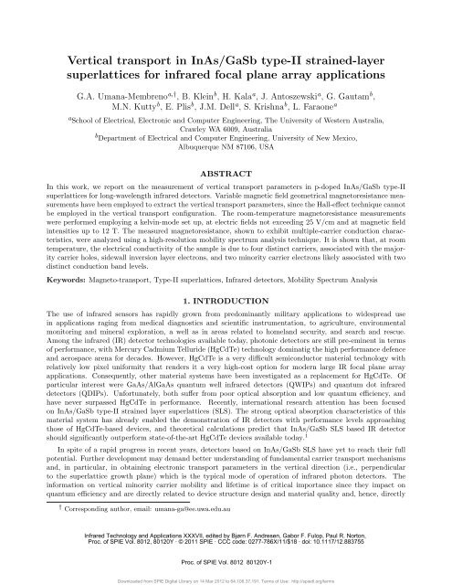
<strong>Vertical</strong> <strong>transport</strong> <strong>in</strong> <strong>InAs</strong>/<strong>GaSb</strong> <strong>type</strong>-<strong>II</strong> stra<strong>in</strong>ed-<strong>layer</strong><strong>superlattices</strong> <strong>for</strong> <strong>in</strong>frared focal plane array applicationsG.A. Umana-Membreno a,† , B. Kle<strong>in</strong> b , H. Kala a , J. Antoszewski a , G. Gautam b ,M.N. Kutty b , E. Plis b , J.M. Dell a , S. Krishna b , L. Faraone aa School of Electrical, Electronic and Computer Eng<strong>in</strong>eer<strong>in</strong>g, The University of Western Australia,Crawley WA 6009, Australiab Department of Electrical and Computer Eng<strong>in</strong>eer<strong>in</strong>g, University of New Mexico,Albuquerque NM 87106, USAABSTRACTIn this work, we report on the measurement of vertical <strong>transport</strong> parameters <strong>in</strong> p-doped <strong>InAs</strong>/<strong>GaSb</strong> <strong>type</strong>-<strong>II</strong><strong>superlattices</strong> <strong>for</strong> long-wavelength <strong>in</strong>frared detectors. Variable magnetic field geometrical magnetoresistance measurementshave been employed to extract the vertical <strong>transport</strong> parameters, s<strong>in</strong>ce the Hall-effect technique cannotbe employed <strong>in</strong> the vertical <strong>transport</strong> configuration. The room-temperature magnetoresistance measurementswere per<strong>for</strong>med employ<strong>in</strong>g a kelv<strong>in</strong>-mode set up, at electric fields not exceed<strong>in</strong>g 25 V/cm and at magnetic field<strong>in</strong>tensities up to 12 T. The measured magnetoresistance, shown to exhibit multiple-carrier conduction characteristics,were analyzed us<strong>in</strong>g a high-resolution mobility spectrum analysis technique. It is shown that, at roomtemperature, the electrical conductivity of the sample is due to four dist<strong>in</strong>ct carriers, associated with the majoritycarrier holes, sidewall <strong>in</strong>version <strong>layer</strong> electrons, and two m<strong>in</strong>ority carrier electrons likely associated with twodist<strong>in</strong>ct conduction band levels.Keywords: Magneto-<strong>transport</strong>, Type-<strong>II</strong> <strong>superlattices</strong>, Infrared detectors, Mobility Spectrum Analysis1. INTRODUCTIONThe use of <strong>in</strong>frared sensors has rapidly grown from predom<strong>in</strong>antly military applications to widespread use<strong>in</strong> applications rag<strong>in</strong>g from medical diagnostics and scientific <strong>in</strong>strumentation, to agriculture, environmentalmonitor<strong>in</strong>g and m<strong>in</strong>eral exploration, a well as <strong>in</strong> areas related to homeland security, and search and rescue.Among the <strong>in</strong>frared (IR) detector technologies available today, photonic detectors are still pre-em<strong>in</strong>ent <strong>in</strong> termsof per<strong>for</strong>mance, with Mercury Cadmium Telluride (HgCdTe) technology dom<strong>in</strong>atig the high per<strong>for</strong>mance defenceand aerospace arena <strong>for</strong> decades. However, HgCdTe is a very difficult semiconductor material technology withrelatively low pixel uni<strong>for</strong>mity that renders it a very high-cost option <strong>for</strong> modern large IR focal plane arrayapplications. Consequently, other material systems have been <strong>in</strong>vestigated as a replacement <strong>for</strong> HgCdTe. Ofparticular <strong>in</strong>terest were GaAs/AlGaAs quantum well <strong>in</strong>frared detectors (QWIPs) and quantum dot <strong>in</strong>frareddetectors (QDIPs). Un<strong>for</strong>tunately, both suffer from poor optical absorption and low quantum efficiency, andhave never surpassed HgCdTe <strong>in</strong> per<strong>for</strong>mance. Recently, <strong>in</strong>ternational research attention has been focusedon <strong>InAs</strong>/<strong>GaSb</strong> <strong>type</strong>-<strong>II</strong> stra<strong>in</strong>ed <strong>layer</strong> <strong>superlattices</strong> (SLS). The strong optical absorption characteristics of thismaterial system has already enabled the demonstration of IR detectors with per<strong>for</strong>mance levels approach<strong>in</strong>gthose of HgCdTe-based devices, and theoretical calculations predict that <strong>InAs</strong>/<strong>GaSb</strong> SLS based IR detectorshould significantly outper<strong>for</strong>m state-of-the-art HgCdTe devices available today. 1In spite of a rapid progress <strong>in</strong> recent years, detectors based on <strong>InAs</strong>/<strong>GaSb</strong> SLS have yet to reach their fullpotential. Further development may demand better understand<strong>in</strong>g of fundamental carrier <strong>transport</strong> mechanismsand, <strong>in</strong> particular, <strong>in</strong> obta<strong>in</strong><strong>in</strong>g electronic <strong>transport</strong> parameters <strong>in</strong> the vertical direction (i.e., perpendicularto the superlattice growth plane) which is the typical mode of operation of <strong>in</strong>frared photon detectors. The<strong>in</strong><strong>for</strong>mation on vertical m<strong>in</strong>ority carrier mobility and lifetime is of critical importance s<strong>in</strong>ce they impact onquantum efficiency and are directly related to device structure design and material quality and, hence, directly† Correspond<strong>in</strong>g author, email: umana-ga@ee.uwa.edu.auInfrared Technology and Applications XXXV<strong>II</strong>, edited by Bjørn F. Andresen, Gabor F. Fulop, Paul R. Norton,Proc. of SPIE Vol. 8012, 80120Y · © 2011 SPIE · CCC code: 0277-786X/11/$18 · doi: 10.1117/12.883755Proc. of SPIE Vol. 8012 80120Y-1Downloaded from SPIE Digital Library on 14 Mar 2012 to 64.106.37.191. Terms of Use: http://spiedl.org/terms
the majority carrier holes, sidewall <strong>in</strong>version <strong>layer</strong> electrons, and two m<strong>in</strong>ority carrier electrons likely associatedwith two dist<strong>in</strong>ct conduction band levels.ACKNOWLEDGMENTSThis work was supported by the Australian Research Council under the Discovery Project Grants Scheme(DP1096846).REFERENCES1. A. Rogalski, “New material systems <strong>for</strong> third generation <strong>in</strong>frared photodetectors,” Opto-Elect. Rev. 16,pp. 458–482, 2008.2. B. Kle<strong>in</strong>, E. Plis, M. N. Kutty, N. Gautam, A. Albrecht, S. Myers, and S. Krishna, “Varshni parameters <strong>for</strong><strong>InAs</strong>/<strong>GaSb</strong> stra<strong>in</strong>ed <strong>layer</strong> superlattice <strong>in</strong>frared photodetectors,” J. Phys. D 44(7), p. 075102, 2011.3. H. S. Kim, E. Plis, A. Khoshakhlagh, S. Myers, N. Gautam, Y. D. Sharma, L. R. Dawson, S. Krishna,S. J. Lee, and S. K. Noh, “Per<strong>for</strong>mance improvement of <strong>InAs</strong>/<strong>GaSb</strong> stra<strong>in</strong>ed <strong>layer</strong> superlattice detectors byreduc<strong>in</strong>g surface leakage currents with SU-8 passivation,” Appl. Phys. Lett. 96(3), p. 033502, 2010.4. M. C. Gold and D. A. Nelson, “Variable magnetic field Hall effect measurements and analyses of high purity,Hg vacancy (p-<strong>type</strong>) HgCdTe,” J. Vac. Sci. Technol. A 4(4), pp. 2040–2046, 1986.5. W. A. Beck and J. R. Anderson, “Determ<strong>in</strong>ation of electrical <strong>transport</strong> properties us<strong>in</strong>g a novel magneticfield-dependent Hall technique,” J. Appl. Phys. 62(2), pp. 541–554, 1987.6. Z. Dziuba and M. Gorska, “Analysis of the electrical-conduction uys<strong>in</strong>g an iterative method,” J. Phys.<strong>II</strong>I 2(7), pp. 99–110, 1992.7. J. Antoszewski, D. Seymeour, L. Faraone, J. R. Meyer, and C. A. Hoffman, “Magneto-<strong>transport</strong> characterizationus<strong>in</strong>g quantitative mobility-spectrum analysis,” J. Electron. Mat. 24(9), pp. 1255–1262, 1995.8. I. Vurgaftman, J. R. Meyer, C. A. Hoffman, D. Redfern, J. Antoszewski, L. Faraone, and J. R. L<strong>in</strong>demuth,“Improved quantitative mobility spectrum analysis <strong>for</strong> Hall characterization,” J. Appl. Phys. 84(9),pp. 4966–4973, 1998.9. S. Kiatgamolchai, M. Myronov, O. A. Mironov, V. G. Kantser, E. H. C. Parker, and T. E. Whall, “Mobilityspectrum computational analysis us<strong>in</strong>g a maximum entropy approach,” Phys. Rev. E 66(3), p. 036705, 2002.10. D. Chrast<strong>in</strong>a, J. P. Hague, and D. R. Leadley, “Application of Bryan’s algorithm to the mobility spectrumanalysis of semiconductor devices,” J. Appl. Phys. 94(10), pp. 6583–6590, 2003.11. J. Rothman, J. Meilhan, G. Perrais, J.-P. Belle, and O. Gravrand, “Maximum entropy mobility spectrumanalysis of HgCdTe heterostructures,” J. Electron. Mat. 35(6), pp. 1174–1184, 2006.12. G. Umana-Membreno, J. Antoszewski, L. Faraone, E. Smith, G. Venzor, S. Johnson, and V. Phillips, “Investigationof Multicarrier Transport <strong>in</strong> LPE-Grown Hg 1−x Cd x Te Layers,” J. Electron. Mat. 39, pp. 1023–1029,2010.Proc. of SPIE Vol. 8012 80120Y-6Downloaded from SPIE Digital Library on 14 Mar 2012 to 64.106.37.191. Terms of Use: http://spiedl.org/terms


