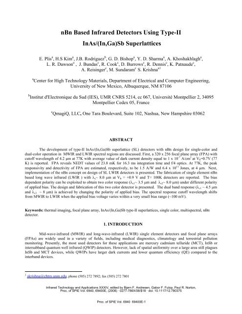
nBn based infrared detectors using type-II InAs/(In,Ga)Sb superlattices
nBn based infrared detectors using type-II InAs/(In,Ga)Sb superlattices
nBn based infrared detectors using type-II InAs/(In,Ga)Sb superlattices

You also want an ePaper? Increase the reach of your titles
YUMPU automatically turns print PDFs into web optimized ePapers that Google loves.
<strong>nBn</strong> Based <strong>In</strong>frared Detectors Using Type-<strong>II</strong><br />
<strong><strong>In</strong>As</strong>/(<strong>In</strong>,<strong>Ga</strong>)<strong>Sb</strong> Superlattices<br />
E. Plis a , H.S Kim a , J.B. Rodriguez b , G. D. Bishop a , Y. D. Sharma a , A. Khoshakhlagh a ,<br />
L. R. Dawson a , J. Bundas c , R. Cook c , D. Burrows c , R. Dennis c , K. Patnaude c ,<br />
A. Reisinger c , M. Sundaram c S. Krishna a1<br />
a Center for High Technology Materials, Department of Electrical and Computer Engineering,<br />
University of New Mexico, Albuquerque, NM 87106<br />
b <strong>In</strong>stitut d'Electronique du Sud (IES), UMR CNRS 5214, cc 067, Université Montpellier 2, 34095<br />
Montpellier Cedex 05, France<br />
c QmagiQ, LLC, One Tara Boulevard, Suite 102, Nashua, New Hampshire 03062<br />
ABSTRACT<br />
The development of <strong>type</strong>-<strong>II</strong> <strong><strong>In</strong>As</strong>/(<strong>In</strong>,<strong>Ga</strong>)<strong>Sb</strong> superlattice (SL) <strong>detectors</strong> with <strong>nBn</strong> design for single-color and<br />
dual-color operation in MWIR and LWIR spectral regions are discussed. First, a 320 x 256 focal plane array (FPA) with<br />
cutoff wavelength of 4.2 µm at 77K with average value of dark current density equal to 1 x 10 -7 A/cm 2 at V b =0.7V (77<br />
K) is reported. FPA reveals NEDT values of 23.8 mK for 16.3 ms integration time and f/4 optics. At 77K, the peak<br />
responsivity and detectivity of FPA are estimated, respectively, to be 1.5 A/W and 6.4 x 10 11 Jones, at 4 µm. Next,<br />
implementation of the <strong>nBn</strong> concept on design of SL LWIR <strong>detectors</strong> is presented. The fabrication of single element <strong>nBn</strong><br />
<strong>based</strong> long wave <strong>infrared</strong> (LWIR ) with λ c ~ 8.0 µm at V b = +0.9 V and T= 100K <strong>detectors</strong> are reported. The bias<br />
dependent polarity can be exploited to obtain two color response (λ c1 ~ 3.5 µm and λ c2 ~ 8.0 µm) under different polarity<br />
of applied bias. The design and fabrication of this two color detector is presented. The dual band response (λ c1 ~ 4.5 µm<br />
and λ c2 ~ 8 µm) is achieved by changing the polarity of applied bias. The spectral response cutoff wavelength shifts<br />
from MWIR to LWIR when the applied bias voltage varies within a very small bias range (~100 mV).<br />
Keywords: thermal imaging, focal plane array, <strong><strong>In</strong>As</strong>/(<strong>In</strong>,<strong>Ga</strong>)<strong>Sb</strong> <strong>type</strong>-<strong>II</strong> <strong>superlattices</strong>, single color, multispectral, <strong>nBn</strong><br />
detector.<br />
1. INTRODUCTION<br />
Mid-wave-<strong>infrared</strong> (MWIR) and long-wave-<strong>infrared</strong> (LWIR) single element <strong>detectors</strong> and focal plane arrays<br />
(FPAs) are widely used in a variety of fields, including medical diagnostics, climatology and terrestrial pollution<br />
monitoring. Presently, the most used <strong>detectors</strong> for these applications are mercury cadmium telluride (MCT), <strong>In</strong><strong>Sb</strong> or<br />
intersubband quantum well <strong>infrared</strong> (QWIP) <strong>detectors</strong>. However, lack of spatial uniformity over a large area still plagues<br />
<strong>In</strong><strong>Sb</strong> and MCT devices, while QWIPs have larger dark currents and lower quantum efficiency (QE) compared to the<br />
interband devices.<br />
1 skrishna@chtm.unm.edu, phone (505) 272 7892; fax (505) 272 7801<br />
<strong>In</strong>frared Technology and Applications XXXIV, edited by Bjørn F. Andresen, <strong>Ga</strong>bor F. Fulop, Paul R. Norton,<br />
Proc. of SPIE Vol. 6940, 69400E, (2008) · 0277-786X/08/$18 · doi: 10.1117/12.780375<br />
Proc. of SPIE Vol. 6940 69400E-1
Proposed by Smith and Mailhiot 1 in the 1980s, <strong>detectors</strong> <strong>based</strong> on <strong><strong>In</strong>As</strong>/<strong>Ga</strong><strong>Sb</strong> <strong>superlattices</strong> (SLs) have attracted<br />
a lot of attention over the past few years as a possible alternative to present-day IR detection systems. The <strong><strong>In</strong>As</strong>/<strong>Ga</strong><strong>Sb</strong><br />
SLs consist of alternating layers of nanoscale materials whose thicknesses vary from 4-20 nm. These heterostructures are<br />
characterized by a broken-gap <strong>type</strong>-<strong>II</strong> alignment as illustrated on the Figure 1. The overlap of electron (hole) wave<br />
functions between adjacent <strong><strong>In</strong>As</strong> (<strong>Ga</strong><strong>Sb</strong>) layers results in the formation of an electron (hole) minibands in the conduction<br />
(valence) band. Optical transitions between holes localized in <strong>Ga</strong><strong>Sb</strong> layers and electrons confined in <strong><strong>In</strong>As</strong> layers are<br />
employed for the detection of <strong>infrared</strong> radiation. The effective bandgap of the <strong><strong>In</strong>As</strong>/<strong>In</strong><strong>Ga</strong><strong>Sb</strong> SLs can be tailored from<br />
3µm to 30 µm by varying thickness of constituent layers, thus allowing fabrication of devices with operating<br />
wavelengths spanning the entire IR region<br />
The effective mass of the superlattice is not dependent on the bandgap, unlike the case of bulk semiconductor<br />
material. <strong>In</strong> contrast with QWIPs, normal incidence absorption is permitted in SLs, resulting in high quantum efficiency.<br />
The larger effective mass in SLs leads to a reduction of tunneling currents. Large splitting between heavy-hole and lighthole<br />
valence subbands due to strain in the SLs contributes to the suppression of Auger recombination. Commercial<br />
availability of low defect density substrates and a high degree of uniformity for <strong>II</strong>I-V processing over a large area also<br />
offers technological advantages for the SLs. This makes <strong>detectors</strong> <strong>based</strong> on SLs an attractive technology for the<br />
realization of high performance single element <strong>detectors</strong> and FPAs.<br />
Presently all SLs <strong>detectors</strong> are <strong>based</strong> on a photodiode (p-on-n or n-on-p) design. <strong>In</strong> this case, the optically active<br />
area of the photodiode is defined by an etched mesa as shown on the Figure 2 (a). During the mesa isolation process, the<br />
periodic nature of the idealized crystal structure ends abruptly at the mesa lateral surface. Disturbance of the periodic<br />
potential function due to a broken crystal lattice leads to allowed electronic quantum states within the energy band gap of<br />
SLs, resulting in large surface leakage currents. The suppression of these currents is the most demanding challenge for<br />
present day SLs technology, especially for LWIR and VLWIR spectral regions, since the dimensions of SLS pixels have<br />
to be scaled to ~ 20 µm in FPAs.<br />
<strong>In</strong> order to overcome the limitation imposed by surface leakage currents, a stable surface passivation layer is<br />
needed. So far, various approaches have been proposed such as the deposition of polyimide layer 2 , overgrowth of wide<br />
band gap material 3 , deposition of passivation sulphur coating electrochemically 4 and post etch treatment in chemical<br />
solutions 5 . However, these passivation methods are either sensitive to the cut-off wavelength of the device or complicates<br />
the fabrication process of <strong>detectors</strong> and FPAs.<br />
<strong><strong>In</strong>As</strong><br />
<strong><strong>In</strong>As</strong><br />
Electron<br />
miniband E<br />
Cl<br />
Hole —<br />
miniband<br />
Yl<br />
iHHn1n1r<br />
— I— I — I —<br />
__________________<br />
$1<br />
I I<br />
Absorption<br />
<strong>Ga</strong><strong>Sb</strong><br />
Figure 1. Schematic bandgap alignment of Type <strong>II</strong> <strong><strong>In</strong>As</strong>/<strong>Ga</strong><strong>Sb</strong> <strong>superlattices</strong> (SLs).<br />
Recently 6 , a new heterostructure design with extremely low surface currents has been proposed. This socalled<br />
<strong>nBn</strong> structure consists of a n-<strong>type</strong> narrow band-gap contact and absorber layers separated by a 50-100 nm thick<br />
wide band-gap barrier layer. A 100K increase in the background limited <strong>infrared</strong> photodetector (BLIP) temperature has<br />
been demonstrated. Implementation of the <strong>nBn</strong> design for <strong><strong>In</strong>As</strong>/<strong>Ga</strong><strong>Sb</strong> MWIR SLs single element <strong>detectors</strong> has been<br />
reported 7,8 . Unlike a conventional photodiode processing, the size of the device with <strong>nBn</strong> design is not defined by the<br />
Proc. of SPIE Vol. 6940 69400E-2
etch dimensions but, rather by the lateral diffusion length of minority carriers (holes), as illustrated in Figure 2(b).<br />
SLs-<strong>based</strong> <strong>detectors</strong> with <strong>nBn</strong> design and special processing scheme showed a dark current reduction of two orders of<br />
magnitude (at 77K) in comparison with conventional photodiode processing and values of quantum efficiency and<br />
shot-noise-limited specific detectivity comparable to the state-of-the-art p-i-n diodes <strong>based</strong> on the SLs. However, no<br />
FPAs <strong>based</strong> on <strong><strong>In</strong>As</strong>/<strong>Ga</strong><strong>Sb</strong> SLs <strong>detectors</strong> with <strong>nBn</strong> design have been reported yet.<br />
<strong>In</strong> the present work we report on our efforts to fabricate FPAs <strong>based</strong> on <strong><strong>In</strong>As</strong>/<strong>Ga</strong><strong>Sb</strong> SL <strong>nBn</strong>-design <strong>detectors</strong><br />
for the MWIR spectral region. Also, we extend the <strong>nBn</strong>-design concept <strong>using</strong> <strong><strong>In</strong>As</strong>/<strong>In</strong><strong>Ga</strong><strong>Sb</strong> SLs in order to achieve<br />
LWIR detection.<br />
Metallization<br />
Metallization<br />
P-Contact<br />
N-Contact<br />
Barrier<br />
J surface<br />
Absorber<br />
DL<br />
DL<br />
J bulk<br />
N-Contact<br />
Substrate<br />
Absorber<br />
(a)<br />
(b)<br />
Figure 2. Schematic of (a) conventionally defined mesa (b) shallow etched isolation <strong>nBn</strong> device. <strong>In</strong> the latter case<br />
active area is defined by the by diffusion length (DL) of the minority carriers (holes)<br />
2. NBN <strong><strong>In</strong>As</strong>/<strong>Ga</strong><strong>Sb</strong> SLS MWIR FPA IMAGERS<br />
N-Contact<br />
Substrate<br />
Substrate<br />
The devices presented in this work were grown on Te-doped epi-ready (100) <strong>Ga</strong><strong>Sb</strong> substrates <strong>using</strong> a solid<br />
source molecular beam epitaxy VG-80 system. The system was equipped with SUMO ® cells for gallium and indium, a<br />
standard effusion cell for aluminum and cracker cells for antimony and arsenic. Growth rates were calibrated by<br />
monitoring the intensity oscillations in the reflected high-energy electron diffraction (RHEED) patterns and confirmed<br />
by growth of calibration SL samples with different thickness of SL period. More details about the growth procedure can<br />
be found elsewhere 9 . Growths were performed on 2” diameter unintentionally doped epi-ready n-<strong>type</strong> <strong>Ga</strong><strong>Sb</strong> (001)<br />
substrates. The detector structure consists of a 100 nm thick Al 0.2 <strong>Ga</strong> 0.8 <strong>Sb</strong> etch stop layer followed by a 360 nm bottom<br />
contact layer formed by 8 monolayers (MLs) <strong><strong>In</strong>As</strong>:Si (n = 4 x 10 18 cm -3 )/8 MLs <strong>Ga</strong><strong>Sb</strong> SLS. Then a 2.4 µm thick nonintentionally<br />
doped (n.i.d.) absorber formed by 8 MLs <strong><strong>In</strong>As</strong>/ 8 MLs <strong>Ga</strong><strong>Sb</strong> SLS was grown followed by a 100nm thick<br />
Al 0.2 <strong>Ga</strong><strong>Sb</strong> barrier layer. The structure was terminated by a 100 nm n-<strong>type</strong> (n = 4 x 10 18 cm -3 ) top contact layer with the<br />
same composition as the bottom contact layer. The heterostructure schematic is shown in Figure 3.<br />
J bulk<br />
Proc. of SPIE Vol. 6940 69400E-3
SL (n) 100 nm<br />
Contact<br />
Al 0.2 <strong>Ga</strong><strong>Sb</strong> 100 nm<br />
Barrier<br />
SL nid 2.4 µm<br />
Absorber<br />
SL (n) 360 nm<br />
Contact<br />
Al 0.2 <strong>Ga</strong><strong>Sb</strong> 100 nm<br />
Etch stop layer<br />
<strong>Ga</strong><strong>Sb</strong>:Te 2”<br />
Substrate<br />
Figure 3. Heterostructure schematic of <strong><strong>In</strong>As</strong>/<strong>Ga</strong><strong>Sb</strong> SLs MWIR detector<br />
Each processed FPA die consists of 320 x 256 pixels with a 30 µm pitch. Processing was initiated by defining<br />
24 µm x 24 µm squares with standard UV photolithography and a shallow wet chemical etch <strong>using</strong> phosphoric acid was<br />
performed. It is to be noted that the depth of the shallow etch was equal to 0.15 nm, which corresponds to the middle of<br />
the barrier layer. Thus the active absorber layer underneath is untouched. Then an inductively coupled plasma (ICP) dry<br />
etch to the middle of the bottom contact layer on the three outermost rows and columns of the FPA was undertaken. A<br />
scanning electron microscope (SEM) image of a part of a fully processed FPA is shown in Figure 4 and illustrates the<br />
two steps of the etching process. Top and bottom contacts were then deposited <strong>using</strong> an electron beam metal evaporation<br />
system. We used Ti\Pt\Au (500Å\500Å\3000Å) as contact metals for both top and bottom ohmic contact metallization.<br />
Finally, to enable well defined <strong>In</strong>dium bumps, an under bump metal (UBM) deposition was conducted <strong>using</strong> Ti\Ni\Au<br />
(300Å\1500Å\500Å). <strong>In</strong>dium bumps with a thickness ~3 µm were thermally evaporated on the UBM metal pads.<br />
Following this, the FPAs were hybridized to ISC0209 read-out integrated circuits (ROICs) made by <strong>In</strong>digo.<br />
To reduce the free carrier absorption in the substrate and to minimize the thermal stress between the FPA and<br />
the ROIC under cool-down conditions, the backside of the FPAs were thinned by a combination of mechanical polishing<br />
and wet chemical etching. Hybridization and characterization of the FPAs were undertaken at QmagiQ, LLC. Hybrid<br />
FPAs were tested with a CamIRa <strong>infrared</strong> FPA evaluation system made by SE-IR Corp. with a Ge window for the<br />
imaging performance tests. For the tests, the background was a 300K scene under f/4 illumination. The applied bias was<br />
equal to 0.7V and is defined as a positive voltage applied to the bottom contact of the FPA.<br />
The noise equivalent temperature difference (NETD) was measured by acquiring a sequence of 25 image scans<br />
with the focal plane exposed to a uniform blackbody target at 30°C and extracting the temporal noise for each pixel. A<br />
histogram of the NETD distribution is shown in Figure 5 (a) for an integration time of 16.3 ms. Good spatial uniformity<br />
is obtained over the array, resulting in a median NETD value of 23.8 mK with a standard deviation of 10 mK at a FPA<br />
temperature of 77K. Pixel operability was equal to 79% with predominant single pixel faults without large clusters.<br />
Pixel outages probably originated from the weak connection between the ROIC and FPA since the thickness of indium<br />
bumps was equal only 3 µm and no reflow process was utilized.<br />
Proc. of SPIE Vol. 6940 69400E-4
fln 1 na<br />
Efl 1 fl<br />
smai<br />
nna I<br />
nwrinn<br />
winfln nfl<br />
a<br />
ncnn<br />
r ri Etn<br />
30µ<br />
m<br />
Figure 4. Scanning Electron Microscopy (SEM) image showing part of fully processed FPA with deposited indium<br />
bumps. The two-step etch process is illustrated.<br />
The measured average dark current density is presented in Figure 5(b). Extrapolated to an operating<br />
temperature of 77K, the average dark current density was as low as 1 x 10 -7 A/cm 2 (V b =0.7V). This value is comparable<br />
to the state-of-the-art reports for MWIR <strong>detectors</strong> <strong>based</strong> on a conventional photodiode design with a suitable passivation<br />
scheme.<br />
The external quantum efficiency (QE) was obtained <strong>using</strong> the spectral response curve from the test diode on the<br />
FPA chip with 380µm x 380µm optical area. Spectral measurements were performed <strong>using</strong> a Fourier Transform <strong>In</strong>frared<br />
Spectrometer (FTIR). Under 0.7V bias and at 77K the FPA exhibits a QE as high as 52% at 3.8 µm (Fig. 6). Peak<br />
responsivity and detectivity of FPA were estimated, respectively, to be 1.6 A/W and 6.7 x 10 11 Jones, at 3.8 µm and 77K<br />
(V b =0.7V). Values of specific detectivity, QE and responsivity as a function of wavelength are presented in Figure 7.<br />
The responsivity was calculated assuming no photoconductive gain.<br />
ZOS1SVINfl - mea juaiin Apsua<br />
6000.<br />
5000.<br />
Mean vaIue23.8mK<br />
3<br />
yTT TTT TT<br />
u000<br />
3000.<br />
a)<br />
E<br />
2000.<br />
z<br />
1000.<br />
0.<br />
iL25 50 75 100<br />
a<br />
a<br />
a<br />
C<br />
a<br />
L09<br />
9L<br />
09<br />
T V<br />
99<br />
YVY<br />
TV<br />
VT<br />
06<br />
ainwiadwaj. j)<br />
96<br />
OO<br />
9O<br />
NEdT(mK)<br />
Figure 5. (a) Histogram of the noise equivalent temperature difference (NETD) distribution in the FPA for an<br />
integration time of 16.3 ms with f/4 optics (b) Average dark current density of FPA.<br />
A thermal image taken with 320 x 256 MWIR FPA camera <strong>based</strong> on <strong><strong>In</strong>As</strong>/<strong>Ga</strong><strong>Sb</strong> SL at a detector temperature of<br />
77 K and integration time of 16.3 ms is shown in Figure 7. A two point non-uniformity correction (NUC) was used for<br />
the imaging. Temperatures of 20°C and 40°C were utilized as the low and high temperature for the NUC correction<br />
Proc. of SPIE Vol. 6940 69400E-5
algorithm. The bright areas of the image represent warmer regions whereas the dark areas exhibit colder regions. <strong>In</strong> the<br />
figure, the facial imprint of the fingerprints after touching the cold can are clearly visible, demonstrating the good<br />
imaging quality of thermal imager.<br />
1.6<br />
1.6<br />
Responsivity, D*<br />
Quantum efficiency<br />
T = 77K<br />
V b<br />
= 0.7V<br />
7x10 11<br />
6x10 11<br />
Quantum efficiency<br />
1.2<br />
0.8<br />
Responsivity (A/W)<br />
1.2<br />
0.8<br />
0.4 0.4<br />
5x10 11<br />
4x10 11<br />
3x10 11<br />
2x10 11<br />
1x10 11<br />
D* (Jones)<br />
0.0<br />
0.0<br />
1 2 3 4 5 6<br />
Wavelength (µm)<br />
0<br />
Figure 6. Spectral detectivity D*, responsivity and quantum efficiency for 4.2 µm cut-off wavelength FPA<br />
Figure 7. Thermal image taken with 320x256 <strong><strong>In</strong>As</strong>/<strong>Ga</strong><strong>Sb</strong> SLs <strong>nBn</strong> camera at a detector temperature of 77 K and<br />
integration time of 16.3 ms. A two-point non-uniformity correction was utilized.<br />
3. NBN <strong><strong>In</strong>As</strong>/<strong>Ga</strong><strong>Sb</strong> SLS LWIR SINGLE-ELEMENT DETECTORS<br />
The structure of the <strong>nBn</strong> <strong><strong>In</strong>As</strong>/<strong>Ga</strong><strong>Sb</strong> SLs LWIR detector is similar to that described in the previous section except for<br />
the composition of the absorber SL. The structure consists of a 100 nm thick Al 0.2 <strong>Ga</strong> 0.8 <strong>Sb</strong> etch stop layer followed by a<br />
480 nm bottom contact layer formed by 8 MLs <strong><strong>In</strong>As</strong>:<strong>Ga</strong>Te (n = 4 x 10 18 cm -3 )/8 MLs <strong>Ga</strong><strong>Sb</strong>:<strong>Ga</strong>Te SLS. Then a 1.9 µm<br />
thick non-intentionally doped (n.i.d.) absorber formed by 9 MLs <strong><strong>In</strong>As</strong>/ 5 MLs <strong>Ga</strong><strong>In</strong> 0.25 <strong>Sb</strong> SLS was grown, followed by a<br />
100nm thick Al 0.2 <strong>Ga</strong><strong>Sb</strong> barrier layer. A 100 nm n-<strong>type</strong> top contact layer with the same composition and doping level as<br />
the bottom contact layer capped the structure. The heterostructure schematic of the LWIR <strong>nBn</strong> detector is presented in<br />
Figure 8 (a) .<br />
Proc. of SPIE Vol. 6940 69400E-6
SL (n) 100 nm<br />
MWIR Contact<br />
Al 0.2 <strong>Ga</strong><strong>Sb</strong> 100 nm<br />
Barrier<br />
SL nid 2.4 µm<br />
LWIR Absorber<br />
SL (n) 480 nm<br />
MWIR Contact<br />
Counts/s<br />
SL 0<br />
SL LWIR<br />
10 4 0<br />
<strong>Ga</strong><strong>Sb</strong><br />
(004)<br />
SL MWIR<br />
10 4 10<br />
<strong>Ga</strong><strong>Sb</strong><br />
+1<br />
3<br />
-1<br />
10 2<br />
-2<br />
10 3<br />
Ω/2θ ( ο )<br />
-3<br />
+2<br />
10 2<br />
-4<br />
+3<br />
10 1<br />
+4<br />
Counts/s<br />
30.6 30.9 31.2<br />
0<br />
Al 0.2 <strong>Ga</strong><strong>Sb</strong> 100 nm<br />
Etch stop layer<br />
<strong>Ga</strong><strong>Sb</strong>:Te 2”<br />
Substrate<br />
10 0<br />
26 28 30 32 34 36<br />
Ω/2θ ( ο )<br />
(a)<br />
(b)<br />
Figure 8. (a) The heterostructure schematic and (b) (004) XRD scan of LWIR SLs detector<br />
Symmetric (004) X-ray scan was performed on the sample with a Philips double-crystal X-ray diffractometer<br />
<strong>using</strong> the Cu-K α1 line and is presented in Figure 8 (b). Peaks from both SLs forming the contacts (MWIR) and absorbing<br />
layer (LWIR) are visible. The LWIR superlattice is slightly compressively strained, with a lattice mismatch to the <strong>Ga</strong><strong>Sb</strong><br />
substrate equal to 0.2%. The full width at half maximum (FWHM) of the 1 st satellite peak of LWIR SL is equal to 32<br />
arcsec, thus indicating the good crystalline quality of the material. The overall periodicity of the structure, measured by<br />
the fringe spacing of the superlattice peaks, is found to be 39.2 Å and 48.4 Å for the LWIR and MWIR SLs, respectively.<br />
These values are in a good agreement with the nominal ones.<br />
Normalized spectral response (a.u.)<br />
1.0<br />
0.8<br />
0.6<br />
0.4<br />
0.2<br />
x 50<br />
V b<br />
= -0.7 volts<br />
V b<br />
= 0.9 volts<br />
0.0<br />
1 2 3 4 5 6 7 8 9 10 11<br />
Wavelength (µm)<br />
100 K<br />
150 K<br />
Top<br />
contact<br />
Top contact<br />
Barrier<br />
(b)<br />
Barrier<br />
LWIR<br />
absorber<br />
LWIR<br />
absorber<br />
(a)<br />
(c)<br />
Figure 9. (a) Normalized spectral response of <strong>nBn</strong> LWIR detector at different temperatures under different polarities<br />
of applied bias; Schematic band diagram for the <strong>nBn</strong> LWIR detector under (b) forward and (c) reverse bias<br />
Proc. of SPIE Vol. 6940 69400E-7
Normal incidence single pixel photodiodes were fabricated <strong>using</strong> standard lithography with apertures ranging<br />
from 25-300 µm in diameter. Processing was initiated with the formation of ohmic contacts on the n-<strong>type</strong> top contact<br />
layer followed by dry etching of the device to the top of the barrier (etch depth 100 nm) for the mesa definition. Then the<br />
wafer was patterned with the photoresist, and a deep dry etch (etch depth ~2 µm) to the middle of the bottom n-<strong>type</strong><br />
contact layer was performed. Finally, an ohmic contact was evaporated on the bottom contact layer. Ti (500 Å) / Pt (500<br />
Å) /Au (3000 Å) was used as n-contact metal for both top and bottom contacts. Devices were then wire bonded to a<br />
leadless chip carrier for further characterization.<br />
Spectral measurements were performed <strong>using</strong> a FTIR spectrometer and a Keithley 428 preamplifier. Figure 9<br />
shows the normalized spectral response (obtained by dividing the photocurrent of the SLS detector with that obtained<br />
<strong>using</strong> a pyroelectric detector) for a 300 µm diameter device for two different temperatures at the different polarities of<br />
applied bias. For the <strong>nBn</strong> detector structure, forward bias is defined as a negative voltage applied to the top contact of<br />
the detector. As depicted in Figure 9, the <strong>nBn</strong> LWIR detector structure demonstrated two color response (λ c1 ~ 3.5 µm<br />
and λ c2 ~ 8.0 µm) under different polarity of applied bias.<br />
Schematic band diagrams for the <strong>nBn</strong> LWIR detector under forward (negative voltage on the top) and reverse<br />
(positive voltage on the top) biases are shown in Figure 9(b) and Figure 9(c), respectively. Under forward bias, the photo<br />
carriers are collected from the absorber. When the device is under reverse bias, the photo carriers from the heavily doped<br />
(n-<strong>type</strong>) contact layer are collected, while those from the absorber are blocked by the barrier. Heavily doped <strong><strong>In</strong>As</strong> in the<br />
top contact layer results in a larger optical bandgap due to the Moss-Burstein effect and is the source of the MWIR<br />
signal. Thus, the two color response come from the detector absorber (LWIR signal) and top contact layer (MWIR<br />
signal).<br />
4. NBN INAS/GASB SLS DUAL COLOR (MWIR/LWIR) DETECTORS<br />
On the basis of the results obtained from the MWIR and LWIR <strong>nBn</strong> <strong>detectors</strong>, we designed a two color <strong>nBn</strong><br />
structure 10 . The heterostructure schematic of such structure is presented in Figure 10 (a). The growth procedure started<br />
with the deposition of a 480 nm bottom contact layer formed by 8 ML <strong><strong>In</strong>As</strong>:<strong>Ga</strong>Te (n=4 x 10 18 cm −3 )/8 ML <strong>Ga</strong><strong>Sb</strong> SLS.<br />
Then a 1.8 µm thick LWIR absorber consisting of unintentionally doped 9 ML <strong><strong>In</strong>As</strong>/5 ML <strong>In</strong> 0.25 <strong>Ga</strong> 0.75 <strong>Sb</strong> SLS was grown<br />
followed by a 1.5 µm thick MWIR absorber composed of 8 ML <strong><strong>In</strong>As</strong>/8 ML <strong>Ga</strong><strong>Sb</strong> SLS. The thicknesses of the LWIR and<br />
MWIR absorbers were designed to be approximately the same. A 100 nm Al0.2<strong>Ga</strong>0.8<strong>Sb</strong> barrier separated the two<br />
absorbers. The structure was capped with a ~ 0.1 µm top contact layer with the same composition and doping level as the<br />
bottom contact layer.<br />
SL (n) 97 nm<br />
MWIR Contact<br />
SL nid 1.5 µm<br />
MWIR Absorber<br />
Al 0.2 <strong>Ga</strong><strong>Sb</strong> 100 nm<br />
Barrier<br />
SL nid 1.8 µm<br />
LWIR Absorber<br />
SL (n) 480 nm<br />
MWIR Contact<br />
<strong>Ga</strong><strong>Sb</strong>:Te 2”<br />
Substrate<br />
Counts/s<br />
<strong>Ga</strong><strong>Sb</strong><br />
10 4 SLMWIR SL LWIR<br />
0<br />
0<br />
+1 LWIR<br />
10 3<br />
10 2<br />
10 1<br />
+1 MWIR<br />
-1 LWIR<br />
-2 LWIR -1 MWIR<br />
-2 MWIR +2 MWIR<br />
+2 LWIR<br />
Al<strong>Ga</strong><strong>Sb</strong> Barrier<br />
10 0<br />
27 28 29 30 31 32 33 34<br />
Ω/2θ ( ο )<br />
(a)<br />
(b)<br />
Figure 10. (a) The heterostructure schematic and (b) (004) XRD scan of multispectral (LWIR/MWIR) <strong>nBn</strong> SLs<br />
detector<br />
Proc. of SPIE Vol. 6940 69400E-8
Symmetric (004) X-ray scan was performed on the multispectral <strong>nBn</strong> SLs sample and is presented in Figure 8<br />
(b). The lattice mismatch of LWIR and MWIR SLs to the <strong>Ga</strong><strong>Sb</strong> substrate is 0.13% (compressive strain) and –0.04%<br />
(tensile strain), respectively. The full width at half maximum (FWHM) of the 1 st satellite peak of the LWIR SL is equal<br />
to 25 arcsec (45 arcsec for the MWIR SLs). The periods of LWIR and MWIR SLs were measured from the fringe<br />
spacing of the SLs peaks and were found to be 42.2 Å and 48.2 Å for the LWIR and MWIR SLs, respectively.<br />
The detector material was processed to operate at normal incidence as single pixel photodiodes with apertures<br />
ranging from 25 to 300 µm. The processing procedure was similar to that described earlier for <strong>nBn</strong> LWIR single element<br />
<strong>detectors</strong> in Section 2.<br />
The relative spectral responses of the bicolor structure are shown in Fig. 11 (a). The data clearly show cutoff<br />
wavelengths λ c1 ~ 4.5 µm and λ c2 ~ 8 µm under different polarities of applied bias. When a forward bias is applied, the<br />
carriers from the LW absorber are collected, and when a reverse bias is applied, the carriers from the MW absorber are<br />
collected. It is to be noted that there will be barriers between unintentionally doped LWIR layer and the bottom n-contact<br />
that can impede the transport.<br />
An interesting feature in the detector’s responsivity vs. wavelength behavior was noticed while the spectral<br />
response of the multispectral <strong>nBn</strong> detector within the range of applied bias from 0 to + 0.1V was being investigated<br />
(Figure 11 (b)). The data clearly indicate that the response cutoff wavelength shifts from MWIR to LWIR when the<br />
applied bias voltage varies between 0 and +0.1 V. As the applied bias voltage increases from 0 to +0.1 V, the intensity of<br />
the MWIR response decreases whereas the intensity of LWIR response increases. Due to this bias dependent feature of<br />
the spectral response, a single detector can be operated at multiple biases sequentially, whereby the detector’s spectral<br />
response changes in accordance with the applied bias. Consequently, one of the advantages of <strong>nBn</strong> design is that it does<br />
not require multiple contacts per pixel, which reduces the cost and complexity associated with the fabrication process.<br />
Normalized spectral response (a.u.)<br />
1.0<br />
0.8<br />
0.6<br />
0.4<br />
0.2<br />
0.0<br />
V b<br />
= + 0.5 V<br />
V b<br />
= -0.6 V<br />
3 4 5 6 7 8 9 10<br />
Wavelength (µm)<br />
100 K<br />
150 K<br />
Spectral response (a.u)<br />
0.06<br />
0.05<br />
0.04<br />
0.03<br />
0.02<br />
0.01<br />
0.00<br />
2 3 4 5 6 7 8 9 10<br />
Wavelength(µm)<br />
0 V<br />
+ 0.01 V<br />
+ 0.05 V<br />
+ 0.09 V<br />
+ 0.1 V<br />
Figure 11. (a) Normalized spectral response of the multispectral <strong>nBn</strong> detector at different temperatures and different<br />
polarity of applied bias (b) Spectral response of the multispectral <strong>nBn</strong> detector within a range of applied bias from 0 to<br />
+0.1V<br />
5. SUMMARY AND CONCLUSION<br />
The development of <strong>nBn</strong> <strong>based</strong> <strong>detectors</strong> for MWIR and LWIR spectral regions <strong>using</strong> <strong>type</strong>-<strong>II</strong> <strong><strong>In</strong>As</strong>/(<strong>In</strong>,<strong>Ga</strong>)<strong>Sb</strong><br />
SL has been presented. First, we demonstrated a 320 x 256 FPA with cutoff wavelength of 4.2 µm at 77K. The average<br />
value of the dark current density (1 x 10 -7 A/cm 2 at 77K (V b =0.7V) proved comparable to that reported for the state-ofthe-art<br />
MWIR SLs photodiodes utilizing some passivation schemes. At 77K, FPA reveals an average NEDT of 23.8 mK<br />
Proc. of SPIE Vol. 6940 69400E-9
for 16.3 ms integration time. The peak responsivity and detectivity of FPA were estimated to be 1.6 A/W and 6.7 x 10 11<br />
Jones, respectively, at 3.8 µm and 77K.<br />
We then described our implementation of the <strong>nBn</strong> concept to design SL LWIR <strong>detectors</strong>. Within addition to the<br />
expected long-wave cut off wavelength, the <strong>nBn</strong> LWIR detector structure demonstrated two color response (λ c1 ~ 3.5 µm<br />
and λ c2 ~ 8.0 µm) under different polarity of applied bias.<br />
Finally, a multispectral <strong>nBn</strong> detector structure has been presented. The dual band response (λ c1 ~ 4.5 µm and<br />
λ c2 ~ 8 µm) was achieved by changing the polarity of applied bias. The spectral response shows a significant change in<br />
the LWIR to MWIR ratio within a very small bias range (100 mV), making it compatible with commercially available<br />
readout integrated circuits.<br />
6. ACKNOWLEDGEMENT<br />
Support from AFRL Grant FA9453-07-C-0171 and HOT MWIR program is acknowledged.<br />
1. D.L. Smith and C. Mailhiot, J. Appl. Phys., 62, 2545 (1987).<br />
2. A. Hood, P.-Y. Delaunay, D. Hoffman, B.-M. Nguyen, Y. Wei and M. Razeghi, Appl. Phys. Lett. 90, 233513 (2007).<br />
3. R. Rehm, M. Walther, F. Fuchs, J. Schmitz and J. Fleissner, Appl. Phys. Lett., 86,173501 (2005).<br />
4. E. Plis, J.B. Rodriguez, S.J. Lee and S. Krishna, Electron. Lett., 42, 1248 (2006).<br />
5. A. Gin, Y. Wei, A. Hood, A. Bajowala, V. Yazdanpanah and M. Razeghi, Appl. Phys. Lett., 84, 2037 (2004).<br />
6 . Maimon and G. W. Wicks, Appl. Phys. Lett. 89, 151109 (2006).<br />
7 J.B. Rodriguez, E. Plis, G. Bishop, Y.D. Sharma, H. Kim, L.R. Dawson and S. Krishna, Appl. Phys. Lett. 91, 043514<br />
(2007).<br />
8 G. Bishop, E. Plis, J.B. Rodriguez, Y. D. Sharma, H.S. Kim, L. R. Dawson, and S. Krishna, J. Vac. Sci. Technol., B 26<br />
(3), 1 (2008)<br />
9. E. Plis, S. Annamalai, K. T. Posani, S. Krishna, R. A. Rupani, and S. Ghosh, J. Appl. Phys., 100, 014510 (2006).<br />
10. A. Khoshakhlagh, J. B. Rodriguez, E. Plis, G. D. Bishop, Y. D. Sharma, H. S. Kim, L. R. Dawson, and S. Krishna,<br />
Appl. Phys. Lett. 91, 263504 (2007).<br />
Proc. of SPIE Vol. 6940 69400E-10