nBn based infrared detectors using type-II InAs/(In,Ga)Sb superlattices
nBn based infrared detectors using type-II InAs/(In,Ga)Sb superlattices
nBn based infrared detectors using type-II InAs/(In,Ga)Sb superlattices

Create successful ePaper yourself
Turn your PDF publications into a flip-book with our unique Google optimized e-Paper software.
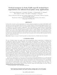
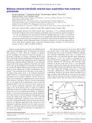
Proposed by Smith and Mailhiot 1 in the 1980s, <strong>detectors</strong> <strong>based</strong> on <strong><strong>In</strong>As</strong>/<strong>Ga</strong><strong>Sb</strong> <strong>superlattices</strong> (SLs) have attracted<br />
a lot of attention over the past few years as a possible alternative to present-day IR detection systems. The <strong><strong>In</strong>As</strong>/<strong>Ga</strong><strong>Sb</strong><br />
SLs consist of alternating layers of nanoscale materials whose thicknesses vary from 4-20 nm. These heterostructures are<br />
characterized by a broken-gap <strong>type</strong>-<strong>II</strong> alignment as illustrated on the Figure 1. The overlap of electron (hole) wave<br />
functions between adjacent <strong><strong>In</strong>As</strong> (<strong>Ga</strong><strong>Sb</strong>) layers results in the formation of an electron (hole) minibands in the conduction<br />
(valence) band. Optical transitions between holes localized in <strong>Ga</strong><strong>Sb</strong> layers and electrons confined in <strong><strong>In</strong>As</strong> layers are<br />
employed for the detection of <strong>infrared</strong> radiation. The effective bandgap of the <strong><strong>In</strong>As</strong>/<strong>In</strong><strong>Ga</strong><strong>Sb</strong> SLs can be tailored from<br />
3µm to 30 µm by varying thickness of constituent layers, thus allowing fabrication of devices with operating<br />
wavelengths spanning the entire IR region<br />
The effective mass of the superlattice is not dependent on the bandgap, unlike the case of bulk semiconductor<br />
material. <strong>In</strong> contrast with QWIPs, normal incidence absorption is permitted in SLs, resulting in high quantum efficiency.<br />
The larger effective mass in SLs leads to a reduction of tunneling currents. Large splitting between heavy-hole and lighthole<br />
valence subbands due to strain in the SLs contributes to the suppression of Auger recombination. Commercial<br />
availability of low defect density substrates and a high degree of uniformity for <strong>II</strong>I-V processing over a large area also<br />
offers technological advantages for the SLs. This makes <strong>detectors</strong> <strong>based</strong> on SLs an attractive technology for the<br />
realization of high performance single element <strong>detectors</strong> and FPAs.<br />
Presently all SLs <strong>detectors</strong> are <strong>based</strong> on a photodiode (p-on-n or n-on-p) design. <strong>In</strong> this case, the optically active<br />
area of the photodiode is defined by an etched mesa as shown on the Figure 2 (a). During the mesa isolation process, the<br />
periodic nature of the idealized crystal structure ends abruptly at the mesa lateral surface. Disturbance of the periodic<br />
potential function due to a broken crystal lattice leads to allowed electronic quantum states within the energy band gap of<br />
SLs, resulting in large surface leakage currents. The suppression of these currents is the most demanding challenge for<br />
present day SLs technology, especially for LWIR and VLWIR spectral regions, since the dimensions of SLS pixels have<br />
to be scaled to ~ 20 µm in FPAs.<br />
<strong>In</strong> order to overcome the limitation imposed by surface leakage currents, a stable surface passivation layer is<br />
needed. So far, various approaches have been proposed such as the deposition of polyimide layer 2 , overgrowth of wide<br />
band gap material 3 , deposition of passivation sulphur coating electrochemically 4 and post etch treatment in chemical<br />
solutions 5 . However, these passivation methods are either sensitive to the cut-off wavelength of the device or complicates<br />
the fabrication process of <strong>detectors</strong> and FPAs.<br />
<strong><strong>In</strong>As</strong><br />
<strong><strong>In</strong>As</strong><br />
Electron<br />
miniband E<br />
Cl<br />
Hole —<br />
miniband<br />
Yl<br />
iHHn1n1r<br />
— I— I — I —<br />
__________________<br />
$1<br />
I I<br />
Absorption<br />
<strong>Ga</strong><strong>Sb</strong><br />
Figure 1. Schematic bandgap alignment of Type <strong>II</strong> <strong><strong>In</strong>As</strong>/<strong>Ga</strong><strong>Sb</strong> <strong>superlattices</strong> (SLs).<br />
Recently 6 , a new heterostructure design with extremely low surface currents has been proposed. This socalled<br />
<strong>nBn</strong> structure consists of a n-<strong>type</strong> narrow band-gap contact and absorber layers separated by a 50-100 nm thick<br />
wide band-gap barrier layer. A 100K increase in the background limited <strong>infrared</strong> photodetector (BLIP) temperature has<br />
been demonstrated. Implementation of the <strong>nBn</strong> design for <strong><strong>In</strong>As</strong>/<strong>Ga</strong><strong>Sb</strong> MWIR SLs single element <strong>detectors</strong> has been<br />
reported 7,8 . Unlike a conventional photodiode processing, the size of the device with <strong>nBn</strong> design is not defined by the<br />
Proc. of SPIE Vol. 6940 69400E-2