nBn based infrared detectors using type-II InAs/(In,Ga)Sb superlattices
nBn based infrared detectors using type-II InAs/(In,Ga)Sb superlattices
nBn based infrared detectors using type-II InAs/(In,Ga)Sb superlattices

You also want an ePaper? Increase the reach of your titles
YUMPU automatically turns print PDFs into web optimized ePapers that Google loves.
Normal incidence single pixel photodiodes were fabricated <strong>using</strong> standard lithography with apertures ranging<br />
from 25-300 µm in diameter. Processing was initiated with the formation of ohmic contacts on the n-<strong>type</strong> top contact<br />
layer followed by dry etching of the device to the top of the barrier (etch depth 100 nm) for the mesa definition. Then the<br />
wafer was patterned with the photoresist, and a deep dry etch (etch depth ~2 µm) to the middle of the bottom n-<strong>type</strong><br />
contact layer was performed. Finally, an ohmic contact was evaporated on the bottom contact layer. Ti (500 Å) / Pt (500<br />
Å) /Au (3000 Å) was used as n-contact metal for both top and bottom contacts. Devices were then wire bonded to a<br />
leadless chip carrier for further characterization.<br />
Spectral measurements were performed <strong>using</strong> a FTIR spectrometer and a Keithley 428 preamplifier. Figure 9<br />
shows the normalized spectral response (obtained by dividing the photocurrent of the SLS detector with that obtained<br />
<strong>using</strong> a pyroelectric detector) for a 300 µm diameter device for two different temperatures at the different polarities of<br />
applied bias. For the <strong>nBn</strong> detector structure, forward bias is defined as a negative voltage applied to the top contact of<br />
the detector. As depicted in Figure 9, the <strong>nBn</strong> LWIR detector structure demonstrated two color response (λ c1 ~ 3.5 µm<br />
and λ c2 ~ 8.0 µm) under different polarity of applied bias.<br />
Schematic band diagrams for the <strong>nBn</strong> LWIR detector under forward (negative voltage on the top) and reverse<br />
(positive voltage on the top) biases are shown in Figure 9(b) and Figure 9(c), respectively. Under forward bias, the photo<br />
carriers are collected from the absorber. When the device is under reverse bias, the photo carriers from the heavily doped<br />
(n-<strong>type</strong>) contact layer are collected, while those from the absorber are blocked by the barrier. Heavily doped <strong><strong>In</strong>As</strong> in the<br />
top contact layer results in a larger optical bandgap due to the Moss-Burstein effect and is the source of the MWIR<br />
signal. Thus, the two color response come from the detector absorber (LWIR signal) and top contact layer (MWIR<br />
signal).<br />
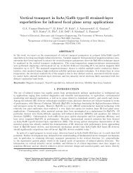
4. NBN INAS/GASB SLS DUAL COLOR (MWIR/LWIR) DETECTORS<br />
On the basis of the results obtained from the MWIR and LWIR <strong>nBn</strong> <strong>detectors</strong>, we designed a two color <strong>nBn</strong><br />
structure 10 . The heterostructure schematic of such structure is presented in Figure 10 (a). The growth procedure started<br />
with the deposition of a 480 nm bottom contact layer formed by 8 ML <strong><strong>In</strong>As</strong>:<strong>Ga</strong>Te (n=4 x 10 18 cm −3 )/8 ML <strong>Ga</strong><strong>Sb</strong> SLS.<br />
Then a 1.8 µm thick LWIR absorber consisting of unintentionally doped 9 ML <strong><strong>In</strong>As</strong>/5 ML <strong>In</strong> 0.25 <strong>Ga</strong> 0.75 <strong>Sb</strong> SLS was grown<br />
followed by a 1.5 µm thick MWIR absorber composed of 8 ML <strong><strong>In</strong>As</strong>/8 ML <strong>Ga</strong><strong>Sb</strong> SLS. The thicknesses of the LWIR and<br />
MWIR absorbers were designed to be approximately the same. A 100 nm Al0.2<strong>Ga</strong>0.8<strong>Sb</strong> barrier separated the two<br />
absorbers. The structure was capped with a ~ 0.1 µm top contact layer with the same composition and doping level as the<br />
bottom contact layer.<br />
SL (n) 97 nm<br />
MWIR Contact<br />
SL nid 1.5 µm<br />
MWIR Absorber<br />
Al 0.2 <strong>Ga</strong><strong>Sb</strong> 100 nm<br />
Barrier<br />
SL nid 1.8 µm<br />
LWIR Absorber<br />
SL (n) 480 nm<br />
MWIR Contact<br />
<strong>Ga</strong><strong>Sb</strong>:Te 2”<br />
Substrate<br />
Counts/s<br />
<strong>Ga</strong><strong>Sb</strong><br />
10 4 SLMWIR SL LWIR<br />
0<br />
0<br />
+1 LWIR<br />
10 3<br />
10 2<br />
10 1<br />
+1 MWIR<br />
-1 LWIR<br />
-2 LWIR -1 MWIR<br />
-2 MWIR +2 MWIR<br />
+2 LWIR<br />
Al<strong>Ga</strong><strong>Sb</strong> Barrier<br />
10 0<br />
27 28 29 30 31 32 33 34<br />
Ω/2θ ( ο )<br />
(a)<br />
(b)<br />
Figure 10. (a) The heterostructure schematic and (b) (004) XRD scan of multispectral (LWIR/MWIR) <strong>nBn</strong> SLs<br />
detector<br />
Proc. of SPIE Vol. 6940 69400E-8