Mid Infrared Focal Plane Arrays with Nanoscale Quantum Dots and ...
Mid Infrared Focal Plane Arrays with Nanoscale Quantum Dots and ...
Mid Infrared Focal Plane Arrays with Nanoscale Quantum Dots and ...
You also want an ePaper? Increase the reach of your titles
YUMPU automatically turns print PDFs into web optimized ePapers that Google loves.
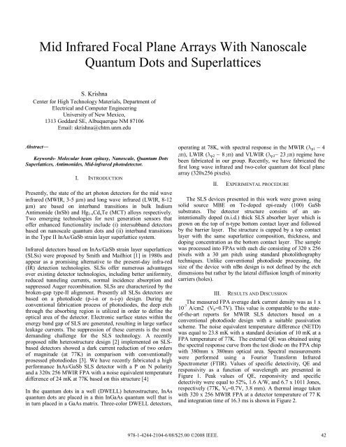
<strong>Mid</strong> <strong>Infrared</strong> <strong>Focal</strong> <strong>Plane</strong> <strong>Arrays</strong> With <strong>Nanoscale</strong><strong>Quantum</strong> <strong>Dots</strong> <strong>and</strong> SuperlatticesS. KrishnaCenter for High Technology Materials, Department ofElectrical <strong>and</strong> Computer EngineeringUniversity of New Mexico,1313 Goddard SE, Albuquerque NM 87106Email: skrishna@chtm.unm.eduif desiredAbstract—Keywords- Molecular beam epitaxy, <strong>Nanoscale</strong>, <strong>Quantum</strong> <strong>Dots</strong>Superlattices, Antimonides, <strong>Mid</strong>-infrared photodetector.I. INTRODUCTIONPresently, the state of the art photon detectors for the mid waveinfrared (MWIR, 3-5 µm) <strong>and</strong> long wave infrared (LWIR, 8-12µm) are based on interb<strong>and</strong> transitions in bulk IndiumAntimonide (InSb) <strong>and</strong> Hg 1-x Cd x Te (MCT) alloys respectively.Two emerging technologies for next generation sensors thatoffer enhanced functionality include (i) intersubb<strong>and</strong> detectorsbased on nanoscale quantum dots <strong>and</strong> (ii) interb<strong>and</strong> transitionsin the Type II InAs/GaSb strain layer superlattice system.<strong>Infrared</strong> detectors based on InAs/GaSb strain layer superlattices(SLSs) were proposed by Smith <strong>and</strong> Mailhiot [1] in 1980s <strong>and</strong>appear as a promising alternative to the present-day infra-red(IR) detection technologies. SLSs offer numerous advantagesover existing detector technologies, including better uniformity,reduced tunneling currents, normal incidence absorption <strong>and</strong>suppressed Auger recombination. SLSs are characterized by thebroken-gap type-II alignment. Presently all SLSs detectors arebased on a photodiode (p-i-n or n-i-p) design. During theconventional fabrication process of photodiodes, the deep etchthrough the absorbing region is utilized in order to define theoptical area of the detector. Electronic surface states <strong>with</strong>in theenergy b<strong>and</strong> gap of SLS are generated, resulting in large surfaceleakage currents. The suppression of these currents is the mostdem<strong>and</strong>ing challenge for the SLS technology. A recentlyproposed nBn heterostructure design [2] implemented on SLSbaseddetectors showed a dark current reduction of two ordersof magnitude (at 77K) in comparison <strong>with</strong> conventionallyprosessed photodiodes [3]. We have recently fabricated a highperformance InAs/GaSb SLS detector <strong>with</strong> a P on N polarity<strong>and</strong> a 320x 256 MWIR FPA <strong>with</strong> a noise equivalent temperaturedifference of 24 mK at 77K based on this structure [4}In the quantum dots in a well (DWELL) heterostructure, InAsquantum dots are placed in a thin InGaAs quantum well that isin turn placed in a GaAs matrix. Three-color DWELL detectors,operating at 78K, <strong>with</strong> spectral response in the MWIR ( p1 ~ 4), LWIR ( p2 ~ 8 ) <strong>and</strong> VLWIR ( p3 ~ 23 ) regime havebeen fabricated in our group. Recently, we have fabricated thefirst long wave infrared <strong>and</strong> two-color quantum dot focal planearray (320x256 pixels).II.EXPERIMENTAL PROCEDUREThe SLS devices presented in this work were grown usingsolid source MBE on Te-doped epi-ready (100) GaSbsubstrates. The detector structure consists of an unintentionallydoped (n.i.d.) thick SLS absorber layer which isgrown on the top of n-type bottom contact layer <strong>and</strong> followedby the barrier layer. The structure is capped by a top contactlayer <strong>with</strong> the same superlattice composition, thickness, <strong>and</strong>doping concentration as the bottom contact layer. The samplewas processed into FPAs <strong>with</strong> each die consisting of 320 x 256pixels <strong>with</strong> a 30 m pitch using st<strong>and</strong>ard photolithographytechniques. Unlike conventional photodiode processing, thesize of the device <strong>with</strong> nBn design is not defined by the etchdimensions but rather by the lateral diffusion length of minoritycarriers (holes).III. RESULTS AND DISCUSSIONThe measured FPA average dark current density was as 1 x10 -7 A/cm2 (V b =0.7V). This value is comparable to the stateof-the-artreports for MWIR SLS detectors based on aconventional photodiode design <strong>with</strong> a suitable passivationscheme. The noise equivalent temperature difference (NETD)was equal to 23.8 mK <strong>with</strong> a st<strong>and</strong>ard deviation of 10 mK at aFPA temperature of 77K. The external QE was obtained usingthe spectral response curve from the test diode on the FPA chip<strong>with</strong> 380mm x 380mm optical area. Spectral measurementswere performed using a Fourier Transform <strong>Infrared</strong>Spectrometer (FTIR). Values of specific detectivity, QE <strong>and</strong>responsivity as a function of wavelength are presented inFigure 1. Peak values of QE, responsivity <strong>and</strong> specificdetectivity were equal to 52%, 1.6 A/W, <strong>and</strong> 6.7 x 10¹¹ Jones,respectively (77K, V b =0.7V, 3.8 mm). A thermal image taken<strong>with</strong> 320 x 256 MWIR FPA at a detector temperature of 77 K<strong>and</strong> integration time of 16.3 ms is shown in Figure 2.978-1-4244-2104-6/08/$25.00 ©2008 IEEE. 42
Figure 3. Images taken <strong>with</strong> a long wave infrared quantum dots in a wellfocal plane array (320x256).Figure 1. Spectral detectivity D*, responsivity <strong>and</strong> quantum efficiency for4.2 µm cut-off wavelength FPAACKNOWLEDGMENTWork supported by NSF, AFRL, AFOSR <strong>and</strong> DARPA.REFERENCESFigure 2. Thermal image taken <strong>with</strong> a MWIR 320x256 InAs/GaSb SLs nBncamera at a detector temperature of 77 K <strong>and</strong> integration time of 16.3 ms.<strong>Focal</strong> plane arrays were also made using nanoscalequantum dots using a similar procedure. Imaging obtainedfrom these arrays in the long wave infrared region are shown inFig. 3.[1] D.L. Smith <strong>and</strong> C. Mailhiot, J. Appl. Phys., vol. 62, 2545-2549 (1987).[2] S. Maimon <strong>and</strong> G. W. Wicks, Appl. Phys. Lett., vol. 89, 151109-15111(2006)[3] J.B. Rodriguez, E. Plis, G. Bishop, Y.D. Sharma, H. Kim, L.R. Dawson<strong>and</strong> S. Krishna, Appl. Phys. Lett., vol. 91, 043514-043516 (2007).[4] H. S. Kim, E. Plis, J. B. Rodriguez, G. D. Bishop, Y. D. Sharma, L. R.Dawson, S. Krishna, J. Bundas, R. Cook, D. Burrows, R. Dennis, K.Patnaude, A. Reisinger, <strong>and</strong> M. Sundaram, Appl. Phys. Lett. 92, 183502(2008)43


