Packaging Nano Wafer Level - National University of Singapore
Packaging Nano Wafer Level - National University of Singapore
Packaging Nano Wafer Level - National University of Singapore

You also want an ePaper? Increase the reach of your titles
YUMPU automatically turns print PDFs into web optimized ePapers that Google loves.
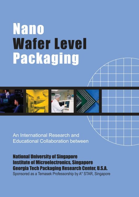
<strong>Nano</strong><strong>Wafer</strong> <strong>Level</strong><strong>Packaging</strong>"<strong>Nano</strong> Chips Need <strong>Nano</strong> <strong>Packaging</strong>"Pr<strong>of</strong>. Rao R. TummalaTemasek Pr<strong>of</strong>essor, NUS, <strong>Singapore</strong>Director, <strong>Packaging</strong> Research Center,Georgia Tech, USAAn International Collaborationin Research and Education<strong>National</strong> <strong>University</strong> <strong>of</strong> <strong>Singapore</strong>Institute <strong>of</strong> Microelectronics, <strong>Singapore</strong>Georgia Institute <strong>of</strong> Technology, USAPr<strong>of</strong>. Andrew TayNUS, Program ManagerDr. Mahadevan K. IyerIME, Program ManagerResearch Area Georgia Tech NUS IMEElectrical Design M. Swaminathan Simon Ang Mahadevan K. IyerMaterials &ProcessesC.P. WongAshok SaxenaSuresh SitaramanE.T. KangK.G. NeohManoj GuptaAndrew TaySimon AngY.C. LiangV. KripeshWong Ee HuaCelaine WongMarvin LoTest & Burn-inDavid KeezerSimon AngW.K. WongMihai RotaruReliabilitySuresh SitaramanAndrew TayC.T. LimK.M. LimW.K. WongWong Ee Hua100 Micron BoardVenky SundaramV. KripeshMarvin LoIntegrated TestbedDavid KeezerM. SwaminathanVenky SundaramC.P. WongAndrew TaySimon AngET KangW.K. WongMahadevan K. IyerV. KripeshWong Ee HuaMihai RotaruResearch Staff &Students2 Post DoctoralAssociates12 GraduateStudents3 Post Doctoral Fellows, 2 ResearchEngineers, 16 Graduate Students,5 Research Staff
JOBS & THE ECONOMYHEALTH & WELLNESSIncreasing economic opportunities to those who need themmost is a foundation <strong>of</strong> sustainability. While still much too high,the unemployment rate has decreased in Wards 4, 5, 7, and 8,and new businesses are opening their doors across the District.Partners throughout the city are working to make our economystronger and more sustainable.OUR PROGRESS• The new Office <strong>of</strong> the Deputy Mayor for Greater EconomicOpportunity will create more opportunities to the middleclass for residents seeking employment or starting andgrowing new small businesses.• The Department <strong>of</strong> Consumer and Regulatory Affairs launchedthe Small Business Resource Center to streamline permittingand provide technical assistance for new businesses.• 162 small businesses were certified as certified businessenterprises by the Department <strong>of</strong> Small and Local BusinessDevelopment since April 2014.• Think Local First and the Council <strong>of</strong> the District <strong>of</strong>Columbia have named 2015 the “Year <strong>of</strong> Local” to strengthensmall businesses, identify emerging markets, and highlightlocal entrepreneurs.• The Deputy Mayor for Planning and Economic Developmentlaunched OurRFP, which will put community priorities frontand center in new economic development proposals.• $9.50 per hour is the new minimum wage, which willincrease to $10.50 per hour on July 1, 2015, one <strong>of</strong> thehighest rates in the country.While health disparities between wards remain a challenge,District Government, community organizations, and localbusinesses are working together to increase access to qualityhealthcare, make healthy food more available, and create safeplaces to be active outside.OUR PROGRESS• 92% <strong>of</strong> District residents are covered under health insuranceplans thanks in part to DC Health Link connecting familiesand small businesses to quality new health insurance plans.• The Student Food Ambassador Program was established toprovide direct communication between DC Public Schoolsand students about school meals, and 40% <strong>of</strong> the total DCPSfood service budget was spent on locally produced food.• 21 local healthcare facilities signed the Sustainable DCHealthcare Sector Sustainability Pledge to green theiroperations and better engage the community on sustainabilityand health issues.• 820 residents benefited from 73 free cooking classes inWards 5, 7, and 8 thanks to DC Central Kitchen and theDistrict Department <strong>of</strong> Health, and 6,415 low-income residentsreceived fresh produce at farmers markets and healthycorner stores through the Freggie Bucks Program.• The Department <strong>of</strong> Health and Department <strong>of</strong> Parks andRecreation are launching Fit DC, a nutrition and physicalfitness citywide health and wellness campaign for residents.2014 Unemploymentby WardWARD 1: 5.4% (2012: 5.9%)WARD 2: 4.8% (2012: 3%)WARD 3: 4.6% (2012: 3.3%)WARD 4: 6.9% (2012: 9.4%)WARD 5: 9.3% (2012: 13.4%)WARD 6: 6.2% (2012: 6.5%)WARD 7: 13% (2012: 16.9%)WARD 8: 16.3% (2012: 19.9%)16PLAYGROUNDSBUILT OR RENOVATED3 Second Year Progress Report
Electrical DesignObjectives: Maintaining signal integrity represents one <strong>of</strong> the major bottlenecksfor enabling reliable systems. This is due to the increase in speed, reduction involtage, increase in power, and the integration <strong>of</strong> mixed signal functions in futuresystems. Examples <strong>of</strong> such systems include electro-optic USB interfaces,wireless devices, server farms and computing applications. Due to the fasttransition <strong>of</strong> digital signals, the analog behavior <strong>of</strong> these signals becomes veryimportant. Issues such as cross talk, reflections, switching noise, eye patternsand delay, therefore, have to be addressed for the design <strong>of</strong> systems. <strong>Wafer</strong> levelpackaging <strong>of</strong> circuits provides a very attractive solution for future micro-systems,especially in the mobile computing area. This is because <strong>of</strong> reduced parasiticsand smaller form factor.Approach: The combination <strong>of</strong> wafer level packaging and a high-density printedcircuit board with embedded functionality has many advantages for the design <strong>of</strong>mixed signal <strong>Nano</strong> systems. The wafer level package reduces parasitics throughshort compliant or rigid leads, improves isolation by separating incompatiblecircuitry and enables much better matching <strong>of</strong> components for developingintegrated solutions. Both modeling and experimental techniques will bepursued. In particular, the following electrical issues will be studied in detail: 1)design <strong>of</strong> the chip-to-package compliant or rigid leads and transitions forsupporting digital and RF signals 20-50GHz; 2) design <strong>of</strong> the chip-to-packagecompliant and rigid leads to supply >200W <strong>of</strong> power to the chips with minimumpower supply noise and electro-migration problems and; 3) study <strong>of</strong> transmissionline and radiation effects <strong>of</strong> the chip-to-package compliant or rigid leads forsupporting 20-50GHz digital signals.Research Focus:Design <strong>of</strong> the transitions from the chip into the high-density printed circuitboard through the compliant or rigid leads. Modeling tools and measurementtechniques will be used for the design <strong>of</strong> these transitions.3Design <strong>of</strong> the compliant or rigid leads with minimum inductance that cansupport fast transient currents for supporting multi-gigahertz digital circuitsdissipating > 200W <strong>of</strong> power. Power distribution analysis tools developed atGeorgia Tech will be enhanced to model the geometries. These will becorrelated with measurements on custom chips.Modeling <strong>of</strong> the current density through the compliant or rigid leads toestimate high frequency current densities and their effect on electromigration.Radiation and transmission line measurements to better understand theelectromagnetic behavior <strong>of</strong> the leads at frequencies 20-50GHz.
Design, Modeling and ReliabilityModeling, Assessment & EvaluationStructuralAnalysisReliabilityTestVehicleMechanicalTest andEvaluationObjectives: With the continued reduction in IC feature size and with theincreased demand for better performance and lower cost, there is a need for aninnovative, yet reliable, interconnect technology. According to the NTRSroadmap in the U.S., the interconnect pitch, will be less than 50 microns, and inselect opto-electronic applications, it can be as small as 10 microns. Most <strong>of</strong> theexisting interconnect technologies today, even with dramatic improvements, areincapable <strong>of</strong> addressing this ultra-fine pitch requirement. Therefore, there is acompelling need to understand theModel Designsfor Reliabilitythermo-mechanical designrequirements, failure mechanisms andreliability <strong>of</strong> such interconnects anddevelop suitable interconnects startingwith design for reliability.4Materials CharacterizationReliability Modeling & VerificationGeneral Interconnection Design and Optimization SchemeTestDesignsVerifyDesignApproach: To cater to the CTEmismatch between the die and thesubstrate, two basic designs <strong>of</strong> ultra-finepitch interconnections have beenproposed: compliant and rigid. Acompliant interconnection reduces thestress but tends to yield lower electricalperformance and mechanical flimsinesscompared to rigid interconnections. On the other hand, rigid interconnectionshave to sustain higher stresses resulting in likely failures by fracture or fatigue.However, this deficiency may be overcome by the use <strong>of</strong> high-strength <strong>Nano</strong>structuredmaterials. The mechanical, thermal and electrical characteristics <strong>of</strong>various interconnection designs falling under the two main categories will bestudied extensively through modeling and simulation and a few likely-to-succeeddesigns will be identified. Specimens <strong>of</strong> the short-listed designs will then befabricated and the material properties and processes characterized. Constitutivemodels <strong>of</strong> new materials will be obtained. The state <strong>of</strong> stress in theinterconnections will be modeled for the entire fabrication process in order topredict more precisely the reliability <strong>of</strong> the final product. Extensive reliability testswill also be conducted in order to study the failure mechanisms operating. Models<strong>of</strong> these failure mechanisms will be developed and used to predict the reliability<strong>of</strong> the final product. With such models developed, the design <strong>of</strong> theinterconnections can be further optimized through simulation and experimentalverification.Research Focus:Design:- Propose potential solutions for 100 micron and 20 micron pitches;- Critical evaluation <strong>of</strong> characteristics and challenges <strong>of</strong> each solution.Modeling:- Develop methodology for modeling material properties and processes;- Develop comprehensive models to predict failure mechanisms operating;- Develop integrated modeling methodology and design for reliability <strong>of</strong>WLP;- Explore the use <strong>of</strong> molecular dynamics and multi-scale modeling inreliability prediction <strong>of</strong> WLP.Materials Characterization:- Conduct experiments to characterize the properties <strong>of</strong> materials including<strong>Nano</strong>-structured materials;- Develop constitutive models <strong>of</strong> relevant materials.Failure Analysis and Reliability Tests:- Design and conduct reliability tests to study the operative failuremechanisms;- Develop failure analysis techniques and methodology to characterize thefailure mechanisms;- Demonstrate reliability <strong>of</strong> testbed.
<strong>Wafer</strong> <strong>Level</strong> Interconnect ApproachesObjectives: The overall objective is to develop fine pitch and low costinterconnect technologies for high-density wafer level packaging. The currentwafer level packages are at a pitch <strong>of</strong> 300-400 microns, serving primarily memoryproducts. The proposed pitch will explore different wafer level interconnecttechnologies for 20 micron and demonstrate 100 micron pitch meeting theelectrical, thermal and mechanical requirements.Approach: With the need <strong>of</strong> 20 to 100 micron pitch, both rigid and compliantinterconnect structures will be pursued in this thrust area. A total <strong>of</strong> 6 differentwafer level interconnect schemes are proposed:a) 100 micron pitch- Bed <strong>of</strong> nails (compliant)- Streched solder column (rigid)- Lead-free solder balls with no flow underfill (rigid)b) 20 micron pitch- <strong>Nano</strong>structured interconnect based on polymer-metal or metal-metalinterfacial composites (rigid)- <strong>Nano</strong> links- MEMs-fabricated interconnects (compliant)The wafer level packages with 100 micron pitch will be assembled into the finalintegrated test bed. The wafer level packages with 20 micron pitch incorporates<strong>Nano</strong> interconnects and will be studied form a research point <strong>of</strong> view.Research Focus:Explore and demonstrate promising materials and processes for 20 micronand 100 micron pitch wafer level interconnect schemes;5Select or develop metal and lead-free solder alloys and develop newcharacterization methodologies;Develop the processes involved in fabricating the interconnections;Optimize various processes for 100 micron scheme.100 Micron Pitch: 20 Micron Pitch:Silicon ChipSilicon ChipHigh Density BoardVery High Density BoardBed <strong>of</strong>NailsStretchedSolderColumnSolder Ballswith No FlowUnderfill<strong>Nano</strong>LinksMEMSInterconnect<strong>Nano</strong>Interconnect<strong>Wafer</strong> <strong>Level</strong> Interconnect Scheme
Potential <strong>of</strong> <strong>Nano</strong>-Structured MaterialsObjectives: The most aggressive wafer level packaging proposed is on 20micron pitch. At this pitch, the conventional solder ball technology does notguarantee the reliability <strong>of</strong> the IC-to-board joint. Compliant connection is onesolution but it may be expensive and it may not provide the best electricalproperties. Underfill around the solder is another solution but it makes theprocess complex and makes the technology expensive too. <strong>Nano</strong>interconnection is proposed because <strong>of</strong> its potential unique mechanical andelectrical properties.Approach: Experimental studies have demonstrated that there is considerablepotential for enhancing strength <strong>of</strong> materials through interface strengthening(increasing grain boundary area and/or phase boundary area) in several materialsystems such as Cu, Ni, Ni-base alloys and intermetallics, aluminum alloys, gold,and carbon steels. Mechanical strengthening in crystalline materials occurs as aresult <strong>of</strong> obstacles encountered by dislocations restricting their mobility.Obstacles to dislocation motion are in the form <strong>of</strong> (a) lack <strong>of</strong> appropriate number<strong>of</strong> primary slip systems (b) coherent and incoherent precipitates (c) interphaseand antiphase boundaries and (d) grain boundaries. Thus, reducingmicrostructural features to the <strong>Nano</strong>meter scale and creating more suchobstacles in the process, provides avenues for tailoring strength, toughness, andcreep properties, in addition to influencing electrical resistivity and solid-statediffusivity and solubility.Research Focus:6Identify promising <strong>Nano</strong>-stuctured materials systems for use in 20 micronpitch interconnects and produce them in experimental quantities forevaluation. The range <strong>of</strong> materials to be considered include monolithicmetals and alloys as well as composites containing <strong>Nano</strong>-structured metalsand alloys as particulate reinforcements and conductive polymers as matrix;Characterize the materials to obtain tensile strength, hardness, fracturetoughness and fatigue properties, and electrical properties, using noveltechniques such as <strong>Nano</strong> indentation, in-situ AFM/STEM, SEM. Developnew characterization techniques as needed;Develop modeling and simulation tools to extract most information fromtests and to aid in developing in-depth understanding <strong>of</strong> phenomena at the<strong>Nano</strong> level for its fullest exploitation in wafer level interconnect applications.Intercept grain diameter, nm10 4 10 3 10 2 10Vickers Microhardness, kg/mm 2800600400200Nickel Electroplate0 100 200 300Reciprocal square root <strong>of</strong> grain size, nm 2Microhardness <strong>of</strong> electroplated nickel as a function <strong>of</strong> reciprocal<strong>of</strong> the square root <strong>of</strong> grain size (Neiman, Weertman, and Siegel, 1991)
Test and Burn-In SystemObjectives: <strong>Wafer</strong> level packaging is incomplete without guaranteeing KnownGood Die (KGD). In conventional IC packaging it is done by test and burn in afterthe IC is packaged as QFP, BGA or CSP. But this individual test and burn-in atthe IC level is a sequential and expensive process. The objective <strong>of</strong> this task is todevelop strategies and implement them at 100 micron pitch at wafer level.Approach: The need to make electrical contacts to the interconnectingstructures with pitches <strong>of</strong> 20-100 microns presents tremendous challenges.Furthermore, the bandwidth requirements present tremendous challenges to theselection <strong>of</strong> materials as well as integration and fabrication methods. Presently,testing <strong>of</strong> wafer-level packaged devices is performed using fine-pitch probesdirectly on the wafer. It is expected that this approach will not be applicable tothe <strong>Nano</strong> wafer level.Test WorkStationMeasurementInstrumentTest Signal ProcessorInterposerD.U.T.<strong>Wafer</strong>Probing CardAn interposer, with a self-aligned, z-axis compliant and good electrical contactfeatures, will be designed and fabricated to serve as the electrical andmechanical interface between the N-WLP and the tester. Due to the largenumber <strong>of</strong> inputs/outputs on this N-WLP (in the order <strong>of</strong> 10,000 to 200,000 I/Osper cm 2 , it is anticipated that this interposer will not be able to handle therequired re-distribution task. As such, a test support processor (TSP) boardconsisting <strong>of</strong> a field-programmable array device, memory devices, sample-andholddevices, clocks, multiplexers, and others, will be integrated onto the top layer<strong>of</strong> the interposer, using the flip chip attachment method. The test signalprocessor will act as the tester with the required test stimuli and memory tocapture the tested data. In this way, only a few I/Os from the TSP are required foreach wafer level-packaged device.A burn-in system that simultaneously connects devices on several N-WLP ICswill also be developed. As in most burn-in requirements, the task <strong>of</strong> redistributingthe vast number <strong>of</strong> I/Os may not be the limiting factor as only specificelectrical connections are required during burn-in. An interposer, similar to theinterposer developed for wafer-level test, will be developed to serve as theelectrical and mechanical interface for burn-in.<strong>Wafer</strong> D.U.T.7Research Focus: Besides fabrication challenges, the other major challengeswill be the selection <strong>of</strong> materials and integration methods to meet the largebandwidth requirements <strong>of</strong> the interposer.Design and fabrication <strong>of</strong> the interposerDesign and fabrication <strong>of</strong> the test signal processorIntegration <strong>of</strong> the test signal processor onto the interposer to form theTSP interposerTest and characterization <strong>of</strong> the TSP interposerDesign and fabrication <strong>of</strong> a burn-in interposerIntegration <strong>of</strong> the burn-in interposer into a burn-in systemOptimization <strong>of</strong> test and burn-in strategy for NWLP
Integrated <strong>Wafer</strong> <strong>Level</strong> Test BedObjectives: The objective is to design and assemble an integrated test bed todemonstrate 100 micron pitch reliable wafer level packaged system. The test bedshall integrate all the above wafer level packaging technologies including the testand burn-in to mee the required mechanical and electrical integrity.Approach: The approach would be to integrate all the enabling technologies intoa testbed. The proposed specification for 100 micron pitch wafer level packageswill be designed into the testbed. The challenges from electrical signal integrityand thermo-mechanical reliability would be addressed in the 100 micron pitchtestbed design and development. The testbed is also intended to demonstrate thewafer level packaging materials and processes. The electrical testing will be donein two phases: 1) DC testing, demonstrating the technologies; and 2) functionaltesting, demonstrating the test features and compatibility <strong>of</strong> the technology totesting.Proposed Target Specification <strong>of</strong> the <strong>Nano</strong> <strong>Wafer</strong> <strong>Level</strong> PackagesSpecification: Present: Proposed:Specification: State <strong>of</strong> the Art Today: Proposed: 100 Micron Proposed: 20 MIcron100 micron 20 micronAcceptable Cost U.S. $50 to $150 0.5X 0.1XElectrical Digital and RF Digital and RF Digital and RF2-3 GHz 10 GHz 20-50 GHzThermomechanical JEDEC <strong>Level</strong> 3 JEDEC <strong>Level</strong> 2ReliabilityBoard <strong>Level</strong> Reliability8Die Size 7mm (0.8 sq. cm) 20 mm (4 sq. cm) 20 mm (4 sq. cm)Pitch 50 µm 100 µm 20 µmDistance from Neutral Point 10,000Interconnect Size 300 µm 30 µm 6-8 µmApplications Memories, Passives, RF-Ids Handheld Computing High Performance ComputingManufacturability Batch Processing Batch Processing Batch ProcessingEnbabling Technology RDL, UBM Comliant, Rigid <strong>Nano</strong> InterconnectTest and Burn-inMaterials Characterization,Processes,Test and Burn-inResearch Focus:Develop electrical design and simulation methodologies <strong>of</strong>the test bed to accommodate 100 micron pitch wafer levelpackages. The design and characterization techniques usedat the wafer level interconnects would be extended to thesystem test bed keeping in mind the 20-50GHz bandwidthgoal;Exploration and assessment <strong>of</strong> the thermo-mechanicalreliability.DC level testing and burn-in integrated into the board. Thetest strategies developed at the wafer level would beextended to board level testing;Design and development <strong>of</strong> 100 micron board demonstratingthe compatibility between the 100 micron pitch wafer and the100 micron board.
Enquiries and Contacts:Pr<strong>of</strong>essor Andrew Tay, Department <strong>of</strong> Mechanical Engineering,<strong>National</strong> <strong>University</strong> <strong>of</strong> <strong>Singapore</strong>, 9 Engineering Drive 1, <strong>Singapore</strong> 117576.Email: mpetayao@nus.edu.sgCarl Rust, Associate Director, <strong>Packaging</strong> Research CenterGeorgia Institute <strong>of</strong> Technology, 813 Ferst Drive, Room 351, Atlanta GA 30332 U.S.A.Email: crust@ee.gatech.eduDr. Mahadevan K. Iyer, R&D Manager, Advanced <strong>Packaging</strong> Development SupportInstitute <strong>of</strong> Microelectronics, 11 Science Park Road <strong>Singapore</strong> Science Park II <strong>Singapore</strong> 117685Email: iyer@ime.org.sgWebsites <strong>of</strong> Collaborating Institutions:<strong>National</strong> <strong>University</strong> <strong>of</strong> <strong>Singapore</strong>:http://www.nus.edu.sgInstitute <strong>of</strong> Microelectronics, <strong>Singapore</strong>:http://www.ime.org.sg<strong>Packaging</strong> Research Center, Georgia Tech, USA: http://www.prc.gatech.edu