Packaging Nano Wafer Level - National University of Singapore
Packaging Nano Wafer Level - National University of Singapore
Packaging Nano Wafer Level - National University of Singapore

Create successful ePaper yourself
Turn your PDF publications into a flip-book with our unique Google optimized e-Paper software.
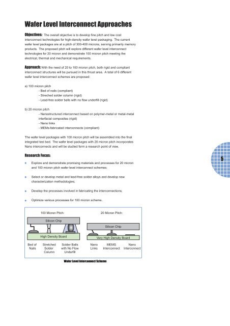
<strong>Wafer</strong> <strong>Level</strong> Interconnect ApproachesObjectives: The overall objective is to develop fine pitch and low costinterconnect technologies for high-density wafer level packaging. The currentwafer level packages are at a pitch <strong>of</strong> 300-400 microns, serving primarily memoryproducts. The proposed pitch will explore different wafer level interconnecttechnologies for 20 micron and demonstrate 100 micron pitch meeting theelectrical, thermal and mechanical requirements.Approach: With the need <strong>of</strong> 20 to 100 micron pitch, both rigid and compliantinterconnect structures will be pursued in this thrust area. A total <strong>of</strong> 6 differentwafer level interconnect schemes are proposed:a) 100 micron pitch- Bed <strong>of</strong> nails (compliant)- Streched solder column (rigid)- Lead-free solder balls with no flow underfill (rigid)b) 20 micron pitch- <strong>Nano</strong>structured interconnect based on polymer-metal or metal-metalinterfacial composites (rigid)- <strong>Nano</strong> links- MEMs-fabricated interconnects (compliant)The wafer level packages with 100 micron pitch will be assembled into the finalintegrated test bed. The wafer level packages with 20 micron pitch incorporates<strong>Nano</strong> interconnects and will be studied form a research point <strong>of</strong> view.Research Focus:Explore and demonstrate promising materials and processes for 20 micronand 100 micron pitch wafer level interconnect schemes;5Select or develop metal and lead-free solder alloys and develop newcharacterization methodologies;Develop the processes involved in fabricating the interconnections;Optimize various processes for 100 micron scheme.100 Micron Pitch: 20 Micron Pitch:Silicon ChipSilicon ChipHigh Density BoardVery High Density BoardBed <strong>of</strong>NailsStretchedSolderColumnSolder Ballswith No FlowUnderfill<strong>Nano</strong>LinksMEMSInterconnect<strong>Nano</strong>Interconnect<strong>Wafer</strong> <strong>Level</strong> Interconnect Scheme