Packaging Nano Wafer Level - National University of Singapore
Packaging Nano Wafer Level - National University of Singapore
Packaging Nano Wafer Level - National University of Singapore

Create successful ePaper yourself
Turn your PDF publications into a flip-book with our unique Google optimized e-Paper software.
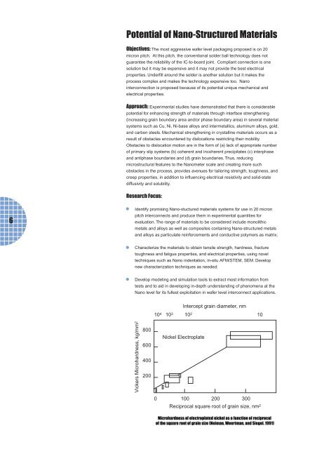
Potential <strong>of</strong> <strong>Nano</strong>-Structured MaterialsObjectives: The most aggressive wafer level packaging proposed is on 20micron pitch. At this pitch, the conventional solder ball technology does notguarantee the reliability <strong>of</strong> the IC-to-board joint. Compliant connection is onesolution but it may be expensive and it may not provide the best electricalproperties. Underfill around the solder is another solution but it makes theprocess complex and makes the technology expensive too. <strong>Nano</strong>interconnection is proposed because <strong>of</strong> its potential unique mechanical andelectrical properties.Approach: Experimental studies have demonstrated that there is considerablepotential for enhancing strength <strong>of</strong> materials through interface strengthening(increasing grain boundary area and/or phase boundary area) in several materialsystems such as Cu, Ni, Ni-base alloys and intermetallics, aluminum alloys, gold,and carbon steels. Mechanical strengthening in crystalline materials occurs as aresult <strong>of</strong> obstacles encountered by dislocations restricting their mobility.Obstacles to dislocation motion are in the form <strong>of</strong> (a) lack <strong>of</strong> appropriate number<strong>of</strong> primary slip systems (b) coherent and incoherent precipitates (c) interphaseand antiphase boundaries and (d) grain boundaries. Thus, reducingmicrostructural features to the <strong>Nano</strong>meter scale and creating more suchobstacles in the process, provides avenues for tailoring strength, toughness, andcreep properties, in addition to influencing electrical resistivity and solid-statediffusivity and solubility.Research Focus:6Identify promising <strong>Nano</strong>-stuctured materials systems for use in 20 micronpitch interconnects and produce them in experimental quantities forevaluation. The range <strong>of</strong> materials to be considered include monolithicmetals and alloys as well as composites containing <strong>Nano</strong>-structured metalsand alloys as particulate reinforcements and conductive polymers as matrix;Characterize the materials to obtain tensile strength, hardness, fracturetoughness and fatigue properties, and electrical properties, using noveltechniques such as <strong>Nano</strong> indentation, in-situ AFM/STEM, SEM. Developnew characterization techniques as needed;Develop modeling and simulation tools to extract most information fromtests and to aid in developing in-depth understanding <strong>of</strong> phenomena at the<strong>Nano</strong> level for its fullest exploitation in wafer level interconnect applications.Intercept grain diameter, nm10 4 10 3 10 2 10Vickers Microhardness, kg/mm 2800600400200Nickel Electroplate0 100 200 300Reciprocal square root <strong>of</strong> grain size, nm 2Microhardness <strong>of</strong> electroplated nickel as a function <strong>of</strong> reciprocal<strong>of</strong> the square root <strong>of</strong> grain size (Neiman, Weertman, and Siegel, 1991)