Packaging Nano Wafer Level - National University of Singapore
Packaging Nano Wafer Level - National University of Singapore
Packaging Nano Wafer Level - National University of Singapore

You also want an ePaper? Increase the reach of your titles
YUMPU automatically turns print PDFs into web optimized ePapers that Google loves.
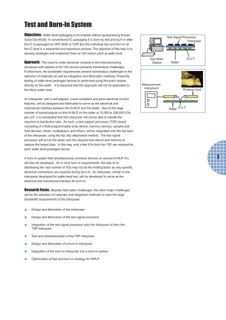
Test and Burn-In SystemObjectives: <strong>Wafer</strong> level packaging is incomplete without guaranteeing KnownGood Die (KGD). In conventional IC packaging it is done by test and burn in afterthe IC is packaged as QFP, BGA or CSP. But this individual test and burn-in atthe IC level is a sequential and expensive process. The objective <strong>of</strong> this task is todevelop strategies and implement them at 100 micron pitch at wafer level.Approach: The need to make electrical contacts to the interconnectingstructures with pitches <strong>of</strong> 20-100 microns presents tremendous challenges.Furthermore, the bandwidth requirements present tremendous challenges to theselection <strong>of</strong> materials as well as integration and fabrication methods. Presently,testing <strong>of</strong> wafer-level packaged devices is performed using fine-pitch probesdirectly on the wafer. It is expected that this approach will not be applicable tothe <strong>Nano</strong> wafer level.Test WorkStationMeasurementInstrumentTest Signal ProcessorInterposerD.U.T.<strong>Wafer</strong>Probing CardAn interposer, with a self-aligned, z-axis compliant and good electrical contactfeatures, will be designed and fabricated to serve as the electrical andmechanical interface between the N-WLP and the tester. Due to the largenumber <strong>of</strong> inputs/outputs on this N-WLP (in the order <strong>of</strong> 10,000 to 200,000 I/Osper cm 2 , it is anticipated that this interposer will not be able to handle therequired re-distribution task. As such, a test support processor (TSP) boardconsisting <strong>of</strong> a field-programmable array device, memory devices, sample-andholddevices, clocks, multiplexers, and others, will be integrated onto the top layer<strong>of</strong> the interposer, using the flip chip attachment method. The test signalprocessor will act as the tester with the required test stimuli and memory tocapture the tested data. In this way, only a few I/Os from the TSP are required foreach wafer level-packaged device.A burn-in system that simultaneously connects devices on several N-WLP ICswill also be developed. As in most burn-in requirements, the task <strong>of</strong> redistributingthe vast number <strong>of</strong> I/Os may not be the limiting factor as only specificelectrical connections are required during burn-in. An interposer, similar to theinterposer developed for wafer-level test, will be developed to serve as theelectrical and mechanical interface for burn-in.<strong>Wafer</strong> D.U.T.7Research Focus: Besides fabrication challenges, the other major challengeswill be the selection <strong>of</strong> materials and integration methods to meet the largebandwidth requirements <strong>of</strong> the interposer.Design and fabrication <strong>of</strong> the interposerDesign and fabrication <strong>of</strong> the test signal processorIntegration <strong>of</strong> the test signal processor onto the interposer to form theTSP interposerTest and characterization <strong>of</strong> the TSP interposerDesign and fabrication <strong>of</strong> a burn-in interposerIntegration <strong>of</strong> the burn-in interposer into a burn-in systemOptimization <strong>of</strong> test and burn-in strategy for NWLP