MEMC Glossary - MEMC Electronic Materials, Inc.
MEMC Glossary - MEMC Electronic Materials, Inc.
MEMC Glossary - MEMC Electronic Materials, Inc.
Create successful ePaper yourself
Turn your PDF publications into a flip-book with our unique Google optimized e-Paper software.
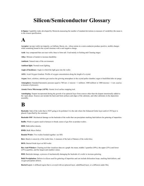
Silicon/Semiconductor <strong>Glossary</strong>6-Sigma: Capability index developed by Motorola measuring the number of standard deviations (a measure of variability) the mean isto the closest specification.AAcceptor: (p-type wafer) an impurity, as Gallium, Boron, etc., whose atoms in a semi-conductor produce positive, mobile chargeswhile remaining bound in the crystal structure with a unit negative charge.Acid: Any compound that can react with a base to form salt. Used mainly in Etching and Cleaning stages.Alloy: Mixture of metals to increase durability.Ambient: Natural state of the environment.Ambient light: Normal room lighting.Angle of <strong>Inc</strong>idence: Angle in which the light goes into the wafer.AOG: Axial Oxygen Gradient. Profile of oxygen concentration along the length of a crystal.Argon: Inert, colorless, odorless gas used as the growing atmosphere in the crystal puller chamber; argon is backfilled after air purge.Atmosphere: Standard barometric pressure equal to 760 torr. (1 micron = 1 millitorr, 1000 millitorr or 1000 microns = 1 torr, used asa measure of pressure).Atomic Force Microscope (AFM): Atomic level surface mapping tool.Autodoping: Dopant incorporated during the growth of an epitaxial layer from sources other than the dopant intentionally added tothe vapor phase. Sources can include the back and front surfaces and edges of the substrate, and other substrates in the depositionassembly.BBackside: Side of the wafer that is NOT going to be polished. It is the side where the Enhanced Getter layer and/or LTO layer isplaced if specified by the customer.Backside OSF: Mechanical damage on the backside of the wafer that can precipitate stacking fault defects for gettering of impurities.Baffle: Wafer or quartz used in furnaces to break course of gas flow at product wafers.BDD: Bulk defect density.BMD: Bulk Micro Defect.Bonded Wafer: Two wafers bonded together: see SOI.Bow: Bend or concavity of the wafer/slice. A measure of the lack of flatness of the wafer/slice.BOX: Buried Oxide layer on SOI wafer.Box-And-Whisker: Charting tool that visualizes data on a graph: the mean, middle 2 quartiles (50%), the upper (25%) and lower(25%) quartiles, and the largest and smallest values.BSD: Backside damage, a process of mechanically damaging the backside of a wafer to increase gettering.Bulk Precipitation: Defects in silicon used for gettering of impurities and can include dislocation loops, stacking fault defects, andoxygen precipitate defects.Buried Layer: A diffused region that is covered with an epitaxial layer, subdiffused layer, or a diffusion under film.
Bvox: Breakdown voltage test of oxide layer grown on wafers, sister test to GOI.CCantilever: Ceramic or silicon carbide rod or silicon carbide paddle that holds the quartz boats. This device is supported at one end.In this case, it is the door end and has the same function as a sled.Capability Index: Value to measure how capable a product or process is at meeting a specification.Carbon Beam: Length of carbon approximately 2" wide attached to the bottom of an ingot. In the slicing process the carbon allowsthe saw to cut completely through the silicon. The beam remains intact to hold the wafers until the preset number of wafers have beencut.Carriers: Stainless steel apparatus used to contain wafers during the lapping process.Cassette: Compact case designed to segregate slices for process handling and shipping.Chamfer: Beveled edge.Charge: Specified quantity of poly to be loaded into the crystal puller.Cleanroom: Controlled areas with a low particle size/count where the latter part of wafer production takes place. The below tableshows how classes are defined, with class 1 being the cleanest environment.Class: # of particles allowed in a cubic foot of room air.Particle Size1 (means it can have no more than 1 particle) 0.5 micron or greater10 0.5 micron or greater100 (means it can have no more than 100 particles) 0.5 micron or greater1000 0.5 micron or greater10,000 0.5 micron or greater(One eyelash is about 100 microns in diameter)Cleavage Plane: A break along crystal planes determined by crystal structure and always parallel to such a plane.CMP: (Chemical-Mechical Polish) A process of removing surface material using chemical and mechanical means to achieve a mirrorlikesurface in preparation for subsequent processing.Collimated Light: Light source in which the rays are parallel. Used for surface inspection of wafers.Conductivity: A measure of the ease with which electrical carriers flow in a material: the reciprocal of Resistivity.Conductivity Type: Defines the nature of the majority of carriers in the material: either N-type or P-type.Contamination: Foreign matter in the silicon, other than polysilicon and dopant, that can cause loss of structure (atom alignment)during the growing process.COP: Crystal Originated Pits.Cp: Capability potential index which measures the width of two specifications in respect to six standard deviations.Cpk: Statistical parameter used to compare product distribution to spec limits. A capability potential index measuring the distancefrom the mean to the nearest specification in respect to three standard deviations.Crucible: Container made of quartz for holding the poly charge inside the crystal puller.Crystal: A natural or synthetic semiconductor material whose atoms are arranged with some degree of geometric regularity. A solidcomposed of atoms, ions, or molecules arranged in a pattern that is periodic in three dimensions.Crystal Puller: Machine designed to pull/grow electronic grade silicon under controlled parameters and within set specifications.Crystallographic Orientation: There are three orientation planes in the silicon crystal: , , and . The orientation ofthe wafer is classified by which orientation plane the surface of the wafer is parallel to. The surface might not be exactly parallel, butslightly different, and the difference is called the displacement angle or off angle orientation. The relationship between the crystal'sorientation and the radius is marked by either a notch or a flat cut into the wafer.
Cubic Feet per Minute (CFM): Volumetric flow rate used to meter gases.CVD (Chemical Vapor Deposition): Formation of a solid film on a substrate through the reaction of gas-phase reactants (precursors)that contain the required constituents.Czochralski (CZ): Crystal growing process that was named after the inventor.DDefect Free Region: The linear distance from the frontside wafer surface to the depth of the first bulk defect.Degree: Unit of measuring angles when orienting an ingot.Design of Experiments (DOE): Method to design, run and analyze an experiment to maximize information and minimize testing.Diameter: Straight-line measurement drawn through the center of a circle or sphere from one side to the other.Diffusion: A method of doping or modifying the characteristics of semiconductor material by "baking" wafers of the basesemiconductor material in furnaces with controlled atmospheres of impurity materials.Diffusion Length: The distance a front side free-electron or hole can travel through a crystal. This is proportional to the Lifetime ofthe crystal.Dislocation: A class of one-dimensional, or line defects in silicon crystals.DNZ (Denuded Zone Depth): The linear distance from the frontside wafer surface to the depth where the defect density appearsnearly uniform.Donor: Atom, usually an impurity in silicon, that acts as an electron source. It contributes an extra electron to the crystal structure.Most common is phosphorus.Dopant: Element added to silicon decreasing its resistivity. Silicon, by itself does not conduct electricity. Boron is usually used for p-type and phosphorus is usually used for n-type.Doping or Dopant: Chemical impurities added to polysilicon which will yield either n- or p-type silicon, depending on the specificdopant used.EEdge Crown: The difference between the surface elevation 1/8" (3.2mm) from the edge of the slice and the elevation of the sliceedges exposed in microns (associated with epi layer deposition).Edge Exclusion: Narrow band on the outside edge of the wafer that does not have an oxide coating.Edge Grinding: Process that bevels the edges of the slices to strengthen them.Ellipsometer: Optical measuring device used to measure oxide and nitride thickness, as well as, the index of refraction.Epi: (epitaxial or epitaxy process) Depositing a thin layer of silicon atoms onto a wafer by condensing a controlled amount of silicongas (silane) onto the polished surface of the wafer in a temperature-controlled environment.Epitaxial Layer: The layer or layers of semiconductor material having the same crystalline orientation as the host substrate on whichit is grown.Endcone or Bottom: Gradual decreases in diameter until the silicon forms a point at the end of the growing/pulling process. As a ruleof thumb, the bottom/endcone should be grown the length of the rod’s diameter to allow for shock back or undesirable structure.Etch: To remove or dissolve surface contamination, work-damaged material (polishing), and to control thickness by chemical actionwith strong acid and alkaline compounds.Etch – Mirror: Used to create a clean, shiny finish for visual inspection and resistivity measurements.Etch – Preferential: An etch that exhibits an accelerated etch rate along specific crystallographic planes.Etch Rate: Rate of silicon removal in microns per minute.
FFace: Parallel lines along the surface of the crystal, also known as growth lines or ZD, zero defect, lines.Flat: Straight edge on the wafer’s outer perimeter. It is used to identify certain characteristics. (AKA the JLS).Flat (major): May be the only flat (straight edge) on the wafer. If there is more than one flat then it is the longest flat on the perimeterof the wafer.Flat (minor): Shortest flat (straight edge) on the wafer.Flatness: The maximum deviation of the wafer surface from a flat plane. Flatness measurement is usually done with the backside heldto a flat surface (a vacuum chuck) and excludes linear thickness variations.Focal Plane: That plane whose normal provides the shortest distance between the absolute maximum and absolute minimum on thewafer surface.Focal Plane Deviation (FPD): Maximum deviation of the wafer surface above and below the focal plane.FTIR: Fourier Transform Infrared, a means of measuring oxygen or carbon levels in the crystal.GGettering: Gettering is a process that attracts contaminents and traps defects when the wafers are heated. Can be initiated throughmechanical damage or interstial oxygen. Extrinsic gettering is caused by BSD. Intrinsic gettering is caused by interstial oxygen.Global Flatness: Overall flatness of the wafer.Grind: Abrade/remove material by grinding; rod diameter reduction method to specifications and for flattening.GFA: Gas Fusion Analysis, a means of testing oxygen or carbon levels in the crystal.GOI: Gate Oxide IntegrityHHaze: Light scattering caused by microscopic surface irregularities (such as a high concentration of pits, mounds, small ridges,particles, etc.) on epitaxial wafers or polished slices.Hillocks: Defect in the surface of the wafer resembling a hill; cannot be seen with the naked eye.IIngot: A semiconductor grown cylinder, polycrystalline or single crystal, generally of irregular diameter or in the as-grown state.Integrated circuits: Tiny complex electronic components and their connections produced on a silicon slice.Interstitial: Relating to crystalline compound in which small atoms or ions of a nonmetal occupy holes between the larger metalatoms and ions in the crystal lattice.JJLS (Joseph Larry Schaefer): Method of physically identifying a wafer. Major flats, minor flats and notches are ground on thesilicon rod before it is cut. These markings identify the molecular orientation.
KKerf: The notch left by a saw cut; the width of a saw cut.Kerf Loss: The amount of material lost while slicing wafers. The kerf is the cut and swarf is the chips and fillings from the kerf.LLapping: Process to remove controlled amounts of silicon from the slice using a lapping compound. This process removes sawdamage and positively impacts the slice’s flatness.Laser mark: Method of identification required by some customers. Series of letters and numbers inscribed onto the wafer by laser.Lifetime: The average time a free-electron or hole can exist in a crystal, measured in seconds. Lifetime may vary within a crystal:bulk lifetime within the crystal and surface lifetime at, of course, the surface.Linear Thickness Variation: Thickness variation within a slice whose front and back surfaces can be represented by two, nonparallelplanes.Local or Site Flatness: Flatness of specifically defined areas on the slice.Lot: Group of wafers going to the same area with the same identities and are to be processed together.Low Temperature Oxide (LTO): Sealant to keep the dopant in the wafer when it goes through the Epi process. It is applied inFurnace/Enhanced Gettering Area.LPCVD: Low Pressure CVD, deposits a layer of polysilicon to the wafer, later removed by polishing. A backside layer can act as agettering agent.LPD: Light Particle Defect, sometimes known as particles.MMelt: The pure, molten silicon from which single crystal silicon is grown in a crystal pulling furnace during the Czochralski process.Meltdown: Changing a polysilicon charge from a solid to a liquid state by heating it in the crystal puller.Micron: A unit of length, 1/1,000,000 (one millionth) of a meter.MOScap: Test structure used for Bvox, GOI, VTW, and Zerbst tests. Capacitor structure: silicon wafer/gate oxide/polysilicon gate.NNanotopology: Surface variations over a small areaN-Type: Property of the silicon semiconductor material. Doping with donor atoms increases the density of negative charge carriers(electrons) in the conduction band and produces an N-type semiconductor.Neck: Portion of the crystal below the seed and above the taper. The first growth step in a crystal.OOhm: Unit of electrical resistance.Oi: Interstitial Oxygen.Opposite End (OE): End of the grown crystal rod. Known more formally as the ‘tang’ portion of the rod.Optical Comparator: Instrument held close to the wafer’s edge for evaluation of the edge grinding process.Optical Precipitation Profiler (OPP): Non-destructive measurement of bulk defects.
SEMI: Semiconductor Equipment and <strong>Materials</strong> Institute. Sets specifications for the semiconductor industry.Silicon: Tetravalent nonmetallic element that occurs combined as the most abundant element next to oxygen in the earth’s crust andis used in alloys and electronic devices.Single Crystal: When the atoms in the crystal are all aligned in the same way.Slip: A process of plastic deformation in which one part of the crystal undergoes a shear displacement relative to another in a fashionthat preserves the crystallinity of the material. The direction is on a specific crystallographic plane.Slug: Thick piece of silicon, usually a wedge cut, used to test the material characteristics for customer specs.Slurry: Solid suspension in liquid used for slicing, lapping, and polishing.SOI: Silicon on Insulator, usually achieved by bonding two wafers, one of which has oxide on top.SRP - Spreading Resistance Profiling: The resistance measured between the conductive metal of a point probe and a large area,relatively low-resistance semiconductor contact, dominated by the resistivity of the semiconductor volume close to the problem.Stacking Faults: Pyramid shaped imperfections in the silicon wafer.Substrate: Basic surface on which a material adheres. A single-crystal slice that is the basis for subsequent processing operations,such as epi layer deposition, diffusion, ion implants, etc.Surface Photovoltage (SPV): test for recombination minority carrier lifetime.Swirl: Shallow pits looked for during visual inspection. Helical or concentric features that are visible to the unaided eye afterpreferential etch, and appear to be discontinuous under 150x magnification.TTaper: A measure of the flatness of a wafer, taper being thicker at the edges than at the center.Thickness: Cross sectional depth of a silicon slice measured in mils (1 mil = 0.001 inch).TIR: Total Indicator Reading, the distance between the highest and lowest point on the wafer surface measured normal to the focalplane.Total Thickness Variation (TTV): variation of thickness from the center and both sides of the wafer.UVWWarp: Maximum distance from the lowest point to the highest point on the wafer’s surface.X
RFC 3875 CGI Version 1.1 October 2004or transport level authentication and security. The server MAY also function in a ‘non-transparent’ manner,modifying the request or response in order to provide some additional service, such as media type transformationor protocol reduction.The server MUST perform translations and protocol conversions on the client request data required by this specification.Furthermore, the server retains its responsibility to the client to conform to the relevant network protocoleven if the CGI script fails to conform to this specification.If the server is applying authentication to the request, then it MUST NOT execute the script unless the requestpasses all defined access controls.3.2 Script SelectionThe server determines which CGI is script to be executed based on a generic-form URI supplied by the client.This URI includes a hierarchical path with components separated by “/”. For any particular request, the serverwill identify all or a leading part of this path with an individual script, thus placing the script at a particular pointin the path hierarchy. The remainder of the path, if any, is a resource or sub-resource identifier to be interpretedby the script.Information about this split of the path is available to the script in the meta-variables, described below. Supportfor non-hierarchical URI schemes is outside the scope of this specification.3.3 The Script-URIThe mapping from client request URI to choice of script is defined by the particular server implementation and itsconfiguration. The server may allow the script to be identified with a set of several different URI path hierarchies,and therefore is permitted to replace the URI by other members of this set during processing and generation of themeta-variables. The server1. MAY preserve the URI in the particular client request; or2. it MAY select a canonical URI from the set of possible values for each script; or3. it can implement any other selection of URI from the set.From the meta-variables thus generated, a URI, the ‘Script-URI’, can be constructed. This MUST have theproperty that if the client had accessed this URI instead, then the script would have been executed with the samevalues for the SCRIPT_NAME, PATH_INFO and QUERY_STRING meta-variables. The Script-URI has thestructure of a generic URI as defined in section 3 of RFC 2396 [2], with the exception that object parametersand fragment identifiers are not permitted. The various components of the Script-URI are defined by some of themeta-variables (see below);script-URI = "://" ":" "?" Robinson & Coar Informational [Page 8]


