L296 L296P - Soemtron.org
L296 L296P - Soemtron.org
L296 L296P - Soemtron.org
- No tags were found...

Create successful ePaper yourself
Turn your PDF publications into a flip-book with our unique Google optimized e-Paper software.
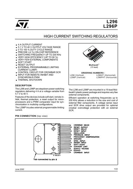
®<strong>L296</strong><strong>L296</strong>PHIGH CURRENT SWITCHING REGULATORS4 A OUTPUT CURRENT5.1 V TO 40 V OUTPUT VOLTAGE RANGE0 TO 100 % DUTY CYCLE RANGEPRECISE (±2 %) ON-CHIP REFERENCESWITCHING FREQUENCY UP TO 200 KHzVERY HIGH EFFICIENCY (UP TO 90 %)VERY FEW EXTERNAL COMPONENTSSOFT STARTRESET OUTPUTEXTERNAL PROGRAMMABLE LIMITINGCURRENT (<strong>L296</strong>P)CONTROL CIRCUIT FOR CROWBAR SCR.INPUT FOR REMOTE INHIBIT ANDSYNCHRONUS PWMTHERMAL SHUTDOWNDESCRIPTIONThe <strong>L296</strong> and <strong>L296</strong>P are stepdown power switchingregulators delivering 4 A at a voltage variable from5.1 V to 40 V.Features of the devices include soft start, remote inhibit,thermal protection, a reset output for microprocessorsand a PWM comparator input for synchronizationin multichip configurations.The <strong>L296</strong>P incudes external programmable limitingcurrent.Multiwatt ®(15 lead)ORDERING NUMBERS :<strong>L296</strong> (Vertical)<strong>L296</strong>HT (Horizontal)<strong>L296</strong>P (Vertical)<strong>L296</strong>PHT (Horizontal)The <strong>L296</strong> and <strong>L296</strong>P are mounted in a 15-lead Multiwatt®plastic power package and requires very fewexternal components.Efficient operation at switching frequencies up to200 KHz allows a reduction in the size and cost ofexternal filter components. A voltage sense inputand SCR drive output are provided for optionalcrowbar overvoltage protection with an externalSCR.PIN CONNECTION (top view)June 20001/22
<strong>L296</strong> - <strong>L296</strong>PPIN FUNCTIONSN° Name Function1 CROWBAR INPUT Voltage Sense Input for Crowbar Overvoltage Protection. Normally connected to thefeedback input thus triggering the SCR when V out exceeds nominal by 20 %. Mayalso monitor the input and a voltage divider can be added to increase the threshold.Connected to ground when SCR not used.2 OUTPUT Regulator Output3 SUPPLY VOLTAGE Unrergulated Voltage Input. An internal Regulator Powers the <strong>L296</strong>s Internal Logic.4 CURRENT LIMIT A resistor connected between this terminal and ground sets the current limiterthreshold. If this terminal is left unconnected the threshold is internally set (seeelectrical characteristics).5 SOFT START Soft Start Time Constant. A capacitor is connected between this terminal and groundto define the soft start time constant. This capacitor also determines the averageshort circuit output current.6 INHIBIT INPUT TTL – Level Remote Inhibit. A logic high level on this input disables the device.7 SYNC INPUT Multiple <strong>L296</strong>s are synchronized by connecting the pin 7 inputs together and omittingthe oscillator RC network on all but one device.8 GROUND Common Ground Terminal9 FREQUENCYCOMPENSATIONA series RC network connected between this terminal and ground determines theregulation loop gain characteristics.10 FEEDBACK INPUT The Feedback Terminal on the Regulation Loop. The output is connected directly tothis terminal for 5.1V operation ; it is connected via a divider for higher voltages.11 OSCILLATOR A parallel RC networki connected to this terminal determines the switching frequency.This pin must be connected to pin 7 input when the internal oscillator is used.12 RESET INPUT Input of the Reset Circuit. The threshold is roughly 5 V. It may be connected to thefeedback point or via a divider to the input.13 RESET DELAY A capacitor connected between this terminal and ground determines the reset signaldelay time.14 RESET OUTPUT Open collector reset signal output. This output is high when the supply is safe.15 CROWBAR OUTPUT SCR gate drive output of the crowbar circuit.BLOCK DIAGRAM2/22
<strong>L296</strong> - <strong>L296</strong>PCIRCUIT OPERATION(refer to the block diagram)The <strong>L296</strong> and <strong>L296</strong>P are monolithic stepdownswitching regulators providing output voltages from5.1V to 40V and delivering 4A.The regulation loop consists of a sawtooth oscillator,error amplifier, comparator and the output stage. Anerror signal is produced by comparing the outputvoltage with a precise 5.1V on-chip reference (zenerzap trimmed to ± 2 %). This error signal is then comparedwith the sawtooth signal to generate the fixedfrequency pulse width modulated pulses which drivethe output stage. The gain and frequency stability ofthe loop can be adjusted by an external RC networkconnected to pin 9. Closing the loop directly gives anoutput voltage of 5.1V. Higher voltages are obtainedby inserting a voltage divider.Output overcurrents at switch on are prevented bythe soft start function. The error amplifier output isinitially clamped by the external capacitor Css andallowed to rise, linearly, as this capacitor is chargedby a constant current source.Output overload protection is provided in the form ofa current limiter. The load current is sensed by aninternal metal resistor connected to a comparator.When the load current exceeds a preset thresholdthis comparator sets a flip flop which disables theoutput stage and discharges the soft start capacitor.A second comparator resets the flip flop when thevoltage across the soft start capacitor has fallen toFigure 1 : Reset Output Waveforms0.4V. The output stage is thus re-enabled and theoutput voltage rises under control of the soft startnetwork. If the overload condition is still present thelimiter will trigger again when the threshold currentis reached. The average short circuit current is limitedto a safe value by the dead time introduced bythe soft start network.The reset circuit generates an output signal whenthe supply voltage exceeds a threshold programmedby an external divider. The reset signal isgenerated with a delay time programmed by an externalcapacitor. When the supply falls below thethreshold the reset output goes low immediately.The reset output is an open collector.The scrowbar circuit senses the output voltage andthe crowbar output can provide a current of 100mAto switch on an external SCR. This SCR is triggeredwhen the output voltage exceeds the nominal by20%. There is no internal connection between theoutput and crowbar sense input therefore the crowbarcan monitor either the input or the output.A TTL - level inhibit input is provided for applicationssuch as remote on/off control. This input is activatedby high logic level and disables circuit operation. Afteran inhibit the <strong>L296</strong> restarts under control of thesoft start network.The thermal overload circuit disables circuit operationwhen the junction temperature reaches about150 °C and has hysteresis to prevent unstable conditions.3/22
<strong>L296</strong> - <strong>L296</strong>PFigure 2 : Soft Start WaveformsFigure 3 : Current Limiter WaveformsABSOLUTE MAXIMUM RATINGSSymbol Parameter Value UnitV i Input Voltage (pin 3) 50 VV i – V 2 Input to Output Voltage Difference 50 VV 2Output DC VoltageOutput Peak Voltage at t = 0.1 µsec f = 200KHzV 1, V 12 Voltage at Pins 1, 12 10 VV 15 Voltage at Pin 15 15 VV 4, V 5, V 7, V 9, V 13 Voltage at Pins 4, 5, 7, 9 and 13 5.5 VV 10 , V 6 Voltage at Pins 10 and 6 7 VV 14 Voltage at Pin 14 (I 14 ≤ 1 mA) V iI 9 Pin 9 Sink Current 1 mAI 11 Pin 11 Source Current 20 mAI 14 Pin 14 Sink Current (V 14 < 5 V) 50 mAP tot Power Dissipation at T case ≤ 90 °C 20 WT j, T stg Junction and Storage Temperature – 40 to 150 °C– 1– 7VV4/22
<strong>L296</strong> - <strong>L296</strong>PTHERMAL DATASymbol Parameter Value UnitR th j-case Thermal Resistance Junction-case Max. 3 °C/WR th j-amb Thermal Resistance Junction-ambient Max. 35 °C/WELECTRICAL CHARACTERISTICS(refer to the test circuits Tj = 25 o C, Vi = 35V, unless otherwise specified)Symbol Parameter Test Conditions Min. Typ. Max. Unit Fig.DYNAMIC CHARACTERISTICS (pin 6 to GND unless otherwise specified)V o Output Voltage Range V i = 46V, I o = 1A V ref 40 V 4V i Input Voltage Range V o = V ref to 36V, I o ≤ 3A 9 46 V 4V i Input Voltage Range Note (1), V o = V REF to 36V I o = 4A 46 V 4∆V o Line Regulation V i =10V to 40V, V o = V ref, I o = 2A 15 50 mV 4∆V o Load Regulation V o = V refI o = 2A to 4AI o = 0.5A to 4A10153045mV 4V ref Internal Reference Voltage (pin 10) V i = 9V to 46V, I o = 2A 5 5.1 5.2 V 4∆ V ref Average Temperature Coefficient T j = 0°C to 125°C, I o = 2A 0.4 mV/°C∆ T of Reference VoltageV d Dropout Voltage Between Pin 2and Pin 3I o = 4AI o = 2AI 2L Current Limiting Threshold (pin 2) <strong>L296</strong> - Pin 4 Open,V i = 9V to 40V, V o = V ref to 36V<strong>L296</strong>P - V i = 9V to 40V, V o = V refPin 4 OpenR Iim = 22kΩ21.33.22.1VV444.5 7.5 A 452.574.5A 4I SH Input Average Current V i = 46V, Output Short-circuited 60 100 mA 4η Efficiency I o = 3 AV o = V refV o = 12V7585% 4SVR Supply Voltage Ripple Rejection ∆V i = 2 V rms , f ripple = 100Hz 50 56 dB 4V o = V ref, I o = 2Af Switching Frequency 85 100 115 kHz 4∆ f∆ V i∆ f∆ T jf maxT sdVoltage Stability of SwitchingFrequencyTemperature Stability of SwitchingFrequencyMaximum Operating SwitchingFrequencyThermal Shutdown JunctionTemperatureDC CHARACTERISTICSI 3Q Quiescent Drain Current V i = 46V, V 7 = 0V, S1 : B, S2 : BV 6 = 0VV 6 = 3V– I 2L Output Leakage Current V i = 46V, V 6 = 3V, S1 : B, S2 : A,V 7 = 0VV i = 9V to 46V 0.5 % 4T j = 0°C to 125°C 1 % 4V o = V ref , I o = 1A 200 kHz –Note (2) 135 145 °C –66308540mA2 mANote(1) : Using min. 7 A schottky diode.(2) : Guaranteed by design, not 100 % tested in production.5/22
<strong>L296</strong> - <strong>L296</strong>PELECTRICAL CHARACTERISTICS (continued)Symbol Parameter Test Conditions Min. Typ. Max. Unit Fig.SOFT STARTI 5 so Source Current V 6 = 0V, V 5 = 3V 80 130 150 µA 6bI 5 si Sink Current V 6 = 3V, V 5 = 3V 50 70 120 µA 6bINHIBITV 6LV 6HInput VoltageLow LevelHigh LevelInput Currentwith Input Voltage– I 6L Low Level– I 6H High LevelV i = 9V to 46V, V 7 = 0V,S1 : B, S2 : B – 0.32V i = 9V to 46V, V 7 = 0V,S1 : B, S2 : BV 6 = 0.8VV 6 = 2V0.85.5V6a103µA 6aERROR AMPLIFIERV 9H High Level Output Voltage V 10 = 4.7V, I 9 = 100µA,3.5 V 6cS1 : A, S2 : AV 9L Low Level Output Voltage V 10 = 5.3V, I 9 = 100µA,0.5 V 6cS1 : A, S2 : EI 9 si Sink Output Current V 10 = 5.3V, S1 : A, S2 : B 100 150 µA 6c– I 9 so Source Output Current V 10 = 4.7V, S1 : A, S2 : D 100 150 µA 6cI 10 Input Bias Current V 10 = 5.2V, S1 : BV 10 = 6.4V, S1 : B, <strong>L296</strong>PG v DC Open Loop Gain V 9 = 1V to 3V, S1 : A, S2 : C 46 55 dB 6cOSCILLATOR AND PWM COMPARATOR– I 7 Input Bias Current of V 7 = 0.5V to 3.5V 5 µA 6aPWM Comparator– I 11 Oscillator Source Current V 11 = 2V, S1 : A, S2 : B 5 mARESETV 12 R Rising Threshold VoltageV ref V ref V ref V 6dV 12 F Falling Threshold VoltageV i = 9V to 46V,S1 : B, S2 : B-150mV4.75-100mVV ref-50mVV ref V 6d-150mV -100mVV 13 D Delay Thershold Voltage4.3 4.5 4.7 V 6dV 13 H Delay Threshold Voltage V 12 = 5.3V, S1 : A, S2 : B100 mV 6dHysteresisV 14 S Output Saturation Voltage I 14 = 16mA, V 12 = 4.7V, S1, S2 : B 0.4 V 6dI 12 Input Bias Current V 12 = 0V to V ref , S1 : B, S2 : B 1 3 µA 6d– I 13 soI 13 siDelay Source CurrentDelay Sink CurrentV 13 = 3V, S1 : A, S2 : BV 12 = 5.3VV 12 = 4.7V7010221010µAµA110 140 µAmAI 14 Output Leakage Current V i = 46V, V 12 = 5.3V, S1 : B, S2 : A 100 µA 6dCROWBARV 1 Input Threshold Voltage S1 : B 5.5 6 6.4 V 6bV 15 Output Saturation Voltage V i = 9V to 46V, V i = 5.4V,0.2 0.4 V 6bI 15 = 5mA, S1 : AI 1 Input Bias Current V 1 = 6V, S1 : B 10 µA 6b– I 15 Output Source Current V i = 9V to 46V, V 1 = 6.5V,V 15 = 2V, S1 : B70 100 mA 6b6c6c6d6/22
<strong>L296</strong> - <strong>L296</strong>PFigure 4 : Dynamic Test CircuitC7, C8 : EKR (ROE)L1 : L = 300 µH at 8 A Core type : MAGNETICS 58930 - A2 MPPN° turns : 43 Wire Gauge : 1 mm (18 AWG) COGEMA 946044(*) Minimum suggested value (10 µF) to avoid oscillations. Ripple consideration leads to typical value of 1000 µF or higher.Figure 5 : PC. Board and Component Layout of the Circuit of Figure 4 (1:1 scale)7/22
<strong>L296</strong> - <strong>L296</strong>PFigure 6 : DC Test Circuits.Figure 6a. Figure 6b.Figure 6c.1 - Set V 10 FOR V 9 = 1 V2 - Change V10 to obtain V9 = 3 V3 - G V =DV9=2V∆V 10 ∆V 10Figure 6d.8/22
<strong>L296</strong> - <strong>L296</strong>PFigure 31 : Current Limiting Threshold vs. Rpin 4(<strong>L296</strong>P only).Figure 32 : Current Limiting Threshold vs. JunctionTemperature.Figure 33 : Current Limiting Threshold vs.Supply Voltage.13/22
<strong>L296</strong> - <strong>L296</strong>PAPPLICATION INFORMATIONFigure 34 : Typical Application Circuit.(*) Minimum value (10 µF) to avoid oscillations ; ripple consideration leads to typical value of 1000 µF or higher L1 : 58930 - MPP COGEMA946044 ; GUP 20 COGEMA 946045SUGGESTED INDUCTOR (L1)Core Type No Turns Wire Gauge Air GapMagnetics 58930 – A2MPP 43 1.0 mm –Thomson GUP 20 x 16 x 7 65 0.8 mm 1 mmSiemens EC 35/17/10 (B6633& – G0500 – X127) 40 2 x 0.8 mm –VOGT 250 µH Toroidal Coil, Part Number 5730501800Resistor Values for Standard Output VoltagesV 0 R8 R712 V15 V18 V24 V4.7 KΩ4.7 KΩ4.7 KΩ4.7 KΩ6.2 KΩ9.1 KΩ12 KΩ18 KΩ14/22
<strong>L296</strong> - <strong>L296</strong>PFigure 35 : P.C. Board and Component Layout of the Circuit of fig. 34 (1:1 scale)SELECTION OF COMPONENT VALUES (see fig. 34)ComponentR1R2RecommendedValue–100 kΩPurposeSet Input VoltageThreshold for Reset.Allowed RageMin. Max.–220kΩNotesR1/R2 V i min− 15If output voltage is sensed R1 andR2 may be limited and pin 12connected to pin 10.R3 4.3 kΩ Sets Switching Frequency 1 kΩ 100kΩR4 10 kΩ Pull-down Resistor 22kΩ May be omitted and pin 6 groundedif inhibit not used.R5 15 kΩ Frequency Compensation 10kΩR6Collector Load For ResetOutputV O0.05AOmitted if reset function not used.R7R8–4.7 kΩDivider to Set OutputVoltage–––1kΩR7/R8 = V O − V REFV REF-R iim – Sets Current Limit Level 7.5kΩ If R iim is omitted and pin 4 left openthe current limit is internally fixed.C1 10 µF Stability 2.2µFC2 2.2 µF Sets Reset Delay – – Omitted if reset function not used.C3 2.2 nF Sets Switching Frequency 1 nF 3.3nFC4 2.2 µF Soft Start 1 µF – Also determines average shortcircuit current.C5 33 nF Frequency CompensationC6 390 pF High FrequencyCompensation– – Not required for 5 V operation.C7, C8L1100 µF300 µHOutput Filter –100µHQ1 Crowbar Protection The SCR must be able to withstandthe peak discharge current of theoutput capacitor and the shortcircuit current of the device.D1 Recirculation Diode 7A Schottky or 35 ns t rr Diode.–15/22
<strong>L296</strong> - <strong>L296</strong>PFigure 36 : A Minimal 5.1 V Fixed Regulator. Very Few Components are Required.Figure 37 : 12 V/10 A Power Supply.16/22
<strong>L296</strong> - <strong>L296</strong>PFigure 38 : Programmable Power Supply.V o = 5.1 to 15 VI o = 4 A max. (min. load current = 100 mA)ripple ≤ 20 mVload regulation (1 A to 4 A) = 10 mV (V o = 5.1 V)line regulation (220 V ± 15 % and to I o = 3 A) = 15 mV (V o = 5.1 V)Figure 39 : Preregulator for Distributed Supplies.(*) L2 and C2 are necessary to reduce the switching frequency spikes.17/22
<strong>L296</strong> - <strong>L296</strong>PFigure 40 : In Multiple Supplies Several <strong>L296</strong>scan be Synchronized As Shown.Figure 41 : Voltage Sensing for Remote Load.Figure 42 : A 5.1 V/15 V/24 V Multiple Supply. Note the Synchronization of the Three <strong>L296</strong>s.18/22
<strong>L296</strong> - <strong>L296</strong>PFigure 43 : 5.1V/2A Power Supply using ExternalLimiting Current Resistor and CrowbarProtection on the Supply Voltage(<strong>L296</strong>P only)If these times are still too long, an external PNP transistormay be added, as shown in Figure 45 ; withthis circuit discharge times of a few microsecondsmay be obtained.Figure 45SOFT-START AND REPETITIVE POWER-ONWhen the device is repetitively powered-on, the softstartcapacitor, CSS, must be discharged rapidly toensure that each start is "soft". This can be achievedeconomically using the reset circuit, as shown in Figure44.In this circuit the divider R1, R2 connected to pin 12determines the minimum supply voltage, belowwhich the open collector transistor at the pin 14 outputdischarges CSS.Figure 44HOW TO OBTAIN BOTH RESET ANDPOWER FAILFigure 46 illustrates how it is possible to obtain at thesame time both the power fail and reset functionssimply by adding one diode (D) and one resistor (R).In this case the Reset delay time (pin 13) can onlystart when the output voltage is VO ≥ VREF - 100mVand the voltage accross R2 is higher than 4.5V.With the hysteresis resistor it is possible to fix the inputpin 12 hysteresis in order to increase immunityto the 100Hz ripple present on the supply voltage.Moreover, the power fail and reset delay time areautomatically locked to the soft-start. Soft-start anddelayed reset are thus two sequential functions.The hysteresis resistor should be In the range ofaboit 100kΩ and the pull-up resistor of 1 to 2.2kΩ.Figure 46The approximate discharge times obtained with thiscircuit are :CSS (µF)2.24.710tDIS (µs)20030060019/22
<strong>L296</strong> - <strong>L296</strong>PDIM.mminchMIN. TYP. MAX. MIN. TYP. MAX.A 5 0.197B 2.65 0.104C 1.6 0.063D 1 0.039E 0.49 0.55 0.019 0.022F 0.66 0.75 0.026 0.030G 1.02 1.27 1.52 0.040 0.050 0.060G1 17.53 17.78 18.03 0.690 0.700 0.710H1 19.6 0.772H2 20.2 0.795L 21.9 22.2 22.5 0.862 0.874 0.886L1 21.7 22.1 22.5 0.854 0.870 0.886L2 17.65 18.1 0.695 0.713L3 17.25 17.5 17.75 0.679 0.689 0.699L4 10.3 10.7 10.9 0.406 0.421 0.429L7 2.65 2.9 0.104 0.114M 4.25 4.55 4.85 0.167 0.179 0.191M1 4.63 5.08 5.53 0.182 0.200 0.218S 1.9 2.6 0.075 0.102S1 1.9 2.6 0.075 0.102Dia1 3.65 3.85 0.144 0.152OUTLINE ANDMECHANICAL DATAMultiwatt15 V20/22
<strong>L296</strong> - <strong>L296</strong>PDIM.mminchMIN. TYP. MAX. MIN. TYP. MAX.A 5 0.197B 2.65 0.104C 1.6 0.063E 0.49 0.55 0.019 0.022F 0.66 0.75 0.026 0.030G 1.14 1.27 1.4 0.045 0.050 0.055G1 17.57 17.78 17.91 0.692 0.700 0.705H1 19.6 0.772H2 20.2 0.795L 20.57 0.810L1 18.03 0.710L2 2.54 0.100L3 17.25 17.5 17.75 0.679 0.689 0.699L4 10.3 10.7 10.9 0.406 0.421 0.429L5 5.28 0.208L6 2.38 0.094L7 2.65 2.9 0.104 0.114S 1.9 2.6 0.075 0.102S1 1.9 2.6 0.075 0.102Dia1 3.65 3.85 0.144 0.152OUTLINE ANDMECHANICAL DATAMultiwatt15 H21/22
<strong>L296</strong> - <strong>L296</strong>PInformation furnished is believed to be accurate and reliable. However, STMicroelectronics assumes no responsibility for the consequencesof use of such information nor for any infringement of patents or other rights of third parties which may result from its use. Nolicense is granted by implication or otherwise under any patent or patent rights of STMicroelectronics. Specification mentioned in thispublication are subject to change without notice. This publication supersedes and replaces all information previously supplied. STMicroelectronicsproducts are not authorized for use as critical components in life support devices or systems without express writtenapproval of STMicroelectronics.The ST logo is a registered trademark of STMicroelectronics© 2000 STMicroelectronics – Printed in Italy – All Rights ReservedSTMicroelectronics GROUP OF COMPANIESAustralia - Brazil - China - Finland - France - Germany - Hong Kong - India - Italy - Japan - Malaysia - Malta - Morocco -Singapore - Spain - Sweden - Switzerland - United Kingdom - U.S.A.http://www.st.com22/22