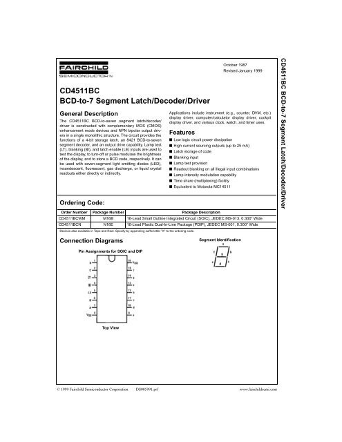
CD4511BC BCD-to-7 Segment Latch/Decoder/Driver - Soemtron.org
CD4511BC BCD-to-7 Segment Latch/Decoder/Driver - Soemtron.org
CD4511BC BCD-to-7 Segment Latch/Decoder/Driver - Soemtron.org
- No tags were found...

You also want an ePaper? Increase the reach of your titles
YUMPU automatically turns print PDFs into web optimized ePapers that Google loves.
<strong>CD4511BC</strong>Truth TableInputsOutputsLE BI LT D C B A a b c d e f g DisplayX X 0 X X X X 1 1 1 1 1 1 1 BX 0 1 X X X X 0 0 0 0 0 0 00 1 1 0 0 0 0 1 1 1 1 1 1 0 00 1 1 0 0 0 1 0 1 1 0 0 0 0 10 1 1 0 0 1 0 1 1 0 1 1 0 1 20 1 1 0 0 1 1 1 1 1 1 0 0 1 30 1 1 0 1 0 0 0 1 1 0 0 1 1 40 1 1 0 1 0 1 1 0 1 1 0 1 1 50 1 1 0 1 1 0 0 0 1 1 1 1 1 60 1 1 0 1 1 1 1 1 1 0 0 0 0 70 1 1 1 0 0 0 1 1 1 1 1 1 1 80 1 1 1 0 0 1 1 1 1 0 0 1 1 90 1 1 1 0 1 0 0 0 0 0 0 0 00 1 1 1 0 1 1 0 0 0 0 0 0 00 1 1 1 1 0 0 0 0 0 0 0 0 00 1 1 1 1 0 1 0 0 0 0 0 0 00 1 1 1 1 1 0 0 0 0 0 0 0 00 1 1 1 1 1 1 0 0 0 0 0 0 01 1 1 X X X X * *X = Don’t Care*Depends upon the <strong>BCD</strong> code applied during the 0 <strong>to</strong> 1 transition of LE.Displaywww.fairchildsemi.com 2
Absolute Maximum Ratings(Note 1)DC Supply Voltage (V DD ) −0.5V <strong>to</strong> +18VInput Voltage (V IN )−0.5V <strong>to</strong> V DD +0.5VS<strong>to</strong>rage Temperature Range (T S ) −65°C <strong>to</strong> +150°CPower Dissipation (P D )Dual-In-Line700 mWSmall Outline500 mWLead Temperature (T L )(Soldering, 10 seconds) 260°CRecommended OperatingConditionsDC Supply Voltage (V DD )Input Voltage (V IN )Operating Temperature Range (T A )Note 1: Devices should not be connected with power on.3V <strong>to</strong> 15V0V <strong>to</strong> V DD−40°C <strong>to</strong> +85°C<strong>CD4511BC</strong>DC Electrical CharacteristicsSymbol Parameter Conditions−40°C +25°C +85°CMin Max Min Typ Max Min MaxI DD Quiescent V DD = 5V 20 20 150 µASupply Current V DD = 10V 40 40 300 µAV DD = 15V 80 80 600 µAV OL Output Voltage V DD = 5V 0.01 0 0.01 0.05 VLogical “0” V DD = 10V 0.01 0 0.01 0.05 VLevel V DD = 15V 0.01 0 0.01 0.05 VV OH Output Voltage V DD = 5V 4.1 4.1 4.57 4.1 VLogical “1” V DD = 10V 9.1 9.1 9.58 9.1 VLevel V DD = 15V 14.1 14.1 14.59 14.1 VV IL LOW Level V DD = 5V, V OUT = 3.8V or 0.5V 1.5 2 1.5 1.5 VInput Voltage V DD = 10V, V OUT = 8.8V or 1.0V 3.0 4 3.0 3.0 VV DD = 15V, V OUT = 13.8V or 1.5V 4.0 6 4.0 4.0 VV IH HIGH Level V DD = 5V, V OUT = 0.5V or 3.8V 3.5 3.5 3 3.5 VInput Voltage V DD = 10V, V OUT = 1.0V or 8.8V 7.0 7.0 6 7.0 VV DD = 15V, V OUT = 1.5V or 13.8V 11.0 11.0 9 11.0 VV OH Output V DD = 5V, I OH = 0 mA 4.1 4.1 4.57 4.1 V(Source) Drive V DD = 5V, I OH = 5 mA 4.24 VVoltage V DD = 5V, I OH = 10 mA 3.6 3.6 4.12 3.3 VV DD = 5V, I OH = 15 mA 3.94 VV DD = 5V, I OH = 20 mA 2.8 2.8 3.75 2.5 VV DD = 5V, I OH = 25 mA 3.54 VV DD = 10V, I OH = 0 mA 9.1 9.1 9.58 9.1 VV DD = 10V, I OH = 5 mA 9.26 VV DD = 10V, I OH = 10 mA 8.75 8.75 9.17 8.45 VV DD = 10V, I OH = 15 mA 9.04 VV DD = 10V, I OH = 20 mA 8.1 8.1 8.9 7.8 VV DD = 10V, I OH = 25 mA 8.75 VV DD = 15V, I OH = 0 mA 14.1 14.1 14.59 14.1 VV DD = 15V, I OH = 5 mA 14.27 VV DD = 15V, I OH = 10 mA 13.75 13.75 14.18 13.45 VV DD = 15V, I OH = 15 mA 14.07 VV DD = 15V, I OH = 20 mA 13.1 13.1 13.95 12.8 VV DD = 15V, I OH = 25 mA 13.8 VI OL LOW Level V DD = 5V, V OL = 0.4V 0.52 0.44 0.88 0.36 mAOutput Current V DD = 10V, V OL = 0.5V 1.3 1.1 2.25 0.9 mAV DD = 15V, V OL = 1.5V 3.6 3.0 8.8 2.4 mAI IN Input Current V DD = 15V, V IN = 0V −0.30 −10 −5 −0.30 −1.0 µAV DD = 15V, V IN = 15V 0.30 10 −5 0.30 1.0 µAUnits3 www.fairchildsemi.com
<strong>CD4511BC</strong>AC Electrical Characteristics (Note 2)T A = 25°C and C L = 50 pF, typical temperature coefficient for all values of V DD = 0.3%/°CSymbol Parameter Conditions Min Typ Max UnitsC IN Input Capacitance V IN = 0 5.0 7.5 pFt r Output Rise Time V DD = 5V 40 80 ns(Figure 1a) V DD = 10V 30 60 nsNote 2: AC Parameters are guaranteed by DC correlated testing.V DD = 15V 25 50 nst f Output Fall Time V DD = 5V 125 250 ns(Figure 1a) V DD = 10V 75 150 nsV DD = 15V 65 130 nst PLH Turn-Off Delay Time V DD = 5V 640 1280 ns(Data) (Figure 1a) V DD = 10V 250 500 nsV DD = 15V 175 350 nst PHL Turn-On Delay Time V DD = 5V 720 1440 ns(Data) (Figure 1a) V DD = 10V 290 580 nsV DD = 15V 195 400 nst PLH Turn-Off Delay Time V DD = 5V 320 640 ns(Blank) (Figure 1a) V DD = 10V 130 260 nsV DD = 15V 100 200 nst PHL Turn-On Delay Time V DD = 5V 485 970 ns(Blank) (Figure 1a) V DD = 10V 200 400 nsV DD = 15V 160 320 nst PLH Turn-Off Delay Time V DD = 5V 313 625 ns(Lamp Test) (Figure 1a) V DD = 10V 125 250 nsV DD = 15V 90 180 nst PHL Turn-On Delay Time V DD = 5V 313 625 ns(Lamp Test) (Figure 1 a) V DD = 10V 125 250 nsV DD = 15V 90 180 nst SETUP Setup Time V DD = 5V 180 90 ns(Figure 1b) V DD = 10V 76 38 nsV DD = 15V 40 20 nst HOLD Hold Time V DD = 5V 0 −90 ns(Figure 1b) V DD = 10V 0 −38 nsV DD = 15V 0 −20 nsPW LE Minimum <strong>Latch</strong> Enable V DD = 5V 520 260 nsPulse Width (Figure 1 c) V DD = 10V 220 110 nsV DD = 15V 130 65 nswww.fairchildsemi.com 4
Switching Time Waveforms<strong>CD4511BC</strong>FIGURE 1.5 www.fairchildsemi.com
<strong>CD4511BC</strong>Typical ApplicationsLight Emitting Diode (LED) ReadoutGas Discharge ReadoutLiquid Crystal (LC) ReadoutDirect DC drive of LC’s not recommended for life of LC readouts.Incandescent ReadoutFluorescent Readout**A filament pre-warm resis<strong>to</strong>r is recommended <strong>to</strong> reduce filament thermalshock and increase the effective cold resistance of the filament.www.fairchildsemi.com 6
Physical Dimensions inches (millimeters) unless otherwise noted<strong>CD4511BC</strong>16-Lead Small Outline Integrated Circuit (SOIC), JEDEC MS-013, 0.300” WidePackage Number M16B7 www.fairchildsemi.com
<strong>CD4511BC</strong> <strong>BCD</strong>-<strong>to</strong>-7 <strong>Segment</strong> <strong>Latch</strong>/<strong>Decoder</strong>/<strong>Driver</strong>Physical Dimensions inches (millimeters) unless otherwise noted (Continued)16-Lead Plastic Dual-In-Line Package (PDIP), JEDEC MS-001, 0.300” WidePackage Number N16ELIFE SUPPORT POLICYFAIRCHILD’S PRODUCTS ARE NOT AUTHORIZED FOR USE AS CRITICAL COMPONENTS IN LIFE SUPPORTDEVICES OR SYSTEMS WITHOUT THE EXPRESS WRITTEN APPROVAL OF THE PRESIDENT OF FAIRCHILDSEMICONDUCTOR CORPORATION. As used herein:1. Life support devices or systems are devices or systemswhich, (a) are intended for surgical implant in<strong>to</strong> thebody, or (b) support or sustain life, and (c) whose failure<strong>to</strong> perform when properly used in accordance withinstructions for use provided in the labeling, can be reasonablyexpected <strong>to</strong> result in a significant injury <strong>to</strong> theuser.2. A critical component in any component of a life supportdevice or system whose failure <strong>to</strong> perform can be reasonablyexpected <strong>to</strong> cause the failure of the life supportdevice or system, or <strong>to</strong> affect its safety or effectiveness.www.fairchildsemi.comFairchild does not assume any responsibility for use of any circuitry described, no circuit patent licenses are implied and Fairchild reserves the right at any time without notice <strong>to</strong> change said circuitry and specifications.