PRECISION 1A REGULATORS - Soemtron.org
PRECISION 1A REGULATORS - Soemtron.org
PRECISION 1A REGULATORS - Soemtron.org

You also want an ePaper? Increase the reach of your titles
YUMPU automatically turns print PDFs into web optimized ePapers that Google loves.
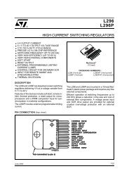
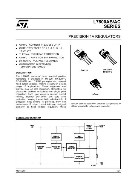
L7800AB/ACSERIES<strong>PRECISION</strong> <strong>1A</strong> <strong>REGULATORS</strong>■OUTPUT CURRENT IN EXCESS OF <strong>1A</strong>■ OUTPUT VOLTAGES OF 5; 6; 8; 9; 12; 15;18; 20; 24V■ THERMAL OVERLOAD PROTECTION■ OUTPUT TRANSITION SOA PROTECTION■ 2% OUTPUT VOLTAGE TOLERANCE■ GUARANTEED IN EXTENDEDTEMPERATURE RANGEDESCRIPTIONThe L7800A series of three terminal positiveregulators is available in TO-220, TO-220FP,TO-220FM and D 2 PAK packages and severalfixed output voltages, making it useful in a widerange of applications. These regulators canprovide local on-card regulation, eliminating thedistribution problem associated with single pointregulation. Each type employs internal currentlimiting, thermal shut-down and safe areaprotection, making it essentially indestructible. Ifadequate heat sinking is provided, they candeliver over <strong>1A</strong> output current, Although designedprimarily as fixed voltage regulators, theseTO-220D 2 PAKTO-220FPTO-220FMdevices can be used with external components toobtain adjustable voltage and currents.SCHEMATIC DIAGRAMMarch 20041/21
L7800AB/AC SERIESABSOLUTE MAXIMUM RATINGSSymbol Parameter Value UnitV IDC Input Voltage (for V O =5to18V)(for V O = 20, 24V)I O Output Current Internally Limited mAP D Power Dissipation Internally Limited mWT stg Storage Temperature Range -65 to +150 °CTOperating Junction Temperature Range (for L7800AC)0to+150°Cop(for L7800AB)-40 to +125°CAbsolute Maximum Ratings are those values beyond which damage to the device may occur. Functional operation under these condition isnot implied.3540VVTHERMAL DATASymbol Parameter TO-220 TO-220FP TO-220FM D 2 PAK UnitR thj-case Thermal Resistance Junction-case 3 5 5 3 °C/WR thj-amb Thermal Resistance Junction-ambient 50 60 60 62.5 °C/WSHEMATIC DIAGRAM2/21
L7800AB/AC SERIESCONNECTION DIAGRAM (top view)TO-220 (Any Type)TO-220FP/TO-220FMD 2 PAKORDERING CODESTYPE TO-220 TO-220FP TO-220FM(*) Available in Tape & Reel with the suffix "-TR".D 2 PAK(A Type) (*)D 2 PAK(C Type) (T & R)OUTPUTVOLTAGEL7805AB L7805ABV L7805ABP L7805ABF L7805ABD2T 5 VL7805AC L7805ACV L7805ACP L7805ACF L7805ACD2T L7805AC-D2TR 5 VL7806AB L7806ABV L7806ABP L7806ABF L7806ABD2T 6 VL7806AC L7806ACV L7806ACP L7806ACF L7806ACD2T 6 VL7808AB L7808ABV L7808ABP L7808ABF L7808ABD2T 8 VL7808AC L7808ACV L7808ACP L7808ACF L7808ACD2T 8 VL7809AB L7809ABV L7809ABP L7809ABF L7809ABD2T 9 VL7809AC L7809ACV L7809ACP L7809ACF L7809ACD2T 9 VL7812AB L7812ABV L7812ABP L7812ABF L7812ABD2T 12 VL7812AC L7812ACV L7812ACP L7812ACF L7812ACD2T 12 VL7815AB L7815ABV L7815ABP L7815ABF L7815ABD2T 15 VL7815AC L7815ACV L7815ACP L7815ACF L7815ACD2T 15 VL7818AB L7818ABV L7818ABP L7818ABF L7818ABD2T 18 VL7818AC L7818ACV L7818ACP L7818ACF L7818ACD2T 18 VL7820AB L7820ABV L7820ABP L7820ABF L7820ABD2T 20 VL7820AC L7820ACV L7820ACP L7820ACF L7820ACD2T 20 VL7824AB L7824ABV L7824ABP L7824ABF L7824ABD2T 24 VL7824AC L7824ACV L7824ACP L7824ACF L7824ACD2T 24 VAPPLICATION CIRCUITS3/21
L7800AB/AC SERIESTEST CIRCUITSFigure 1 : DC ParameterFigure 2 : Load RegulationFigure 3 : Ripple Rejection4/21
L7800AB/AC SERIESELECTRICAL CHARACTERISTICS OF L7805A (V I =10V, I O =<strong>1A</strong>, T J = 0 to 150°C (L7805AC),T J = -40 to 125°C (L7805AB), unless otherwise specified.)Symbol Parameter Test Conditions Min. Typ. Max. UnitV O Output Voltage T J = 25°C 4.9 5 5.1 VV O Output Voltage I O =5mAto<strong>1A</strong> P O ≤ 15W4.8 5 5.2 VV I = 7.5 to 20V∆V O (*) Line Regulation V I = 7.5 to 25V I O = 500 mA 7 50 mVV I =8to12V 10 50 mVV I =8to12V T J = 25°C 2 25 mVV I = 7.3 to 20V T J = 25°C 7 50 mV∆V O (*) Load Regulation I O = 5mA to <strong>1A</strong> 25 100 mVI O =5mAto1.5A T J = 25°C 30 100 VI O = 250 to 750mA 8 50 VI q Quiescent Current T J = 25°C 4.3 6 mA6 mA∆I q Quiescent Current Change V I =8to25V I O = 500 mA 0.8 mAV I = 7.5 to 20V T J = 25°C 0.8 mAI O =5mAto<strong>1A</strong> 0.5 mASVR Supply Voltage Rejection V I = 8 to 18V f = 120Hz68 dBI O = 500mAV d Dropout Voltage I O =<strong>1A</strong> T J = 25°C 2 VeN Output Noise Voltage T A = 25°C B =10Hz to 100KHz 10 µV/V OR O Output Resistance f =1KHz 17 mΩI sc Short Circuit Current V I = 35V T A =25°C 0.2 AI scp Short Circuit Peak Current T J = 25°C 2.2 A∆V O /∆T Output Voltage Drift -1.1 mv/°C(*) Load and Line Regulation are specified at constant junction temperature. Changes in V O due to heating effects must be taken into accountseparately. Pulse testing with low duty cycle is used.5/21
L7800AB/AC SERIESELECTRICAL CHARACTERISTICS OF L7806A (V I =11V, I O =<strong>1A</strong>, T J = 0 to 150°C (L7806AC),T J = -40 to 125°C (L7806AB), unless otherwise specified.)Symbol Parameter Test Conditions Min. Typ. Max. UnitV O Output Voltage T J = 25°C 5.88 6 6.12 VV O Output Voltage I O =5mAto<strong>1A</strong> P O ≤ 15W5.76 6 6.24 VV I = 8.6 to 21V∆V O (*) Line Regulation V I = 8.6 to 25V I O = 500 mA 9 60 mVV I =9to13V 11 60 mVV I =9to13V T J = 25°C 3 30 mVV I = 8.3 to 21V T J = 25°C 9 60 mV∆V O (*) Load Regulation I O = 5mA to <strong>1A</strong> 25 100 mVI O =5mAto1.5A T J = 25°C 30 100 VI O = 250 to 750mA 10 50 VI q Quiescent Current T J = 25°C 4.3 6 mA6 mA∆I q Quiescent Current Change V I =9to25V I O = 500 mA 0.8 mAV I = 8.6 to 21V T J = 25°C 0.8 mAI O =5mAto<strong>1A</strong> 0.5 mASVR Supply Voltage Rejection V I = 9 to 19V f = 120Hz65 dBI O = 500mAV d Dropout Voltage I O =<strong>1A</strong> T J = 25°C 2 VeN Output Noise Voltage T A = 25°C B =10Hz to 100KHz 10 µV/V OR O Output Resistance f =1KHz 17 mΩI sc Short Circuit Current V I = 35V T A =25°C 0.2 AI scp Short Circuit Peak Current T J = 25°C 2.2 A∆V O /∆T Output Voltage Drift -0.8 mV/°C(*) Load and Line Regulation are specified at constant junction temperature. Changes in V O due to heating effects must be taken into accountseparately. Pulse testing with low duty cycle is used.6/21
L7800AB/AC SERIESELECTRICAL CHARACTERISTICS OF L7808A (V I =14V, I O =<strong>1A</strong>, T J = 0 to 150°C (L7808AC),T J = -40 to 125°C (L7808AB), unless otherwise specified.)Symbol Parameter Test Conditions Min. Typ. Max. UnitV O Output Voltage T J = 25°C 7.84 8 8.16 VV O Output Voltage I O =5mAto<strong>1A</strong> P O ≤ 15W7.7 8 8.3 VV I =10.6 to 23V∆V O (*) Line Regulation V I = 10.6 to 25V I O = 500 mA 12 80 mVV I = 11 to 17V 15 80 mVV I =11to17V T J = 25°C 5 40 mVV I = 10.4 to 23V T J = 25°C 12 80 mV∆V O (*) Load Regulation I O = 5mA to <strong>1A</strong> 25 100 mVI O =5mAto1.5A T J = 25°C 30 100 VI O = 250 to 750mA 10 50 VI q Quiescent Current T J = 25°C 4.3 6 mA6 mA∆I q Quiescent Current Change V I =11to25V I O = 500 mA 0.8 mAV I = 10.6 to 23V T J = 25°C 0.8 mAI O =5mAto<strong>1A</strong> 0.5 mASVR Supply Voltage Rejection V I = 11.5 to 21.5V f = 120Hz62 dBI O = 500mAV d Dropout Voltage I O =<strong>1A</strong> T J = 25°C 2 VeN Output Noise Voltage T A = 25°C B =10Hz to 100KHz 10 µV/V OR O Output Resistance f =1KHz 18 mΩI sc Short Circuit Current V I = 35V T A =25°C 0.2 AI scp Short Circuit Peak Current T J = 25°C 2.2 A∆V O /∆T Output Voltage Drift -0.8 mV/°C(*) Load and Line Regulation are specified at constant junction temperature. Changes in V O due to heating effects must be taken into accountseparately. Pulse testing with low duty cycle is used.7/21
L7800AB/AC SERIESELECTRICAL CHARACTERISTICS OF L7809A (V I =15V, I O =<strong>1A</strong>, T J = 0 to 150°C (L7809AC),T J = -40 to 125°C (L7809AB), unless otherwise specified.)Symbol Parameter Test Conditions Min. Typ. Max. UnitV O Output Voltage T J = 25°C 8.82 9 9.18 VV O Output Voltage I O =5mAto<strong>1A</strong> P O ≤ 15W8.65 9 9.35 VV I =10.6 to 23V∆V O (*) Line Regulation V I = 10.6 to 25V I O = 500 mA 12 90 mVV I = 11 to 17V 15 90 mVV I =11to17V T J = 25°C 5 45 mVV I = 10.4 to 23V T J = 25°C 12 90 mV∆V O (*) Load Regulation I O = 5mA to <strong>1A</strong> 25 100 mVI O =5mAto1.5A T J = 25°C 30 100 VI O = 250 to 750mA 10 50 VI q Quiescent Current T J = 25°C 4.3 6 mA6 mA∆I q Quiescent Current Change V I =11to25V I O = 500 mA 0.8 mAV I = 10.6 to 23V T J = 25°C 0.8 mAI O =5mAto<strong>1A</strong> 0.5 mASVR Supply Voltage Rejection V I = 11.5 to 21.5V f = 120Hz61 dBI O = 500mAV d Dropout Voltage I O =<strong>1A</strong> T J = 25°C 2 VeN Output Noise Voltage T A = 25°C B =10Hz to 100KHz 10 µV/V OR O Output Resistance f =1KHz 18 mΩI sc Short Circuit Current V I = 35V T A =25°C 0.2 AI scp Short Circuit Peak Current T J = 25°C 2.2 A∆V O /∆T Output Voltage Drift -0.8 mV/°C(*) Load and Line Regulation are specified at constant junction temperature. Changes in V O due to heating effects must be taken into accountseparately. Pulse testing with low duty cycle is used.8/21
L7800AB/AC SERIESELECTRICAL CHARACTERISTICS OF L7812A (V I =19V, I O =<strong>1A</strong>, T J = 0 to 150°C (L7812AC),T J = -40 to 125°C (L7812AB), unless otherwise specified.)Symbol Parameter Test Conditions Min. Typ. Max. UnitV O Output Voltage T J = 25°C 11.75 12 12.25 VV O Output Voltage I O =5mAto<strong>1A</strong> P O ≤ 15W11.5 12 12.5 VV I =14.8 to 27V∆V O (*) Line Regulation V I = 14.8 to 30V I O = 500 mA 13 120 mVV I = 16 to 22V 16 120 mVV I = 16 to 22V T J = 25°C 6 60 mVV I = 14.5 to 27V T J = 25°C 13 120 mV∆V O (*) Load Regulation I O = 5mA to <strong>1A</strong> 25 100 mVI O =5mAto1.5A T J = 25°C 30 100 VI O = 250 to 750mA 10 50 VI q Quiescent Current T J = 25°C 4.4 6 mA6 mA∆I q Quiescent Current Change V I = 15 to 30V I O = 500 mA 0.8 mAV I = 14.8 to 27V T J = 25°C 0.8 mAI O =5mAto<strong>1A</strong> 0.5 mASVR Supply Voltage Rejection V I = 15 to 25V f = 120Hz60 dBI O = 500mAV d Dropout Voltage I O =<strong>1A</strong> T J = 25°C 2 VeN Output Noise Voltage T A = 25°C B =10Hz to 100KHz 10 µV/V OR O Output Resistance f =1KHz 18 mΩI sc Short Circuit Current V I = 35V T A =25°C 0.2 AI scp Short Circuit Peak Current T J = 25°C 2.2 A∆V O /∆T Output Voltage Drift -1 mV/°C(*) Load and Line Regulation are specified at constant junction temperature. Changes in V O due to heating effects must be taken into accountseparately. Pulse testing with low duty cycle is used.9/21
L7800AB/AC SERIESELECTRICAL CHARACTERISTICS OF L7815A (V I =23V, I O =<strong>1A</strong>, T J = 0 to 150°C (L7815AC),T J = -40 to 125°C (L7815AB), unless otherwise specified.)Symbol Parameter Test Conditions Min. Typ. Max. UnitV O Output Voltage T J = 25°C 14.7 15 15.3 VV O Output Voltage I O =5mAto<strong>1A</strong> P O ≤ 15W14.4 15 15.6 VV I = 17.9 to 30V∆V O (*) Line Regulation V I = 17.9 to 30V I O = 500 mA 13 150 mVV I = 20 to 26V 16 150 mVV I = 20 to 26V T J = 25°C 6 75 mVV I = 17.5 to 30V T J = 25°C 13 150 mV∆V O (*) Load Regulation I O = 5mA to <strong>1A</strong> 25 100 mVI O =5mAto1.5A T J = 25°C 30 100 VI O = 250 to 750mA 10 50 VI q Quiescent Current T J = 25°C 4.4 6 mA6 mA∆I q Quiescent Current Change V I = 17.5 to 30V I O = 500 mA 0.8 mAV I = 17.5 to 30V T J = 25°C 0.8 mAI O =5mAto<strong>1A</strong> 0.5 mASVR Supply Voltage Rejection V I = 18.5 to 28.5V f = 120Hz58 dBI O = 500mAV d Dropout Voltage I O =<strong>1A</strong> T J = 25°C 2 VeN Output Noise Voltage T A = 25°C B =10Hz to 100KHz 10 µV/V OR O Output Resistance f =1KHz 19 mΩI sc Short Circuit Current V I = 35V T A =25°C 0.2 AI scp Short Circuit Peak Current T J = 25°C 2.2 A∆V O /∆T Output Voltage Drift -1 mV/°C(*) Load and Line Regulation are specified at constant junction temperature. Changes in V O due to heating effects must be taken into accountseparately. Pulse testing with low duty cycle is used.10/21
L7800AB/AC SERIESELECTRICAL CHARACTERISTICS OF L7818A (V I =27V, I O =<strong>1A</strong>, T J = 0 to 150°C (L7818AC),T J = -40 to 125°C (L7818AB), unless otherwise specified.)Symbol Parameter Test Conditions Min. Typ. Max. UnitV O Output Voltage T J = 25°C 17.64 18 18.36 VV O Output Voltage I O =5mAto<strong>1A</strong> P O ≤ 15W17.3 18 18.7 VV I = 21 to 33V∆V O (*) Line Regulation V I = 21 to 33V I O = 500 mA 25 180 mVV I = 24 to 30V 28 180 mVV I = 24 to 30V T J = 25°C 10 90 mVV I = 20.6 to 33V T J = 25°C 5 180 mV∆V O (*) Load Regulation I O = 5mA to <strong>1A</strong> 25 100 mVI O =5mAto1.5A T J = 25°C 30 100 VI O = 250 to 750mA 10 50 VI q Quiescent Current T J = 25°C 4.5 6 mA6 mA∆I q Quiescent Current Change V I = 21 to 33V I O = 500 mA 0.8 mAV I = 21 to 33V T J = 25°C 0.8 mAI O =5mAto<strong>1A</strong> 0.5 mASVR Supply Voltage Rejection V I = 22 to 32V f = 120Hz57 dBI O = 500mAV d Dropout Voltage I O =1 A T J = 25°C 2 VeN Output Noise Voltage T A = 25°C B =10Hz to 100KHz 10 µV/V OR O Output Resistance f =1KHz 19 mΩI sc Short Circuit Current V I = 35V T A =25°C 0.2 AI scp Short Circuit Peak Current T J = 25°C 2.2 A∆V O /∆T Output Voltage Drift -1 mV/°C(*) Load and Line Regulation are specified at constant junction temperature. Changes in V O due to heating effects must be taken into accountseparately. Pulse testing with low duty cycle is used.11/21
L7800AB/AC SERIESELECTRICAL CHARACTERISTICS OF L7820A (V I =28V, I O =<strong>1A</strong>, T J = 0 to 150°C (L7820AC),T J = -40 to 125°C (L7820AB), unless otherwise specified.)Symbol Parameter Test Conditions Min. Typ. Max. UnitV O Output Voltage T J = 25°C 19.6 20 20.4 VV O Output Voltage I O =5mAto<strong>1A</strong> P O ≤ 15W19.2 20 20.8 VV I = 23 to 35V∆V O (*) Line Regulation V I = 23 to 35V I O = 500 mA 200 mVV I = 26 to 32V 200 mVV I = 26 to 32V T J = 25°C 100 mVV I = 23 to 32V T J = 25°C 200 mV∆V O (*) Load Regulation I O = 5mA to <strong>1A</strong> 25 100 mVI O =5mAto1.5A T J = 25°C 30 100 VI O = 250 to 750mA 10 50 VI q Quiescent Current T J = 25°C 4.5 6 mA6 mA∆I q Quiescent Current Change V I = 23 to 35V I O = 500 mA 0.8 mAV I = 23 to 35V T J = 25°C 0.8 mAI O =5mAto<strong>1A</strong> 0.5 mASVR Supply Voltage Rejection V I = 24 to 35V f = 120Hz56 dBI O = 500mAV d Dropout Voltage I O =1 A T J = 25°C 2 VeN Output Noise Voltage T A = 25°C B =10Hz to 100KHz 10 µV/V OR O Output Resistance f =1KHz 20 mΩI sc Short Circuit Current V I = 35V T A =25°C 0.2 AI scp Short Circuit Peak Current T J = 25°C 2.2 A∆V O /∆T Output Voltage Drift -1 mV/°C(*) Load and Line Regulation are specified at constant junction temperature. Changes in V O due to heating effects must be taken into accountseparately. Pulse testing with low duty cycle is used.12/21
L7800AB/AC SERIESELECTRICAL CHARACTERISTICS OF L7824A (V I =33V, I O =<strong>1A</strong>, T J = 0 to 150°C (L7824AC),T J = -40 to 125°C (L7824AB), unless otherwise specified.)Symbol Parameter Test Conditions Min. Typ. Max. UnitV O Output Voltage T J = 25°C 23.5 24 24.5 VV O Output Voltage I O =5mAto<strong>1A</strong> P O ≤ 15W23 24 25 VV I = 27.3 to 38V∆V O (*) Line Regulation V I = 27 to 38V I O = 500 mA 31 240 mVV I = 30 to 36V 35 240 mVV I = 30 to 36V T J = 25°C 14 120 mVV I = 26.7 to 38V T J = 25°C 31 240 mV∆V O (*) Load Regulation I O = 5mA to <strong>1A</strong> 25 100 mVI O =5mAto1.5A T J = 25°C 30 100 VI O = 250 to 750mA 10 50 VI q Quiescent Current T J = 25°C 4.6 6 mA6 mA∆I q Quiescent Current Change V I = 27.3 to 38V I O = 500 mA 0.8 mAV I = 27.3 to 38V T J = 25°C 0.8 mAI O =5mAto<strong>1A</strong> 0.5 mASVR Supply Voltage Rejection V I = 28 to 38V f = 120Hz54 dBI O = 500mAV d Dropout Voltage I O =1 A T J = 25°C 2 VeN Output Noise Voltage T A = 25°C B =10Hz to 100KHz 10 µV/V OR O Output Resistance f =1KHz 20 mΩI sc Short Circuit Current V I = 35V T A =25°C 0.2 AI scp Short Circuit Peak Current T J = 25°C 2.2 A∆V O /∆T Output Voltage Drift -1.5 mV/°C(*) Load and Line Regulation are specified at constant junction temperature. Changes in V O due to heating effects must be taken into accountseparately. Pulse testing with low duty cycle is used.13/21
L7800AB/AC SERIESAPPLICATION INFORMATIONDESIGN CONSIDERATIONThe L7800A Series of fixed voltage regulators aredesigned with Thermal Overload Protection thatshuts down the circuit when subjected to anexcessive power overload condition, InternalShort-circuit Protection that limits the maximumcurrent the circuit will pass, and Output transistorSafe-Area Compensation that reduces the outputshort-circuit current as the voltage across the passtransistor is increased. In many low currentapplications, compensation capacitors are notrequired. However, it is recommended that theregulator input be bypassed with capacitor if theregulator is connected to the power supply filterwith long lengths, or if the output load capacitanceis large. An input bypass capacitor should beselected to provide good high frequencycharacteristics to insure stable operation under allload conditions. A 0.33mF or larger tantalum,mylar or other capacitor having low internalimpedance at high frequencies should be chosen.The bypass capacitor should be mounted with theshortest possible leads directly across theregulators input terminals. Normally goodconstruction techniques should be used tominimize ground loops and lead resistance dropssince the regulator has no external sense lead.The addition of an operational amplifier allowsadjustment to higher or intermediate values whileretaining regulation characteristics. The minimumvoltage obtained with the arrangement is 2Vgreater than the regulator voltage.The circuit of figure 6 can be modified to providesupply protection against short circuit by adding ashort circuit sense resistor, RSC, and anadditional PNP transistor. The current sensingPNP must be able to handle the short circuitcurrent of the three terminal regulator Therefore afour ampere plastic power transistor is specified.Figure 5 : DC ParameterV O , 7.0 to 20VV I -V O ≥ 2.0VFigure 6 : DC ParameterVR BEQ11 = ⎯⎯⎯⎯⎯⎯II Q1REQ - ⎯⎯ βQ1VI BEQ1O =I REG +Q 1 (I REG ⎯⎯⎯⎯)R 1Figure 7 : DC ParameterFigure 4 : DC ParameterV xxI O = ⎯⎯ +I dR 114/21
L7800AB/AC SERIESTO-220 MECHANICAL DATADIM.mm.inchMIN. TYP MAX. MIN. TYP. MAX.A 4.40 4.60 0.173 0.181C 1.23 1.32 0.048 0.051D 2.40 2.72 0.094 0.107D1 1.27 0.050E 0.49 0.70 0.019 0.027F 0.61 0.88 0.024 0.034F1 1.14 1.70 0.044 0.067F2 1.14 1.70 0.044 0.067G 4.95 5.15 0.194 0.203G1 2.4 2.7 0.094 0.106H2 10.0 10.40 0.393 0.409L2 16.4 0.645L4 13.0 14.0 0.511 0.551L5 2.65 2.95 0.104 0.116L6 15.25 15.75 0.600 0.620L7 6.2 6.6 0.244 0.260L9 3.5 3.93 0.137 0.154DIA. 3.75 3.85 0.147 0.151P011C15/21
L7800AB/AC SERIESTO-220FP MECHANICAL DATADIM.mm.inchMIN. TYP MAX. MIN. TYP. MAX.A 4.40 4.60 0.173 0.181B 2.5 2.7 0.098 0.106D 2.5 2.75 0.098 0.108E 0.45 0.70 0.017 0.027F 0.75 1 0.030 0.039F1 1.15 1.50 0.045 0.059F2 1.15 1.50 0.045 0.059G 4.95 5.2 0.194 0.204G1 2.4 2.7 0.094 0.106H 10.0 10.40 0.393 0.409L2 16 0.630L3 28.6 30.6 1.126 1.204L4 9.8 10.6 0.385 0.417L6 15.9 16.4 0.626 0.645L7 9 9.3 0.354 0.366DIA. 3 3.2 0.118 0.126EDABL6L7L3¯F1FG1HGL2F2L41 2 37012510/G16/21
L7800AB/AC SERIESTO-220FM MECHANICAL DATADIM.mm.inchMIN. TYP MAX. MIN. TYP. MAX.A 4.50 4.90 0.177 0.193B 3.04 3.44 0.120 0.135D 2.56 2.96 0.101 0.117E 0.45 0.50 0.60 0.018 0.020 0.024F 0.70 0.90 0.028 0.035F1 1.47 0.058G 5.08 0.200G1 2.34 2.54 2.74 0.092 0.100 0.108H 9.96 10.36 0.392 0.408L2 15.8 0.622L4 9.45 10.05 0.372 0.396L6 15.67 16.07 0.617 0.633L7 8.99 9.39 0.354 0.370L8 3.30 0.130DIA. 3.08 3.28 0.121 0.1297012510C/G17/21
L7800AB/AC SERIESD 2 PAK (A TYPE) MECHANICAL DATADIM.mm.inchMIN. TYP MAX. MIN. TYP. MAX.A 4.4 4.6 0.173 0.18<strong>1A</strong>1 0.03 0.23 0.001 0.009b 0.7 0.93 0.027 0.036b2 1.14 1.7 0.044 0.067c 0.45 0.6 0.017 0.023c2 1.23 1.36 0.048 0.053D 8.95 9.35 0.352 0.368D1 8 0.315E 10 10.4 0.393 0.409E1 8.5 0.335e 2.54 0.100e1 4.88 5.28 0.192 0.208H 15 15.85 0.590 0.624J1 2.49 2.69 0.098 0.106L 2.29 2.79 0.090 0.110L1 1.27 1.4 0.050 0.055L2 1.3 1.75 0.051 0.069R 0.4 0.016V2 0° 8° 0° 8°0079457/I18/21
L7800AB/AC SERIESD 2 PAK (C TYPE) MECHANICAL DATADIM.mm.inchMIN. TYP MAX. MIN. TYP. MAX.A 4.3 4.7 0.169 0.185A1 0 0.20 0.000 0.008b 0.70 0.90 0.028 0.035b2 1.17 1.37 0.046 0.054c 0.45 0.50 0.6 0.018 0.020 0.024c2 1.25 1.30 1.40 0.049 0.051 0.055D 9.0 9.2 9.4 0.354 0.362 0.370D1 7.5 0.295E 9.8 10.2 0.386 0.402E1 7.5 0.295e 2.54 0.100e1 5.08 0.200H 15 15.30 15.60 0.591 0.602 0.614J1 2.20 2.60 0.087 0.102L 1.79 2.79 0.070 0.110L1 1.0 1.4 0.039 0.055L2 1.2 1.6 0.047 0.063R 0.3 0.012V2 0° 3° 0° 3°0079457/I19/21
L7800AB/AC SERIESTape & Reel D 2 PAK-P 2 PAK-D 2 PAK/A-P 2 PAK/A MECHANICAL DATADIM.mm.inchMIN. TYP MAX. MIN. TYP. MAX.A 180 7.086C 12.8 13.0 13.2 0.504 0.512 0.519D 20.2 0.795N 60 2.362T 14.4 0.567Ao 10.50 10.6 10.70 0.413 0.417 0.421Bo 15.70 15.80 15.90 0.618 0.622 0.626Ko 4.80 4.90 5.00 0.189 0.193 0.197Po 3.9 4.0 4.1 0.153 0.157 0.161P 11.9 12.0 12.1 0.468 0.472 0.47620/21
L7800AB/AC SERIESInformation furnished is believed to be accurate and reliable. However, STMicroelectronics assumes no responsibility for theconsequences of use of such information nor for any infringement of patents or other rights of third parties which may result fromits use. No license is granted by implication or otherwise under any patent or patent rights of STMicroelectronics. Specificationsmentioned in this publication are subject to change without notice. This publication supersedes and replaces all informationpreviously supplied. STMicroelectronics products are not authorized for use as critical components in life support devices orsystems without express written approval of STMicroelectronics.The ST logo is a registered trademark of STMicroelectronicsAll other names are the property of their respective owners© 2004 STMicroelectronics - All Rights ReservedSTMicroelectronics GROUP OF COMPANIESAustralia - Belgium - Brazil - Canada - China - Czech Republic - Finland - France - Germany - Hong Kong - India - Israel - Italy - Japan -Malaysia - Malta - Morocco - Singapore - Spain - Sweden - Switzerland - United Kingdom - United States.http://www.st.com21/21