SN74LS145 1-of-10 Decoder/Driver Open-Collector - Datasheet ...
SN74LS145 1-of-10 Decoder/Driver Open-Collector - Datasheet ...
SN74LS145 1-of-10 Decoder/Driver Open-Collector - Datasheet ...

Create successful ePaper yourself
Turn your PDF publications into a flip-book with our unique Google optimized e-Paper software.
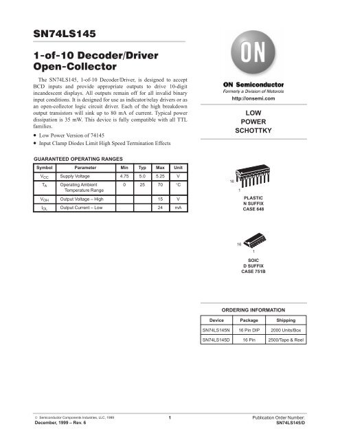
The <strong>SN74LS145</strong>, 1-<strong>of</strong>-<strong>10</strong> <strong>Decoder</strong>/<strong>Driver</strong>, is designed to acceptBCD inputs and provide appropriate outputs to drive <strong>10</strong>-digitincandescent displays. All outputs remain <strong>of</strong>f for all invalid binaryinput conditions. It is designed for use as indicator/relay drivers or asan open-collector logic circuit driver. Each <strong>of</strong> the high breakdownoutput transistors will sink up to 80 mA <strong>of</strong> current. Typical powerdissipation is 35 mW. This device is fully compatible with all TTLfamilies.• Low Power Version <strong>of</strong> 74145• Input Clamp Diodes Limit High Speed Termination Effectshttp://onsemi.comLOWPOWERSCHOTTKYGUARANTEED OPERATING RANGESSymbol Parameter Min Typ Max UnitV CC Supply Voltage 4.75 5.0 5.25 VT AOperating AmbientTemperature Range0 25 70 °CV OH Output Voltage – High 15 VI OL Output Current – Low 24 mA161PLASTICN SUFFIXCASE 648161SOICD SUFFIXCASE 751BORDERING INFORMATIONDevice Package Shipping<strong>SN74LS145</strong>N 16 Pin DIP 2000 Units/Box<strong>SN74LS145</strong>D16 Pin2500/Tape & Reel© Semiconductor Components Industries, LLC, 1999December, 1999 – Rev. 61 Publication Order Number:<strong>SN74LS145</strong>/D
<strong>SN74LS145</strong>CONNECTION DIAGRAM DIP (TOP VIEW)V CC P 0 P 1 P 2 P 3 Q 9 Q 8 Q 7Q 0 Q 1 Q 2 Q 3 Q 4 Q 5 Q 6 GND16 15 14 13 12 11 <strong>10</strong> 91 2 3 4 5 6 7 8LOADING(Note a)PIN NAMESHIGHLOWP 0 , P 1 , P 2 , P 3Q 0 – Q 9BCD InputsOutputs0.5 U.L.<strong>Open</strong> <strong>Collector</strong>0.25 U.L.15 U.L.NOTES:a) 1 TTL Unit Load (U.L.) = 40 A HIGH/1.6 mA LOW.LOGIC SYMBOL15 14 13 12P 0 P 1 P 2 P 3Q 0 Q 1 Q 2 Q 3 Q 4 Q 5 Q 6 Q 7 Q 8 Q 91 2 3 4 5 6 7 9 <strong>10</strong> 11V CC = PIN 16GND = PIN 8http://onsemi.com2
<strong>SN74LS145</strong>LOGIC DIAGRAMINPUTSP 0 P 1 P 2 P 3INPUTINVERTERS0 0 1 1 2 2 3 3DECODE/DRIVERGATESQ 0 Q 1 Q 2 Q 3 Q 4 Q 5 Q 6 Q 7 Q 8 Q 9OUTPUTSINPUTSTRUTH TABLEOUTPUTSP 3 P 2 P 1 P 0 Q 0 Q 1 Q 2 Q 3 Q 4 Q 5 Q 6 Q 7 Q 8 Q 9L L L L L H H H H H H H H HL L L H H L H H H H H H H HL L H L H H L H H H H H H HL L H H H H H L H H H H H HL H L L H H H H L H H H H HL H L H H H H H H L H H H HL H H L H H H H H H L H H HL H H H H H H H H H H L H HH L L L H H H H H H H H L HH L L H H H H H H H H H H LH L H L H H H H H H H H H HH L H H H H H H H H H H H HH H L L H H H H H H H H H HH H L H H H H H H H H H H HH H H L H H H H H H H H H HH H H H H H H H H H H H H HH = HIGH Voltage LevelL = LOW Voltage Levelhttp://onsemi.com3
<strong>SN74LS145</strong>DC CHARACTERISTICS OVER OPERATING TEMPERATURE RANGE (unless otherwise specified)LimitsSymbol Parameter Min Typ Max Unit Test ConditionsV IH Input HIGH Voltage 2.0 VV ILInput LOW Voltage0.8VGuaranteed Input HIGH Voltage forAll InputsGuaranteed Input LOW Voltage forAll InputsV IK Input Clamp Diode Voltage –0.65 –1.5 V V CC = MIN, I IN = – 18 mAI OH Output HIGH Current 250 µA V CC = MIN, V OH = MAX0.25 0.4 V I OL = 12 mAV OL Output LOW Voltage 0.35 0.5 V I OL = 24 mAI IHInput HIGH Current2.3 3.0 V I OL = 80 mA20 µA V CC = MAX, V IN = 2.7 V0.1 mA V CC = MAX, V IN = 7.0 VI IL Input LOW Current –0.4 mA V CC = MAX, V IN = 0.4 VI CC Power Supply Current 13 mA V CC = MAX, V IN = GNDAC CHARACTERISTICS (T A = 25°C)LimitsV CC = V CC MIN,V IN = V IL or V IHper Truth TableSymbol Parameter Min Typ Max Unit Test Conditionst PHLt PLHPropagation DelayP n Input to Q n Output5050nsV CC = 5.0 VC L = 45 pFAC WAVEFORMSV IN1.3 V1.3 VV IN1.3 V1.3 Vt PHLt PLHt PHLt PLHV OUT1.3 V1.3 VV OUT1.3 V1.3 VFigure 1. Figure 2.http://onsemi.com4
<strong>SN74LS145</strong>PACKAGE DIMENSIONSN SUFFIXPLASTIC PACKAGECASE 648–08ISSUE R16–A–1 8HGF9D 16 PLBSCK0.25 (0.0<strong>10</strong>) M TSEATING–T– PLANEAMJLMNOTES:1. DIMENSIONING AND TOLERANCING PER ANSIY14.5M, 1982.2. CONTROLLING DIMENSION: INCH.3. DIMENSION L TO CENTER OF LEADS WHENFORMED PARALLEL.4. DIMENSION B DOES NOT INCLUDE MOLD FLASH.5. ROUNDED CORNERS OPTIONAL.INCHES MILLIMETERSDIM MIN MAX MIN MAXA 0.740 0.770 18.80 19.55B 0.250 0.270 6.35 6.85C 0.145 0.175 3.69 4.44D 0.015 0.021 0.39 0.53F 0.040 0.70 1.02 1.77G 0.<strong>10</strong>0 BSC 2.54 BSCH 0.050 BSC 1.27 BSCJ 0.008 0.015 0.21 0.38K 0.1<strong>10</strong> 0.130 2.80 3.30L 0.295 0.305 7.50 7.74M 0 <strong>10</strong> 0 <strong>10</strong>S 0.020 0.040 0.51 1.01http://onsemi.com5
<strong>SN74LS145</strong>PACKAGE DIMENSIONSD SUFFIXPLASTIC SOIC PACKAGECASE 751B–05ISSUE J–T–SEATINGPLANE16 91 8G–A–K–B–D 16 PL0.25 (0.0<strong>10</strong>) M T B S A SP 8 PL0.25 (0.0<strong>10</strong>) M B SCMR X 45JFNOTES:1. DIMENSIONING AND TOLERANCING PER ANSIY14.5M, 1982.2. CONTROLLING DIMENSION: MILLIMETER.3. DIMENSIONS A AND B DO NOT INCLUDEMOLD PROTRUSION.4. MAXIMUM MOLD PROTRUSION 0.15 (0.006)PER SIDE.5. DIMENSION D DOES NOT INCLUDE DAMBARPROTRUSION. ALLOWABLE DAMBARPROTRUSION SHALL BE 0.127 (0.005) TOTALIN EXCESS OF THE D DIMENSION ATMAXIMUM MATERIAL CONDITION.MILLIMETERS INCHESDIM MIN MAX MIN MAXA 9.80 <strong>10</strong>.00 0.386 0.393B 3.80 4.00 0.150 0.157C 1.35 1.75 0.054 0.068D 0.35 0.49 0.014 0.019F 0.40 1.25 0.016 0.049G 1.27 BSC 0.050 BSCJ 0.19 0.25 0.008 0.009K 0.<strong>10</strong> 0.25 0.004 0.009M 0 7 0 7P 5.80 6.20 0.229 0.244R 0.25 0.50 0.0<strong>10</strong> 0.019http://onsemi.com6
<strong>SN74LS145</strong>Noteshttp://onsemi.com7
<strong>SN74LS145</strong>ON Semiconductor and are trademarks <strong>of</strong> Semiconductor Components Industries, LLC (SCILLC). SCILLC reserves the right to make changeswithout further notice to any products herein. SCILLC makes no warranty, representation or guarantee regarding the suitability <strong>of</strong> its products for any particularpurpose, nor does SCILLC assume any liability arising out <strong>of</strong> the application or use <strong>of</strong> any product or circuit, and specifically disclaims any and all liability,including without limitation special, consequential or incidental damages. “Typical” parameters which may be provided in SCILLC data sheets and/orspecifications can and do vary in different applications and actual performance may vary over time. All operating parameters, including “Typicals” must bevalidated for each customer application by customer’s technical experts. SCILLC does not convey any license under its patent rights nor the rights <strong>of</strong> others.SCILLC products are not designed, intended, or authorized for use as components in systems intended for surgical implant into the body, or other applicationsintended to support or sustain life, or for any other application in which the failure <strong>of</strong> the SCILLC product could create a situation where personal injury ordeath may occur. Should Buyer purchase or use SCILLC products for any such unintended or unauthorized application, Buyer shall indemnify and holdSCILLC and its <strong>of</strong>ficers, employees, subsidiaries, affiliates, and distributors harmless against all claims, costs, damages, and expenses, and reasonableattorney fees arising out <strong>of</strong>, directly or indirectly, any claim <strong>of</strong> personal injury or death associated with such unintended or unauthorized use, even if such claimalleges that SCILLC was negligent regarding the design or manufacture <strong>of</strong> the part. SCILLC is an Equal Opportunity/Affirmative Action Employer.PUBLICATION ORDERING INFORMATIONNorth America Literature Fulfillment:Literature Distribution Center for ON SemiconductorP.O. Box 5163, Denver, Colorado 80217 USAPhone: 303–675–2175 or 800–344–3860 Toll Free USA/CanadaFax: 303–675–2176 or 800–344–3867 Toll Free USA/CanadaEmail: ONlit@hibbertco.comN. American Technical Support: 800–282–9855 Toll Free USA/CanadaEUROPE: LDC for ON Semiconductor – European SupportGerman Phone: (+1) 303–308–7140 (M–F 2:30pm to 5:00pm Munich Time)Email: ONlit–german@hibbertco.comFrench Phone: (+1) 303–308–7141 (M–F 2:30pm to 5:00pm Toulouse Time)Email: ONlit–french@hibbertco.comEnglish Phone: (+1) 303–308–7142 (M–F 1:30pm to 5:00pm UK Time)Email: ONlit@hibbertco.comASIA/PACIFIC: LDC for ON Semiconductor – Asia SupportPhone: 303–675–2121 (Tue–Fri 9:00am to 1:00pm, Hong Kong Time)Toll Free from Hong Kong 800–4422–3781Email: ONlit–asia@hibbertco.comJAPAN: ON Semiconductor, Japan Customer Focus Center4–32–1 Nishi–Gotanda, Shinagawa–ku, Tokyo, Japan 141–8549Phone: 81–3–5487–8345Email: r14153@onsemi.comFax Response Line: 303–675–2167800–344–38<strong>10</strong> Toll Free USA/CanadaON Semiconductor Website: http://onsemi.comFor additional information, please contact your localSales Representative.http://onsemi.com8<strong>SN74LS145</strong>/D
This datasheet has been downloaded from:www.<strong>Datasheet</strong>Catalog.com<strong>Datasheet</strong>s for electronic components.