Micro MATE-N-LOK Connectors - Logic IO
Micro MATE-N-LOK Connectors - Logic IO
Micro MATE-N-LOK Connectors - Logic IO
- No tags were found...
You also want an ePaper? Increase the reach of your titles
YUMPU automatically turns print PDFs into web optimized ePapers that Google loves.
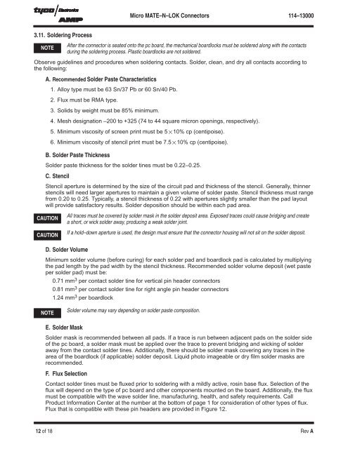
<strong>Micro</strong> <strong>MATE</strong>–N–<strong>LOK</strong> <strong>Connectors</strong>114–130003.11. Soldering ProcessNOTEAfter the connector is seated onto the pc board, the mechanical boardlocks must be soldered along with the contactsduring the soldering process. Plastic boardlocks are not soldered.Observe guidelines and procedures when soldering contacts. Solder, clean, and dry all contacts according tothe following:A. Recommended Solder Paste Characteristics1. Alloy type must be 63 Sn/37 Pb or 60 Sn/40 Pb.2. Flux must be RMA type.3. Solids by weight must be 85% minimum.4. Mesh designation –200 to +325 (74 to 44 square micron openings, respectively).5. Minimum viscosity of screen print must be 5 10% cp (centipoise).6. Minimum viscosity of stencil print must be 7.5 10% cp (centipoise).B. Solder Paste ThicknessSolder paste thickness for the solder tines must be 0.22–0.25.C. StencilStencil aperture is determined by the size of the circuit pad and thickness of the stencil. Generally, thinnerstencils will need larger apertures to maintain a given volume of solder paste. Stencil thickness must rangefrom 0.20 to 0.25. Typically, a stencil thickness of 0.22 with apertures slightly smaller than the pad layoutwill provide satisfactory results. Solder deposition should be within each pad area.CAUT<strong>IO</strong>NCAUT<strong>IO</strong>NAll traces must be covered by solder mask in the solder deposit area. Exposed traces could cause bridging and createa short, or wick solder away, producing a weak solder joint.If a hold–down aperture is used, the design must ensure that the connector housing will not sit on the solder deposit.D. Solder VolumeMinimum solder volume (before curing) for each solder pad and boardlock pad is calculated by multiplyingthe pad length by the pad width by the stencil thickness. Recommended solder volume deposit (wet pasteper solder pad) must be:0.71 mm 3 per contact solder tine for vertical pin header connectors0.81 mm 3 per contact solder tine for right angle pin header connectors1.24 mm 3 per boardlockNOTESolder volume may vary depending on solder paste composition.E. Solder MaskSolder mask is recommended between all pads. If a trace is run between adjacent pads on the solder sideof the pc board, a solder mask must be applied over the trace to prevent bridging and wicking of solderaway from the contact solder tines. Additionally, there should be solder mask covering any traces in thearea of the boardlock (if applicable) solder deposit. Liquid photo imageable or dry film solder masks arerecommended.F. Flux SelectionContact solder tines must be fluxed prior to soldering with a mildly active, rosin base flux. Selection of theflux will depend on the type of pc board and other components mounted on the board. Additionally, the fluxmust be compatible with the wave solder line, manufacturing, health, and safety requirements. CallProduct Information Center at the number at the bottom of page 1 for consideration of other types of flux.Flux that is compatible with these pin headers are provided in Figure 12.12 of 18Rev A


