Micro MATE-N-LOK Connectors - Logic IO
Micro MATE-N-LOK Connectors - Logic IO
Micro MATE-N-LOK Connectors - Logic IO
- No tags were found...

Create successful ePaper yourself
Turn your PDF publications into a flip-book with our unique Google optimized e-Paper software.
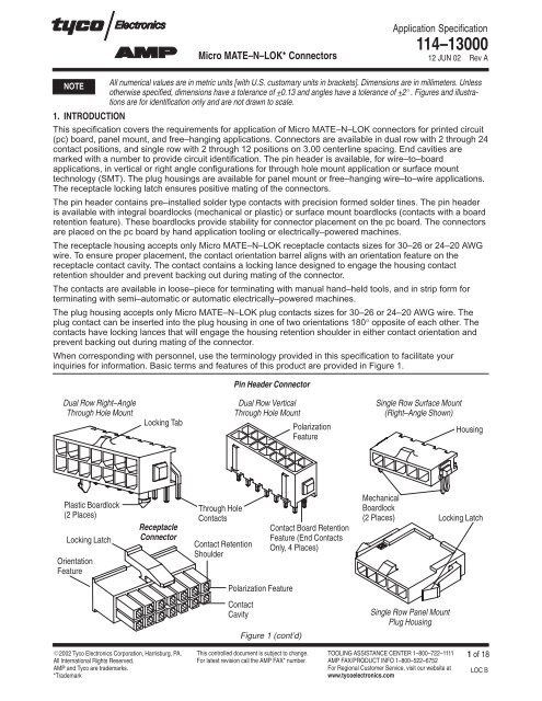
<strong>Micro</strong> <strong>MATE</strong>–N–<strong>LOK</strong>* <strong>Connectors</strong>Application Specification114–1300012 JUN 02 Rev ANOTEAll numerical values are in metric units [with U.S. customary units in brackets]. Dimensions are in millimeters. Unlessotherwise specified, dimensions have a tolerance of +0.13 and angles have a tolerance of +2 . Figures and illustrationsare for identification only and are not drawn to scale.1. INTRODUCT<strong>IO</strong>NThis specification covers the requirements for application of <strong>Micro</strong> <strong>MATE</strong>–N–<strong>LOK</strong> connectors for printed circuit(pc) board, panel mount, and free–hanging applications. <strong>Connectors</strong> are available in dual row with 2 through 24contact positions, and single row with 2 through 12 positions on 3.00 centerline spacing. End cavities aremarked with a number to provide circuit identification. The pin header is available, for wire–to–boardapplications, in vertical or right angle configurations for through hole mount application or surface mounttechnology (SMT). The plug housings are available for panel mount or free–hanging wire–to–wire applications.The receptacle locking latch ensures positive mating of the connectors.The pin header contains pre–installed solder type contacts with precision formed solder tines. The pin headeris available with integral boardlocks (mechanical or plastic) or surface mount boardlocks (contacts with a boardretention feature). These boardlocks provide stability for connector placement on the pc board. The connectorsare placed on the pc board by hand application tooling or electrically–powered machines.The receptacle housing accepts only <strong>Micro</strong> <strong>MATE</strong>–N–<strong>LOK</strong> receptacle contacts sizes for 30–26 or 24–20 AWGwire. To ensure proper placement, the contact orientation barrel aligns with an orientation feature on thereceptacle contact cavity. The contact contains a locking lance designed to engage the housing contactretention shoulder and prevent backing out during mating of the connector.The contacts are available in loose–piece for terminating with manual hand–held tools, and in strip form forterminating with semi–automatic or automatic electrically–powered machines.The plug housing accepts only <strong>Micro</strong> <strong>MATE</strong>–N–<strong>LOK</strong> plug contacts sizes for 30–26 or 24–20 AWG wire. Theplug contact can be inserted into the plug housing in one of two orientations 180° opposite of each other. Thecontacts have locking lances that will engage the housing retention shoulder in either contact orientation andprevent backing out during mating of the connector.When corresponding with personnel, use the terminology provided in this specification to facilitate yourinquiries for information. Basic terms and features of this product are provided in Figure 1.Pin Header ConnectorDual Row Right–AngleThrough Hole MountLocking TabDual Row VerticalThrough Hole MountPolarizationFeatureSingle Row Surface Mount(Right–Angle Shown)HousingPlastic Boardlock(2 Places)Locking LatchOrientationFeatureReceptacleConnectorThrough HoleContactsContact RetentionShoulderContact Board RetentionFeature (End ContactsOnly, 4 Places)MechanicalBoardlock(2 Places)Locking LatchPolarization FeatureContactCavityFigure 1 (cont’d)Single Row Panel MountPlug Housing2002 Tyco Electronics Corporation, Harrisburg, PA.All International Rights Reserved.AMP and Tyco are trademarks.*TrademarkThis controlled document is subject to change.For latest revision call the AMP FAX* number.TOOLING ASSISTANCE CENTER 1–800–722–1111AMP FAX/PRODUCT INFO 1–800–522–6752For Regional Customer Service, visit our website atwww.tycoelectronics.com1 of 18LOC B
<strong>Micro</strong> <strong>MATE</strong>–N–<strong>LOK</strong> <strong>Connectors</strong>114–13000Receptacle ContactPlug ContactRear CutoffTabWire BarrelInsulation BarrelOrientation BarrelLockingLanceBoxWire BarrelInsulation BarrelRear CutoffTabSpring Member(2 Places)Front CutoffTabLockingLanceFigure 1 (end)2. REFERENCE <strong>MATE</strong>RIAL2.1. Revision SummaryThis paragraph is reserved for a revision summary covering the most recent additions and changes made tothis specification which include the following:Per EC 0990–1602–01: Updated document to corporate requirements Added new single row connector information to Section 1 Added new information to Paragraph 2.6 Deleted art and added new art to Figure 1 Added new panel mount information in Paragraph 3.5 and new Figure 2 and renumbered Combined old Figure 2 and table from Figure 3 to make new Figure 3 Added new Paragraph 3.8.B and Figure 8 Deleted old and added new pc board layouts in Figure 11 Changed soldering information in Paragraphs 3.11.B, 3.11.C, and 3.11.D Added agency approvals in Section 4, QUALIFICAT<strong>IO</strong>NS Added new tooling information to Section 5, TOOLING Added new art to Figure 202.2. Customer AssistanceProduct Part Number 794618 and Product Code A309 are representative of <strong>Micro</strong> <strong>MATE</strong>–N–<strong>LOK</strong> connectors.Use of these numbers will identify the product line and expedite your inquiries through a service networkestablished to help you obtain product and tooling information. Such information can be obtained through alocal representative (Field Service Engineer, Field Applications Engineer, etc.) or, after purchase, by calling theProduct Information Center at the number at the bottom of page 1.2.3. DrawingsCustomer Drawings for specific products are available from the service network. The information contained inCustomer Drawings takes priority if there is a conflict with this specification or with any other technicaldocumentation supplied by Tyco Electronics.2.4. ManualsManual 402–40 is available upon request and can be used as a guide to soldering. This manual providesinformation on various flux types and characteristics with the commercial designation and flux removalprocedures. A checklist is included in the manual as a guide for information on soldering problems.2.5. SpecificationsProduct Specification 108–1836 provides product performance and test information.2 of 18Rev A
<strong>Micro</strong> <strong>MATE</strong>–N–<strong>LOK</strong> <strong>Connectors</strong>114–130002.6. Instructional MaterialThe following list includes available instruction sheets (408–series) that provide assembly procedures forproduct, operation, maintenance and repair of tooling, as well as setup and operation procedures ofapplicators; and customer manuals (409–series) that provide setup, operation, and maintenance procedures ofmachines.Document Number Document Title408–3295 Preparing Reel of Contacts for Applicator Tooling408–6927 Design Recommendations for PC Board Support Fixture408–7424 Checking Terminal Crimp Height408–7497 Recommended Procedures for “Crush” Crimp Technique408–8040 Heavy Duty Miniature Quick–Change Applicators (Side–Feed Type)408–8053 Conversion Guide for Miniature Quick Change Applicators408–8059 General Preventive Maintenance for Miniature Quick–Change Applicators408–8547 CERTI–CRIMP II Straight Action Hand Tools408–9816 Handling of Reeled Products408–9453 Extraction Reset Tool 843996–[ ]409–5128 AMP–O–LECTRIC* Model “K” Terminating Machine 565435–5409–5842 AMP–O–LECTRIC Model “G” Terminating Machine 354500–[ ]409–5852 AMPOMATOR* CLS III–G Lead–Making Machine 122500–[ ]409–5866 AMPOMATOR CLS IV Lead–Making Machine 217500–[ ]409–5878 AMPOMATOR CLS IV+ Lead–Making Machine 356500–[ ]409–10016 Entry Level Terminator (ELT) Machine 1338600–[ ]409–10027 Stripping Modules 1490500 and 1490502409–10029 Stripping Modules 1490501 and 14905033. REQUIREMENTS3.1. SafetyDo not stack component packages so high that the shipping containers buckle or deform.3.2. MaterialThe receptacle housings are made of flame–retardant black thermoplastic, and the pin header housings aremade of flame retardant high–temperature black thermoplastic to facilitate the soldering process. Themechanical boardlocks are made of phosphor bronze plated with tin and the plastic boardlocks are made ofplastic. <strong>Micro</strong> <strong>MATE</strong>–N–<strong>LOK</strong> (receptacle) contacts are made of phosphor bronze and the pre–installed soldertype (pin header) contacts are made of brass; both available in duplex 30 gold, 15 gold, or bright tin plating.3.3. StorageA. Ultraviolet LightProlonged exposure to ultraviolet light may deteriorate the chemical composition used in the connectormaterial.B. Shelf LifeThe contacts should remain in the shipping containers until ready for use to prevent deformation to thecontacts. The contacts should be used on a first in, first out basis to avoid storage contamination thatcould adversely affect performance.C. Reeled ContactsWhen using reeled contacts, store coil wound reels horizontally and traverse wound reels vertically.3.4. Chemical ExposureDo not store connectors or contacts near any chemical listed below as they may cause stress corrosioncracking in the connectors or contacts.Alkalies Ammonia Citrates Phosphates Citrates Sulfur CompoundsAmines Carbonates Nitrites Sulfur Nitrites Tartrates3.5. Panel Mount LayoutFigure 2 provides the dimensions required for panel mounting the connectors. The recommended panelthickness is 1.57–2.3.Rev A 3 of 18
<strong>Micro</strong> <strong>MATE</strong>–N–<strong>LOK</strong> <strong>Connectors</strong>114–130004.06 +0.101.98 +0.203.05 +0.103.18 +0.205.51 +0.208.71 +0.207.11 +0.10Dim “B” +0.10Dim “C” +0.05Dim “B” +0.104.21 +0.10Dim “C” +0.05/–0.10NUMBER OFPOSIT<strong>IO</strong>NSPLUG HOUSING – DUAL ROWDIM “B”DIM “C”NUMBER OFPOSIT<strong>IO</strong>NSPLUG HOUSING – SINGLE ROWDIM “B”DIM “C”2 4.20 7.88 2 7.20 10.884 7.20 10.88 3 10.20 13.996 10.20 13.88 4 13.20 16.888 13.20 16.88 5 16.20 19.8810 16.20 19.88 6 19.20 22.8812 19.20 22.88 7 22.20 25.8814 22.20 25.88 8 25.20 28.8816 25.20 28.88 9 28.20 31.8818 28.20 31.88 10 31.20 34.8820 31.20 34.88 11 34.20 37.8822 34.20 37.88 12 37.20 40.8824 37.20 40.88 –––3.6. Wire Selection and PreparationFigure 2The contacts will accept stranded wire sizes 30 through 20 AWG with an insulation diameter range of 0.89 to1.53. Proper strip length is necessary to properly insert the wire into the contact. The strip length of the wire isshown in Figure 3.CAUT<strong>IO</strong>NReasonable care must be taken not to nick, scrape, or cut any strands during the stripping operation.2.90–3.53Wire Strip LengthInsulationCONTACTSIZE30–26 02WIRE SIZE(AWG)30 0.512826ConductorCONTACT WIRE BARREL CRIMPHEIGHT +0.05WIDTHCONTACT INSULAT<strong>IO</strong>NBARREL CRIMP WIDTHAPPLICATOR HAND TOOL APPLICATOR HAND TOOL APPLICATOR HAND TOOL0.56 (Recpt)0.53 (Plug) 0.58 1.07 1.070.61 (Recpt)0.56 (Plug) 1.78 1.7824 0.69 0.7424–202022 0.79 0.74 1.40 1.4020 0.89 0.89Figure 34 of 18Rev A
<strong>Micro</strong> <strong>MATE</strong>–N–<strong>LOK</strong> <strong>Connectors</strong>114–130003.7. Crimp RequirementsCAUT<strong>IO</strong>NWire insulation must NOT be cut or broken during the crimping operation. Reasonable care should be taken to provideundamaged wire terminations.The contact must be crimped to the wire according to instructions packaged with applicable tooling.A. Cutoff Tab and BurrCutoff tabs are the remaining portion of the carrier strip after the contact is cut from the strip. The followingdimensional requirements will ensure proper application for these contacts.1. The front cutoff tab must not extend beyond the contact box and the rear cutoff tab must not extendbeyond the insulation barrel more than the limits shown in Figure 4.2. The burr resulting from the cutoff tab shearing must not exceed the dimension shown in Figure 4.B. Locking LanceThe height of the locking lances must be within the specified limits shown in Figure 4.C. Spring MembersThere must be no damage or distortion to the spring members of the receptacle contacts or the pin end ofthe plug contact. See Figure 4.D. Orientation BarrelThere must be no damage or distortion to the orientation barrel. See Figure 4.E. Wire Barrel CrimpThe crimp applied to the wire barrel portion of the contact is the most compressed area and is most criticalin ensuring optimum electrical and mechanical performance of the crimped contact. The wire barrel mustbe crimped in the “F” crimp where the tips of the wire barrel turn inward and capture the wire strands. Thewire barrel crimp height and width must be within the dimensions provided in Figure 4.F. Effective Crimp LengthEffective crimp length is defined as that portion of the wire barrel, excluding bellmouths, fully formed by thecrimping tool. For optimum crimp effectiveness, the crimp must be within the limits shown in Figure 4.G. Wire Barrel SeamThe seam between the two sides of the wire barrel must be completely closed and there must be noevidence of loose wire strands or wire strands visible in the seam. Refer to Figure 4.H. BellmouthsThe front and rear bellmouths caused by extrusion of the contact material during crimping must be withinthe limits shown in Figure 4.I. Wire Barrel FlashWire barrel flash is the formation that may appear on both sides of the wire barrel as the result of crimping.It must not exceed the dimension provided in Figure 4.J. Insulation Barrel CrimpThe insulation barrel crimp is crimped to form a support for the insulation. The insulation barrel must becrimped in the “F” crimp where the tips of the insulation barrel turn inward and capture the wire insulation.The insulation barrel crimp width must be within the dimension provided in Figure 4.K. Insulation Barrel SeamThe seam between the two sides of the insulation barrel must be completely closed and grasp the wireinsulation. Refer to Figure 4.L. Conductor LocationThe wire insulation and conductor must be visible within the transition area (between the contact insulationbarrel and wire barrel). The insulation must not enter the wire barrel. The wire conductor ends must beflush to or extend slightly beyond the wire barrel to the limit provided in Figure 4.Rev A 5 of 18
<strong>Micro</strong> <strong>MATE</strong>–N–<strong>LOK</strong> <strong>Connectors</strong>114–13000NOTE: Receptacle contact shown, plug contact has same dimensions for crimp requirements.Transition Area (WireInsulation and ConductorsMust Be Visible Here)1.80 Min EffectiveCrimp LengthInsulation Barrel MustGrasp Wire InsulationInsulation Does NotEnter Wire BarrelNo Wire StrandsShows in WireBarrel SeamNo Damage toSpring Members0.13 Min RearBellmouthA0.13 MaxFront Bellmouth0.56–0.69Locking LanceHeight0.25 MaxRear Cutoff Tab (SeeDetail A)Insulation Barrel(“F” Crimp)OrientationBarrelAWire ConductorEnds Flush to orExtends 1.58 (Max)Beyond Wire BarrelWire Barrel CrimpWidth (See Table)Section A–ANo Damage or DistortionPermitted in This Area0.13 MaxBurr Allowance0.11 MaxFront Cutoff Tab(See Detail B)Detail AWire Barrel(“F” Crimp)0.20 Max WireBarrel FlashWire Barrel CrimpHeight (See Table)Detail B0.13 MaxBurr AllowanceNOTE: Locking lance height is different for plug contacts. Refer tothe appropriate customer drawings for specific dimensions.Figure 4NOTEThe developed crimp configurations result from using the specific tooling described in Section 5, TOOLING.M. StraightnessThe force applied during crimping may cause some bending between the wire barrel and the matingportion of the contact. Such deformation is acceptable within the following limits.1. Up and DownThe crimped portion, including cutoff tab and burr, must not be bent beyond the limits shown in Figure 5.2. Side–to–SideThe crimped portion must not be bent from one side to the other beyond the limits shown in Figure 5.6 of 18Rev A
<strong>Micro</strong> <strong>MATE</strong>–N–<strong>LOK</strong> <strong>Connectors</strong>114–130004° Max.Up and Down Alignment4° Max.Datum LineSide–to–Side Alignment4° Max.N. Twist and RollFigure 5There should be no twist or roll of the wire barrel or mating portion of the crimped contact beyond the limitsshown in Figure 6.3 (Max)3 (Max)Mating PortionDatum LineAvoid Twistand RollFigure 63.8. Placement of Crimped ContactsA. Receptacle HousingThe contact orientation barrel must be aligned with the receptacle contact cavity orientation feature(located on the back of the receptacle). The contact must be inserted into the housing contact cavity andsnapped into place. When fully inserted, the contact locking lance will engage the receptacle contactretention shoulder and prevent backing out during mating of the connectors. After inserting contact intohousing, pull back lightly on the wire to ensure contact is fully seated. See Figure 7.NOTEAn insertion tool is not required to insert contacts into receptacles.CAUT<strong>IO</strong>NReceptacle contacts are for use with receptacle housings only. Do not insert receptacle contacts into plug housings.Back of ReceptacleContact CavityOrientation FeatureWireHousingContact OrientationBarrelContact LockingLanceContact CavityFigure 7Rev A 7 of 18
<strong>Micro</strong> <strong>MATE</strong>–N–<strong>LOK</strong> <strong>Connectors</strong>114–13000B. Plug HousingThe plug contact can be aligned in one of two different ways, (180° opposite each other) during insertioninto a plug housing. Either alignment is acceptable and will provide engagement of the lances with thehousing locking shelves and prevent backing out during mating of connectors . After inserting contacts intothe housing, pull back lightly on the wire to ensure the contact is fully seated. See Figure 8.CAUT<strong>IO</strong>NPlug contacts are for use with plug housings only. Do not insert plug contacts into receptacle housings.Plug HousingPlug ContactLocking LanceFigure 83.9. Connector SpacingCare must be used to avoid interference between adjacent connectors and other components. The minimumallowable distance between pin headers to ensure proper mating is provided in Figure 9.3.10. PC BoardA. Material and ThicknessThe pc board material shall be glass epoxy (FR–4 or G–10). The pc board thickness shall be 1.57.NOTEContact the Product Information Center at the number listed at the bottom of page 1 for suitability of other boardmaterials and thicknesses.B. ToleranceMaximum allowable bow of the pc board shall be 0.03 over the length of the pin header.Pin Header6.35 MinAllowable DistancePin HeaderPC BoardFigure 98 of 18Rev A
ÉÉÉÉÉÉÉÉÉÉÉÉÉÉÉÉ<strong>Micro</strong> <strong>MATE</strong>–N–<strong>LOK</strong> <strong>Connectors</strong>114–13000C. Layout for Through Hole Mount <strong>Connectors</strong>1. The pc board and lead wires must be solderable in accordance with Test Specification 109–11.2. The pc board holes for the contact solder tines and boardlocks must be drilled and plated through tospecific dimensions to prevent stubbing during placement of the connector on the pc board and toensure optimum continuity for circuits after soldering. The drilled hole size, plating types, and platingthickness will depend on application requirements. The finished hole size must be as stated to provideunrestricted insertion and ensure adequate application of solder to the solder tines. See Figure 10.3. The contact holes and boardlock holes in the pc board must be precisely located to ensure properplacement and optimum performance of the connector. Design the pc board using the dimensionsprovided in Figure 11.Pad Diameter(As Required)ÉÉÉÉTrace Width(As Required)ÇÇ ÉÉÉÉÇÇ ÉÉÉÉÇÇ ÉÉÉÉÇÇ ÉÉÉÉÉÉÉÇÇ ÉÉÉÉÇÇ ÉÉÉÉÉÉÉÇÇ ÉÉÉÉÇÇ ÉÉÉÉÉÉÉFinished Hole Diameter(After Plating)0.80+0.05ÉÉÉÉ ÇÇÇÇÉÉÉÉÉÉÉÉÉÉÇÇÉÉÉÉÉÇÇ ÉÉÇÇÉÉÉÉÉÉÉDrilled Hole Diameter(As Required)ÉÉÉÉÉÉÇÇÉÉÉÉÉÉÉÉÉÉÉÉContact Solder Tine HoleÉÉÉÉÉÉÉÉÉÉÉBoardlock HoleÉÉÉÉDrilled Hole Diameter(Refer to Specific PC BoardLayout, Figure 11)D. Layout for Surface Mount <strong>Connectors</strong>Figure 101. The pc board pads must be solderable in accordance with EIA–638 (Electronic Industries Alliance).2. The connector boardlock holes on the pc board require precise drilling dimensions and the location ofthe circuit pads to these holes is critical to ensure proper placement and optimum performance of theconnector. Recommended pc board pad pattern, dimensions, and tolerances are shown in Figure 11.NOTEFour representative examples of recommended pc board patterns, dimensions, and tolerances are shown in Figure 11.Consult the customer drawings for specific pc board layouts or part numbers not listed in this document. Componentside shown. See Paragraph 2.3.Rev A 9 of 18
<strong>Micro</strong> <strong>MATE</strong>–N–<strong>LOK</strong> <strong>Connectors</strong>114–13000Dual Row Through HoleVertical Metal Through Hole HolddownsNOTE: Board edge dimensions determined by customerCONNPOSNDIM Y2 4.304 7.306 10.308 13.3010 16.3012 19.3014 22.3016 25.3018 28.3020 31.3022 34.3024 37.30Dual Row SMT Right–AngleSMT HolddownsCONNDIMENS<strong>IO</strong>NPOSN W Z2 7.30 –4 10.30 3.006 13.30 6.008 16.30 9.0010 19.30 12.0012 22.30 15.0014 25.30 18.0016 28.30 21.0018 31.30 24.0020 34.30 27.0022 37.30 30.0024 40.30 33.00NOTE: Board edge dimensions determined by customerFigure 11 (cont’d)10 of 18Rev A
<strong>Micro</strong> <strong>MATE</strong>–N–<strong>LOK</strong> <strong>Connectors</strong>114–13000Single Row SMT VerticalMetal Thru–Hole HolddownsCONNDIMENS<strong>IO</strong>NPOSN V Z2 7.40 3.003 10.40 6.004 13.40 9.005 16.40 12.006 19.40 15.007 22.40 18.008 25.40 21.009 28.40 24.0010 31.40 27.0011 34.40 30.0012 37.40 33.00Single Row Thru–Hole Right–AnglePlastic HolddownsPC Board Layoutfor 2–PositionPC Board Layoutfor 3–PositionCONNDIMENS<strong>IO</strong>NPOSN V ZPC Board Layoutfor 4–Position2 – –3 – –4 4.70 9.005 7.70 12.006 10.70 15.007 13.70 18.008 16.70 21.009 19.70 24.0010 22.70 27.0011 25.70 30.0012 28.70 33.00Figure 11 (end)Rev A 11 of 18
<strong>Micro</strong> <strong>MATE</strong>–N–<strong>LOK</strong> <strong>Connectors</strong>114–130003.11. Soldering ProcessNOTEAfter the connector is seated onto the pc board, the mechanical boardlocks must be soldered along with the contactsduring the soldering process. Plastic boardlocks are not soldered.Observe guidelines and procedures when soldering contacts. Solder, clean, and dry all contacts according tothe following:A. Recommended Solder Paste Characteristics1. Alloy type must be 63 Sn/37 Pb or 60 Sn/40 Pb.2. Flux must be RMA type.3. Solids by weight must be 85% minimum.4. Mesh designation –200 to +325 (74 to 44 square micron openings, respectively).5. Minimum viscosity of screen print must be 5 10% cp (centipoise).6. Minimum viscosity of stencil print must be 7.5 10% cp (centipoise).B. Solder Paste ThicknessSolder paste thickness for the solder tines must be 0.22–0.25.C. StencilStencil aperture is determined by the size of the circuit pad and thickness of the stencil. Generally, thinnerstencils will need larger apertures to maintain a given volume of solder paste. Stencil thickness must rangefrom 0.20 to 0.25. Typically, a stencil thickness of 0.22 with apertures slightly smaller than the pad layoutwill provide satisfactory results. Solder deposition should be within each pad area.CAUT<strong>IO</strong>NCAUT<strong>IO</strong>NAll traces must be covered by solder mask in the solder deposit area. Exposed traces could cause bridging and createa short, or wick solder away, producing a weak solder joint.If a hold–down aperture is used, the design must ensure that the connector housing will not sit on the solder deposit.D. Solder VolumeMinimum solder volume (before curing) for each solder pad and boardlock pad is calculated by multiplyingthe pad length by the pad width by the stencil thickness. Recommended solder volume deposit (wet pasteper solder pad) must be:0.71 mm 3 per contact solder tine for vertical pin header connectors0.81 mm 3 per contact solder tine for right angle pin header connectors1.24 mm 3 per boardlockNOTESolder volume may vary depending on solder paste composition.E. Solder MaskSolder mask is recommended between all pads. If a trace is run between adjacent pads on the solder sideof the pc board, a solder mask must be applied over the trace to prevent bridging and wicking of solderaway from the contact solder tines. Additionally, there should be solder mask covering any traces in thearea of the boardlock (if applicable) solder deposit. Liquid photo imageable or dry film solder masks arerecommended.F. Flux SelectionContact solder tines must be fluxed prior to soldering with a mildly active, rosin base flux. Selection of theflux will depend on the type of pc board and other components mounted on the board. Additionally, the fluxmust be compatible with the wave solder line, manufacturing, health, and safety requirements. CallProduct Information Center at the number at the bottom of page 1 for consideration of other types of flux.Flux that is compatible with these pin headers are provided in Figure 12.12 of 18Rev A
<strong>Micro</strong> <strong>MATE</strong>–N–<strong>LOK</strong> <strong>Connectors</strong>114–13000COMMERCIAL DESIGNAT<strong>IO</strong>NFLUX TYPE ACTIVITY RESIDUEKESTERALPHA RMA Mild Noncorrosive 186 611 Product of Kester Solder Co. Product of Alphametals Inc.Figure 12G. Connector PlacementMachine placement of connectors is recommended due to the inherent difficulty of manual placement offine–pitch connectors and to minimize possible damage that could result from improper handling. The topof vertical pin headers has an adhesive–backed pad to facilitate vacuum pick–up and handling, and rightangle pin headers can be picked up by the housing. To avoid damage, connectors should be picked up bythe machine directly from the connector embossed–tape package.CAUT<strong>IO</strong>NIf connectors are placed on the board manually, the connector should be handled only by the housing to avoiddeformation, contamination, or damage to the contact solder tines and boardlocks.1. Surface Mount <strong>Connectors</strong>Optimally, the contact solder tines should be centered on the pc board circuit pads. However, slightmisalignment is permissible as shown in Figure 13.Contact Solder Tine OverhangUp to 50% is PermissiblePC BoardContact Solder Tine Centered onPC Board Circuit Pad PreferredFigure 132. Through Hole Mount <strong>Connectors</strong>When placing through hole mount connectors on the pc board, make sure that the contact solder tinesare aligned and started into the matching holes before seating the connector onto the pc board.H. TechniqueThe connectors can be soldered using wave, non–focused infrared (IR) reflow soldering, or equivalentsoldering technique. It is recommended using SN60 or SN62 solder for these connectors. Thetemperatures and exposure time must be as specified in Figure 14.SOLDERING PROCESS TEMPERATURE (Max) TIME (Max)Wave 260 C [500 F] 5 SecondsI. CleaningIR 225 C [378 F] 90 SecondsFigure 14After soldering, removal of fluxes, residues, and activators is necessary. Consult with the supplier of thesolder and flux for recommended cleaning solvents. Cleaners must be free of dissolved flux and othercontaminants. The following is a list of common cleaning solvents that will not the affect connectors for thetime and temperature specified. See Figure 15.Rev A 13 of 18
<strong>Micro</strong> <strong>MATE</strong>–N–<strong>LOK</strong> <strong>Connectors</strong>114–13000CAUT<strong>IO</strong>NDANGERNOTEEven when using “no clean” solder paste, it is imperative that the contact interface be kept clean of flux and residue,since it acts as an insulator. Flux may migrate under certain conditions with elevated temperatures and, therefore,cleaning is necessary.Consideration must be given to toxicity and other safety requirements recommended by the solvent manufacturer.Refer to the manufacturer’s Material Safety Data Sheet (MSDS) for characteristics and handling of cleaners. It is notrecommended using Trichloroethylene and Methylene Chloride because of harmful occupational and environmentaleffects. Both are carcinogenic (cancer–causing).If you have a particular solvent that is not listed, contact the Product Information Center at the number at the bottom ofpage 1.NAMECLEANERTYPETIME(Minutes)TEMPERATURES(Maximum)CELSIUSFAHRENHEITAlpha 2110 Aqueous 1 132 270Bioact EC–7 Solvent 5 100 212Butyl Carbitol Solvent 1 Room AmbientIsopropyl Alcohol Solvent 5 100 212Kester 5778 Aqueous 5 100 212Kester 5779 Aqueous 5 100 212Loncoterge 520 Aqueous 5 100 212Loncoterge 530 Aqueous 5 100 212Terpene Solvent Solvent 5 100 212 Product of Fry’s Metals, Inc. Product of Petroferm, Inc. Product of Union Carbide Corp. Product of Litton Systems, Inc.Figure 15J. DryingWhen drying cleaned assemblies, make certain that temperature limitations are not exceeded: –40 to105 C [–68 to 221 F]. Excessive temperatures may cause housing degradation or plating deterioration.3.12. Checking Installed ConnectorAll solder joints should conform to the requirements specified in this document and those specified in thefollowing: Workmanship Specification 101–21 for surface mount connectorsTest Specification 109–11 for through hole mount connectorsSolder must be evenly distributed and not cracked. The connector standoffs must be seated on the pc board,and the housing not exceeding the dimension shown in Figure 16.Surface MountPin Header ConnectorThrough Hole MountPin Header Connector0.13 (Max)Standoff(4 Places)Solder JointPC BoardPC BoardStandoff(2 Places)Solder Joint0.13 (Max)Figure 1614 of 18Rev A
<strong>Micro</strong> <strong>MATE</strong>–N–<strong>LOK</strong> <strong>Connectors</strong>114–130003.13. PolarizationThe design of each contact cavity assures polarization for mating connectors.3.14. Mating <strong>Connectors</strong>CAUT<strong>IO</strong>N<strong>Connectors</strong> should be handled only by the housing to avoid deformation, contamination, or damage to the contactsolder tines.The receptacle has an integral locking latch that should be fully seated and latched to the pin header lockingtab after mating. The locking latch and locking tab ensures positive mating of connectors. The distancebetween mating connectors must be considered when determining location of connectors to ensure full mating.The mated dimension of the receptacle housing to the pin header housing is provided in Figure 17.NOTEReceptacles will mate only with the appropriate pin headers or plug housings; the receptacle and pin header or plughousing must have identical number of circuit positions and rows.17.3 MaxDistanceLocking Latch FullySeated onto Locking TabReceptaclePin Header (Right AngleSurface Mount Shown)PC Board Dimension applies to both through hole and surface mount,and right angle and vertical pin headers when mated.Figure 173.15. Strain Relief and Wire DressIf required, wires can be bundled together and supported with cable ties. Wires must not be stretched orconfined in any way that would restrict the floating action of the contacts. Therefore, the wires must remainperpendicular to the connector and avoid an excessively sharp bend radius. The minimum distance for thecable tie, measured from the wire end of the connector to the cable tie is shown in Figure 18.Cable TieWires76.2 MinDistanceFigure 18Rev A 15 of 18
<strong>Micro</strong> <strong>MATE</strong>–N–<strong>LOK</strong> <strong>Connectors</strong>114–130003.16. RepairDamaged connectors must be removed, discarded, and replaced.1. The connectors must be unmated by releasing the locking latch on the receptacle from the locking tabon the pin header and pulling the receptacle straight out.2. Damaged or worn crimp type contacts may be replaced provided there is sufficient slack, afterrestripping the wire, to insert the new contact into the receptacle. An extraction tool must be used toremove individual contacts from the receptacle.3. Pin headers will require standard de–soldering of all contact solder tines. Individual solder typecontacts cannot be replaced.4. QUALIFICAT<strong>IO</strong>N<strong>Micro</strong> <strong>MATE</strong>–N–<strong>LOK</strong> connectors are Recognized by Underwriters Laboratories Inc. (UL) under File E28476,and Certified by the Canadian Standards Association (CSA) under File LR7189.5. TOOLINGTooling part numbers and instructional material packaged (if available) with the tooling are shown in Figure 19.5.1. Extraction and Lance Reset ToolThe extraction and lance reset tool is designed to remove contacts from the receptacles by releasing thecontact locking lance from the housing without overstressing the contact. This tool can also be used to resetlocking lances that have been deformed.5.2. Hand Crimping ToolThe hand crimping tools accommodate the full wire size range for terminating crimp type contacts. These toolsare designed for prototype and low–volume application of loose piece form contacts.5.3. Robotic EquipmentFor automatic machine placement, a pc board support must be used to prevent bowing of the pc board duringthe placement of contacts and boardlocks on the board. It should have flat surfaces with holes or a channellarge enough and deep enough to receive the contacts and boardlocks. The robotic equipment must have atrue position accuracy tolerance to properly locate the contacts. This includes gripper and fixture tolerances aswell as equipment repeatability. It must use the contact datum surfaces detailed on the customer drawing toensure reliable placement.5.4. Power UnitNOTEModified designs and additional tooling concepts may be available to meet other application requirements. Machineshave been designed for a variety of application requirements. For assistance in setting up prototype and productionline equipment, call the Tooling Assistance Center at the number at the bottom of page 1.A. ApplicatorThe applicators are designed to crimp strip form contacts onto pre–stripped wire, and provides for highvolume, heavy duty production requirements. These applicators accept interchangeable crimping dies andmust be installed onto a power unit.B. Semi–Automatic MachineThe AMP–O–LECTRIC machine is an electrical power unit designed for terminating pre–stripped wires toreel–fed contacts. It is designed to be bench mounted and used for high volume applications.C. Automatic MachineThese power units provide the force required to drive applicators for crimping tape–mounted contacts.They can be set up to automatically measure, cut, strip, and terminate wire. They provide for high volume,heavy duty production requirements. The AMPOMATOR CLS IV+ machine is an electrical power unitdesigned to be floor standing.16 of 18Rev A
<strong>Micro</strong> <strong>MATE</strong>–N–<strong>LOK</strong> <strong>Connectors</strong>114–13000Extraction and LanceReset Tool 843996–6Hand Crimping Tool(See Table)Heavy Duty MiniatureQuick–ChangeApplicators (Side–FeedType) (See Table)PC Board Support(Must Be Custom Made)ELT Machine 1338600–[ ]with Optional StrippingModuleAMP–O–LECTRIC Model “K”Terminator Machine565435–5RoboticEquipmentAMPOMATOR CLSLead–Making Machines122500–[ ]; 217500–[ ];356500–[ ]AMP–O–LECTRIC Model “G”Terminating Machine 354500–[ ]with Optional Stripping ModuleWIRESIZERANGE(AWG)HANDCRIMPINGTOOL30–26 02 91502–124–2020 91501–1AMP–O–LECTRICModel “K”Terminating MachineAPPLICATOR (408–8040) forAMP–O–LECTRICModel “G” and ELTTerminating MachinesAMPOMATORCLSLead–Making Machines680894–2 (Recept) 680894–3 (Recept) 680894–1 (Recept)1385377–2 (Plug) 1385377–3 (Plug) 1385377–1 (Plug)680893–2 (Recept) 680893–3 (Recept) 680893–1 (Recept)1385194–2 (Plug) 1385194–3 (Plug) 1385194–1 (Plug)Processes wire size 26 AWG only.Figure 19Rev A 17 of 18
<strong>Micro</strong> <strong>MATE</strong>–N–<strong>LOK</strong> <strong>Connectors</strong>114–130006. VISUAL AIDFigure 20 shows a typical application of <strong>Micro</strong> <strong>MATE</strong>–N–<strong>LOK</strong> connectors. This illustration should be used byproduction personnel to ensure a correctly applied product. Applications which DO NOT appear correct shouldbe inspected using the information in the preceding pages of this specification and in the instructional materialshipped with the product or tooling.INSULAT<strong>IO</strong>N BARREL (“F” CRIMP)MUST BE FOLDED INWARD ANDGRASP WIRE INSULAT<strong>IO</strong>NWIRE BARREL (“F” CRIMP) MUST BEFOLDED INWARD WITH NO PROTRUDINGOR VISIBLE WIRE STRANDSLOCKING LATCH MUST BEFULLY SEATED ONTOLOCKING TABWIRE INSULAT<strong>IO</strong>NAND CONDUCTORSMUST BE VISIBLE INTRANSIT<strong>IO</strong>N AREASPRING MEMBER MUSTNOT BE DAMAGED ORDISTORTEDCONTACT MUSTBE STRAIGHT ANDNOT DEFORMEDIN ANY WAYORIENTAT<strong>IO</strong>N BARREL MUSTNOT BE DEFORMEDLOCKINGLANCE MUSTNOT BEDEFORMEDCONNECTORSMUST BE FULLY<strong>MATE</strong>DLOCKING LATCH MUST BEFULLY SEATED ONTOLOCKING TABCONTACTS MUST BELOCKED IN PLACEHOUSING MUSTNOT BE CRACKEDOR BROKENCONNECTOR MUST BESEATED ON PC BOARDFIGURE 20.SOLDER FILLET MUST BEFORMED EVENLY AROUNDCONTACT SOLDER TINESAND MECHANICALBOARDLOCKSVISUAL AIDSOLDER TINES MUSTBE CENTERED ONCIRCUIT PADS (SLIGHTMISALIGNMENT ISALLOWED)18 of 18Rev A