Ultra Low Power Stereo Audio Codec (Rev. A
Ultra Low Power Stereo Audio Codec (Rev. A
Ultra Low Power Stereo Audio Codec (Rev. A
- No tags were found...

You also want an ePaper? Increase the reach of your titles
YUMPU automatically turns print PDFs into web optimized ePapers that Google loves.
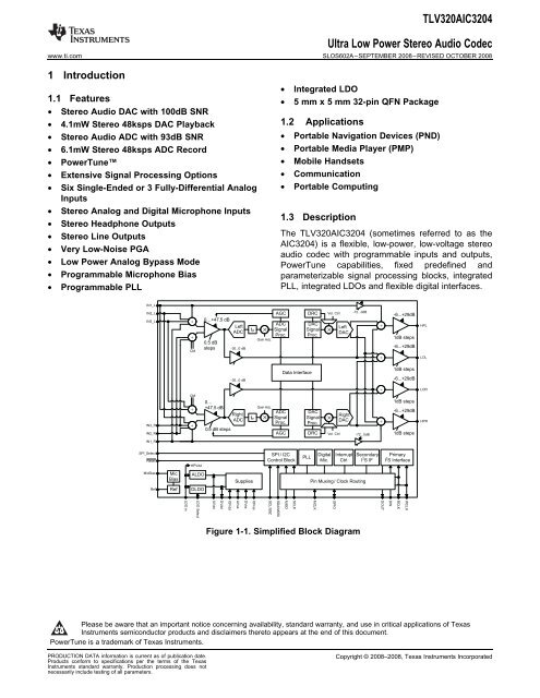
LDO inLDO SelectAVddDVddIOVddAVssDVssIOVssSCL/SSZSDA/MOSIMISOSCLKMCLKGPIODOUTDINBCLKWCLK1 IntroductionTLV320AIC3204<strong>Ultra</strong> <strong>Low</strong> <strong>Power</strong> <strong>Stereo</strong> <strong>Audio</strong> <strong>Codec</strong>www.ti.com SLOS602A–SEPTEMBER 2008–REVISED OCTOBER 2008• Integrated LDO1.1 Features• 5 mm x 5 mm 32-pin QFN Package• <strong>Stereo</strong> <strong>Audio</strong> DAC with 100dB SNR• 4.1mW <strong>Stereo</strong> 48ksps DAC Playback1.2 Applications• <strong>Stereo</strong> <strong>Audio</strong> ADC with 93dB SNR• Portable Navigation Devices (PND)• 6.1mW <strong>Stereo</strong> 48ksps ADC Record• Portable Media Player (PMP)• <strong>Power</strong>Tune• Mobile Handsets• Extensive Signal Processing Options• Communication• Six Single-Ended or 3 Fully-Differential Analog • Portable ComputingInputs• <strong>Stereo</strong> Analog and Digital Microphone Inputs1.3 Description• <strong>Stereo</strong> Headphone Outputs• <strong>Stereo</strong> Line OutputsThe TLV320AIC3204 (sometimes referred to as theAIC3204) is a flexible, low-power, low-voltage stereo• Very <strong>Low</strong>-Noise PGAaudio codec with programmable inputs and outputs,• <strong>Low</strong> <strong>Power</strong> Analog Bypass Mode <strong>Power</strong>Tune capabilities, fixed predefined and• Programmable Microphone Bias parameterizable signal processing blocks, integrated• Programmable PLLPLL, integrated LDOs and flexible digital interfaces.IN1_LIN2_LIN3_LCM0…+47.5 dB0.5 dBstepsLeftADC-30...0 dBtplAGCADC SignalProc.Gain Adj.DRCDACSignalProc.Vol. CtrlLeftDAC-72...0dB-6...+29dB1dB steps-6...+29dBHPLLOL-30...0 dBData Interface1dB steps-6...+29dBLORIN3_RIN2_RCM0…+47.5 dB0.5 dB stepsRightADCtprGain Adj.ADC SignalProc.AGCDACSignalProc.DRCVol. CtrlRightDAC-72...0dB1dB steps-6...+29dB1dB stepsHPRIN1_RSPI_SelectResetHPVddSPI / I2CControl BlockPLLDigitalMic.InterruptCtrlSecondaryI 2 S IFPrimaryI 2 S InterfaceMicBiasMicBiasALDOSuppliesPin Muxing / Clock RoutingRefRefDLDOFigure 1-1. Simplified Block DiagramPlease be aware that an important notice concerning availability, standard warranty, and use in critical applications of TexasInstruments semiconductor products and disclaimers thereto appears at the end of this document.<strong>Power</strong>Tune is a trademark of Texas Instruments.PRODUCTION DATA information is current as of publication date.Products conform to specifications per the terms of the TexasInstruments standard warranty. Production processing does notnecessarily include testing of all parameters.Copyright © 2008–2008, Texas Instruments Incorporated
TLV320AIC3204<strong>Ultra</strong> <strong>Low</strong> <strong>Power</strong> <strong>Stereo</strong> <strong>Audio</strong> <strong>Codec</strong>SLOS602A–SEPTEMBER 2008–REVISED OCTOBER 2008www.ti.com1.4 Detailed DescriptionExtensive Register based control of power, input/output channel configuration, gains, effects,pin-multiplexing and clocks is included, allowing the device to be precisely targeted to its application.Combined with the advanced <strong>Power</strong>Tune technology, the device can cover operations from 8 kHz monovoice playback to audio stereo 192kHz DAC playback, making it ideal for portable battery-powered audioand telephony applications.The record path of the TLV320AIC3204 covers operations from 8kHz mono to 192kHz stereo recording,and contains programmable input channel configurations covering single-ended and differential setups, aswell as floating or mixing input signals. It also includes a digitally-controlled stereo microphone preamplifierand integrated microphone bias. Digital signal processing blocks can remove audible noise that may beintroduced by mechanical coupling, e.g. optical zooming in a digital camera.The playback path offers signal-processing blocks for filtering and effects, and supports flexible mixing ofDAC and analog input signals as well as programmable volume controls. The playback path contains twohigh-power output drivers as well as two fully-differential outputs. The high-power outputs can beconfigured in multiple ways, including stereo and mono BTL.The integrated <strong>Power</strong>Tune technology allows the device to be tuned to just the right power-performancetrade-off. Mobile applications frequently have multiple use cases requiring very low power operation whilebeing used in a mobile environment. When used in a docked environment power consumption typically isless of a concern, while minimizing noise is important. With <strong>Power</strong>Tune, the TLV320AIC3204 addressesboth cases.The voltage supply range for the TLV320AIC3204 for analog is 1.5V–1.95V, and for digital it is1.26V–1.95V. To ease system-level design, LDOs are integrated to generate the appropriate analog ordigital supply from input voltages ranging from 1.8V to 3.6V. Digital I/O voltages are supported in therange of 1.1V–3.6V.The required internal clock of the TLV320AIC3204 can be derived from multiple sources, including theMCLK pin, the BCLK pin, the GPIO pin or the output of the internal PLL, where the input to the PLL againcan be derived from the MCLK pin, the BCLK or GPIO pins. Although using the PLL ensures theavailability of a suitable clock signal, it is not recommended for the lowest power settings. The PLL ishighly programmable and can accept available input clocks in the range of 512kHz to 50MHz.The device is available in the 5-mm × 5-mm, 32-pin QFN package.2 IntroductionSubmit Documentation Feedback
LORLOLIN3_RIN3_LMICBIASREFTLV320AIC3204<strong>Ultra</strong> <strong>Low</strong> <strong>Power</strong> <strong>Stereo</strong> <strong>Audio</strong> <strong>Codec</strong>www.ti.com SLOS602A–SEPTEMBER 2008–REVISED OCTOBER 2008These devices have limited built-in ESD protection. The leads should be shorted together or the device placed inconductive foam during storage or handling to prevent electrostatic damage to the MOS gates.2 Package and Signal Descriptions2.1 Packaging/Ordering InformationPRODUCT PACKAGE PACKAGE OPERATING ORDERING TRANSPORT MEDIA,DESIGNATOR TEMPERATURE NUMBER QUANTITYRANGETLV320AIC3204 QFN RHB –40°C to 85°C TLV320AIC3204IRHBT Tape and Reel, 250TLV320AIC3204IRHBR Tape and Reel, 30002.2 Pin AssignmentsMCLK (1)BCLKWCLKDIN/MFP1DOUT/MFP2OVIDDIOVSSSCLK/MFP31 8GPIO/MFP5 (32)329SCL/SSZRESETSDA/MOSILDO_SELECTMISO/MFP4DV DDSPI_SELECTDV SSIN1_LHPRIN1_RLDOININ2_LHPL2516IN2_R2417AV DDAVSSFigure 2-1. QFN (RHB) Package, Bottom ViewSubmit Documentation Feedback Package and Signal Descriptions 3
TLV320AIC3204<strong>Ultra</strong> <strong>Low</strong> <strong>Power</strong> <strong>Stereo</strong> <strong>Audio</strong> <strong>Codec</strong>SLOS602A–SEPTEMBER 2008–REVISED OCTOBER 2008www.ti.comTERMINAL NAME TYPE DESCRIPTION1 MCLK I Master Clock InputTable 2-1. TERMINAL FUNCTIONS2 BCLK IO <strong>Audio</strong> serial data bus (primary) bit clock3 WCLK IO <strong>Audio</strong> serial data bus (primary) word clock4 DIN I Primary functionMFP15 DOUT O PrimaryMFP2<strong>Audio</strong> serial data bus data inputSecondary function<strong>Audio</strong> serial data bus (secondary) bit clock input<strong>Audio</strong> serial data bus (secondary) word clock inputDigital Microphone InputClock InputGeneral Purpose InputSecondary<strong>Audio</strong> serial data bus data output6 IOVDD <strong>Power</strong> I/O voltage supply 1.1V – 3.6V7 IOVSS Ground I/O ground supply8 SCLK I Primary (SPI_Select = 1)General Purpose OutputClock OutputINT1 OutputINT2 Output<strong>Audio</strong> serial data bus (secondary) bit clock output<strong>Audio</strong> serial data bus (secondary) word clock outputSPI serial clockMFP3 Secondary: (SPI_Select = 0)Headset-detect inputDigital microphone input<strong>Audio</strong> serial data bus (secondary) bit clock input<strong>Audio</strong> serial data bus (secondary) DAC/common word clock input<strong>Audio</strong> serial data bus (secondary) ADC word clock input<strong>Audio</strong> serial data bus (secondary) data inputGeneral Purpose Input9 SCL/ I I 2 C interface serial clock (SPI_Select = 0)SSZ SPI interface mode chip-select signal (SPI_Select = 1)10 SDA/ MOSI I I 2 C interface mode serial data input (SPI_Select = 0)SPI interface mode serial data input (SPI_Select = 1)11 MISO O Primary (SPI_Select = 1)Serial data outputMFP4 Secondary (SPI_Select = 0)General purpose outputCLKOUT outputINT1 outputINT2 output<strong>Audio</strong> serial data bus (primary) ADC word clock outputDigital microphone clock output<strong>Audio</strong> serial data bus (secondary) data output<strong>Audio</strong> serial data bus (secondary) bit clock output<strong>Audio</strong> serial data bus (secondary) word clock output12 SPI_ SELECT I Control mode select pin ( 1 = SPI, 0 = I 2 C )4 Package and Signal DescriptionsSubmit Documentation Feedback
TLV320AIC3204<strong>Ultra</strong> <strong>Low</strong> <strong>Power</strong> <strong>Stereo</strong> <strong>Audio</strong> <strong>Codec</strong>www.ti.com SLOS602A–SEPTEMBER 2008–REVISED OCTOBER 2008TERMINAL NAME TYPE DESCRIPTIONTable 2-1. TERMINAL FUNCTIONS (continued)13 IN1_L I Multifunction Analog Input,or Single-ended configuration: MIC 1 or Line 1 leftor Differential configuration: MIC or Line right, negative14 IN1_R I Multifunction Analog Input,or Single-ended configuration: MIC 1 or Line 1 rightor Differential configuration: MIC or Line right, positive15 IN2_L I Multifunction Analog Input,or Single-ended configuration: MIC 2 or Line 2 rightor Differential configuration: MIC or Line left, positive16 IN2_R I Multifunction Analog Input,or Single-ended configuration: MIC 2 or Line 2 rightor Differential configuration: MIC or Line left, negative17 AVss Ground Analog ground supply18 REF O Reference voltage output for filtering19 MICBIAS O Microphone bias voltage output20 IN3_L I Multifunction Analog Input,or Single-ended configuration: MIC3 or Line 3 left,or Differential configuration: MIC or Line left, positive,or Differential configuration: MIC or Line right, negative21 IN3_R I Multifunction Analog Input,or Single-ended configuration: MIC3 or Line 3 right,or Differential configuration: MIC or Line left, negative,or Differential configuration: MIC or Line right, positive22 LOL O Left line output23 LOR O Right line output24 AVdd <strong>Power</strong> Analog voltage supply 1.5V–1.95VInput when A-LDO disabled,Filtering output when A-LDO enabled25 HPL O Left high power output driver26 LDOIN/ HPVDD <strong>Power</strong> LDO Input supply and Headphone <strong>Power</strong> supply 1.9V– 3.6V27 HPR O Right high power output driver28 DVss Ground Digital Ground and Chip-substrate29 DVdd <strong>Power</strong> If LDO_SELECT Pin = 0 (D-LDO disabled)30 LDO_ SELECT I connect to DVss.31 RESET I Reset (active low)32 GPIO I PrimaryMFP5Digital voltage supply 1.26V – 1.95VIf LDO_SELECT Pin = 1 (D-LDO enabled)SecondaryDigital voltage supply filtering outputGeneral Purpose digital IOCLKOUT OutputINT1 OutputINT2 Output<strong>Audio</strong> serial data bus ADC word clock output<strong>Audio</strong> serial data bus (secondary) bit clock output<strong>Audio</strong> serial data bus (secondary) word clock outputDigital microphone clock outputSubmit Documentation Feedback Package and Signal Descriptions 5
TLV320AIC3204<strong>Ultra</strong> <strong>Low</strong> <strong>Power</strong> <strong>Stereo</strong> <strong>Audio</strong> <strong>Codec</strong>SLOS602A–SEPTEMBER 2008–REVISED OCTOBER 2008www.ti.com3 Electrical Specifications3.1 ABSOLUTE MAXIMUM RATINGSover operating free-air temperature range (unless otherwise noted) (1) VALUE UNITAVdd to AVss –0.3 to 2.2 VDVdd to DVss –0.3 to 2.2 VIOVDD to IOVSS –0.3 to 3.9 VLDOIN to AVss –0.3 to 3.9 VDigital Input voltage to ground –0.3 to IOVDD + 0.3 VAnalog input voltage to ground –0.3 to AVdd + 0.3 VOperating temperature range –40 to 85 °CStorage temperature range –55 to 125 °CJunction temperature (T J Max) 105 °C<strong>Power</strong> dissipation (with thermal pad soldered to board) (T J Max – TA)/ θ JA Wθ JA Thermal impedance 35 C/WLead Temperature Infrared (15 sec) 260 °C(1) Stresses beyond those listed under “absolute maximum ratings” may cause permanent damage to the device. These are stress ratingsonly, and functional operation of the device at these or any other conditions beyond those indicated under “recommended operatingconditions” is not implied. Exposure to absolute-maximum-rated conditions for extended periods may affect device reliability.3.2 RECOMMENDED OPERATING CONDITIONSMIN NOM MAX UNITLDOIN <strong>Power</strong> Supply Voltage Range Referenced to AVss (1) 1.9 3.6 VAVdd 1.5 1.8 1.95 VIOVDD Referenced to IOVSS (1) 1.1 3.6 VDVdd (2) Referenced to DVss (1) 1.26 1.8 1.95 VPLL Input Frequency Clock divider uses fractional divide 10 20 MHz(D > 0), P=1, D Vdd ≥ 1.65V (Refer toTable 5-23)Clock divider uses integer divide 0.512 20 MHz(D = 0), P=1, D Vdd ≥ 1.65V (Refer toTable 5-23)MCLK Master Clock Frequency MCLK; Master Clock Frequency; 50 MHzD Vdd ≥ 1.65VMCLK; Master Clock Frequency; 25D Vdd ≥ 1.26VSCL SCL Clock Frequency 400 kHzLOL, LOR <strong>Stereo</strong> line output load resistance 0.6 10 kΩHPL, HPR <strong>Stereo</strong> headphone output load resistance Single-ended configuration 14.4 16 ΩHeadphone output load resistance Differential configuration 24.4 32 ΩC Lout Digital output load capacitance 10 pFTOPR Operating Temperature Range –40 85 °C(1) All grounds on board are tied together, so they should not differ in voltage by more than 0.2V max, for any combination of groundsignals.(2) At DVdd values lower than 1.65V, the PLL does not function. Please see Table 5-23 for details on maximum clock frequencies.6 Electrical SpecificationsSubmit Documentation Feedback
3.3 ELECTRICAL CHARACTERISTICSTLV320AIC3204<strong>Ultra</strong> <strong>Low</strong> <strong>Power</strong> <strong>Stereo</strong> <strong>Audio</strong> <strong>Codec</strong>www.ti.com SLOS602A–SEPTEMBER 2008–REVISED OCTOBER 2008At 25°C, AVdd, DVdd, IOVDD = +1.8V, LDO_in = 3.3V, AVdd LDO disabled, f s (<strong>Audio</strong>) = 48kHz, Cref = 10 µF on REF PIN,PLL disabled unless otherwise noted.(1) (2)AUDIO ADCPARAMETER TEST CONDITIONS MIN TYP MAX UNITInput signal level (0dB) Single-ended, CM = 0.9V 0.5 V RMS1kHz sine wave inputSingle-ended ConfigurationIN1R to Right ADC and IN1L to Left ADC,R in = 20K, f s = 48kHz,Device Setup AOSR = 128, MCLK = 256*f s ,PLL Disabled; AGC = OFF,Channel Gain = 0dB,Processing Block = PRB_R1,<strong>Power</strong> Tune = PTM_R4Inputs ac-shorted to ground 80 93SNR Signal-to-noise ratio, A-weighted (1) (2) IN2R, IN3R routed to Right ADC and ac-shorted to 93grounddBIN2L, IN3L routed to Left ADC and ac-shorted togroundDR Dynamic range A-weighted (1) (2) –60dB full-scale, 1-kHz input signal 92 dBTHD+NAUDIO ADCTotal Harmonic Distortion plus Noise–3 dB full-scale, 1-kHz input signal –85 –70 dBIN2R,IN3R routed to Right ADC –85IN2L, IN3L routed to Left ADC–3dB full-scale, 1-kHz input signalInput signal level (0dB) Single-ended, CM=0.75V, AVdd = 1.5V 0.375 V RMSDevice Setup1kHz sine wave inputSingle-ended ConfigurationIN1R, IN2R, IN3R routed to Right ADCIN1L, IN2L, IN3L routed to Left ADCR in = 20K, f s = 48kHz,AOSR=128, MCLK = 256* f s ,PLL Disabled, AGC = OFF,Channel Gain = 0dB,Processing Block = PRB_R1<strong>Power</strong> Tune = PTM_R4SNR Signal-to-noise ratio, A-weighted (1) (2) Inputs ac-shorted to ground 91 dBDR Dynamic range A-weighted (1) (2) –60dB full-scale, 1-kHz input signal 90 dBTHD+N Total Harmonic Distortion plus Noise –3dB full-scale, 1-kHz input signal –80 dBAUDIO ADCInput signal level (0dB) Differential Input, CM=0.9V 10 mVDevice Setup1kHz sine wave inputDifferential configurationIN1L and IN1R routed to Right ADCIN2L and IN2R routed to Left ADCR in =10K, f s =48kHz, AOSR=128MCLK = 256* f s PLL DisabledAGC = OFF, Channel Gain=40dB Processing Block= PRB_R1,<strong>Power</strong> Tune = PTM_R4ICN Idle-Channel Noise, A-weighted (1) (2) Inputs ac-shorted to ground, input referred noise 2 µV RMS(1) Ratio of output level with 1-kHz full-scale sine wave input, to the output level with the inputs short circuited, measured A-weighted over a20-Hz to 20-kHz bandwidth using an audio analyzer.(2) All performance measurements done with 20-kHz low-pass filter and, where noted, A-weighted filter. Failure to use such a filter mayresult in higher THD+N and lower SNR and dynamic range readings than shown in the Electrical Characteristics. The low-pass filterremoves out-of-band noise, which, although not audible, may affect dynamic specification valuesSubmit Documentation Feedback Electrical Specifications 7
TLV320AIC3204<strong>Ultra</strong> <strong>Low</strong> <strong>Power</strong> <strong>Stereo</strong> <strong>Audio</strong> <strong>Codec</strong>SLOS602A–SEPTEMBER 2008–REVISED OCTOBER 2008www.ti.comELECTRICAL CHARACTERISTICS (continued)At 25°C, AVdd, DVdd, IOVDD = +1.8V, LDO_in = 3.3V, AVdd LDO disabled, f s (<strong>Audio</strong>) = 48kHz, Cref = 10 µF on REF PIN,PLL disabled unless otherwise noted.AUDIO ADCGain ErrorPARAMETER TEST CONDITIONS MIN TYP MAX UNITInput Channel SeparationInput Pin CrosstalkPSRRADC programmable gain amplifier gain1kHz sine wave input –0.05 dBSingle-ended configurationR in = 20K f s = 48kHz, AOSR=128,MCLK = 256* f s , PLL DisabledAGC = OFF, Channel Gain=0dBProcessing Block = PRB_R1,<strong>Power</strong> Tune = PTM_R4, CM=0.9V1kHz sine wave input at -3dBFS 108 dBSingle-ended configurationIN1L routed to Left ADCIN1R routed to Right ADC, R in = 20KAGC = OFF, AOSR = 128,Channel Gain=0dB, CM=0.9V1kHz sine wave input at –3dBFS on IN2L, IN2L 115 dBinternally not routed.IN1L routed to Left ADCac-coupled to ground1kHz sine wave input at –3dBFS on IN2R,IN2R internally not routed.IN1R routed to Right ADCac-coupled to groundSingle-ended configuration R in = 20K,AOSR=128 Channel, Gain=0dB, CM=0.9V217Hz, 100mVpp signal on AVdd, 55 dBSingle-ended configuration, Rin=20K,Channel Gain=0dB; CM=0.9VSingle-Ended, Rin = 10K, PGA gain set to 0dB 0 dBSingle-Ended, Rin = 10K, PGA gain set to 47.5dB 47.5 dBSingle-Ended, Rin = 20K, PGA gain set to 0dB –6 dBSingle-Ended, Rin = 20K, PGA gain set to 47.5dB 41.5 dBSingle-Ended, Rin = 40K, PGA gain set to 0dB –12 dBSingle-Ended, Rin = 40K, PGA gain set to 47.5dB 35.5 dBADC programmable gain amplifier step size 1-kHz tone 0.5 dB8 Electrical SpecificationsSubmit Documentation Feedback
TLV320AIC3204<strong>Ultra</strong> <strong>Low</strong> <strong>Power</strong> <strong>Stereo</strong> <strong>Audio</strong> <strong>Codec</strong>www.ti.com SLOS602A–SEPTEMBER 2008–REVISED OCTOBER 2008ELECTRICAL CHARACTERISTICS (continued)At 25°C, AVdd, DVdd, IOVDD = +1.8V, LDO_in = 3.3V, AVdd LDO disabled, f s (<strong>Audio</strong>) = 48kHz, Cref = 10 µF on REF PIN,PLL disabled unless otherwise noted.PARAMETER TEST CONDITIONS MIN TYP MAX UNITANALOG BYPASS TO HEADPHONE AMPLIFIER, DIRECT MODEDevice SetupLoad = 16Ω (single-ended), 50pF;Input and Output CM=0.9V;Headphone Output on LDOIN Supply;IN1L routed to HPL and IN1R routed to HPR;Channel Gain=0dBGain Error –0.8 dBNoise, A-weighted (1) Idle Channel, IN1L and IN1R ac-shorted to ground 3 µV RMSTHD Total Harmonic Distortion 446mVrms, 1-kHz input signal –89 dBANALOG BYPASS TO LINE-OUT AMPLIFIER, PGA MODEDevice SetupMICROPHONE BIASLoad = 10KOhm (single-ended), 56pF;Input and Output CM=0.9V;LINE Output on LDOIN Supply;IN1L routed to ADCPGA_L and IN1R routed toADCPGA_R; Rin = 20kADCPGA_L routed to LOL and ADCPGA_R routedto LOR; Channel Gain = 0dBGain Error 0.6 dBIdle Channel, 7 µV RMSIN1L and IN1R ac-shorted to groundNoise, A-weighted (1) Channel Gain=40dB, 3.4 µV RMSInput Signal (0dB) = 5mV rmsInputs ac-shorted to ground, Input ReferredBias voltage Bias voltage CM=0.9V, LDOin = 3.3VMicbias Mode 0, Connect to AVdd or LDOin 1.25 VMicbias Mode 1, Connect to LDOin 1.7 VMicbias Mode 2, Connect to LDOin 2.5 VMicbias Mode 3, Connect to AVdd AVdd VMicbias Mode 3, Connect to LDOin LDOin VCM=0.75V, LDOin = 3.3VMicbias Mode 0, Connect to AVdd or LDOin 1.04 VMicbias Mode 1, Connect to AVdd or LDOin 1.425 VMicbias Mode 2, Connect to LDOin 2.075 VMicbias Mode 3, Connect to AVdd AVdd VMicbias Mode 3, Connect to LDOin LDOin VOutput Noise CM=0.9V, Micbias Mode 2, A-weighted, 20Hz to 1020kHz bandwidth,Current load = 0mA.Current Sourcing Micbias Mode 2, Connect to LDOin 3 mAInline ResistanceMicbias Mode 3, Connect to AVdd 140Micbias Mode 3, Connect to LDOin 87(1) All performance measurements done with 20-kHz low-pass filter and, where noted, A-weighted filter. Failure to use such a filter mayresult in higher THD+N and lower SNR and dynamic range readings than shown in the Electrical Characteristics. The low-pass filterremoves out-of-band noise, which, although not audible, may affect dynamic specification valuesµV RMSΩSubmit Documentation Feedback Electrical Specifications 9
TLV320AIC3204<strong>Ultra</strong> <strong>Low</strong> <strong>Power</strong> <strong>Stereo</strong> <strong>Audio</strong> <strong>Codec</strong>SLOS602A–SEPTEMBER 2008–REVISED OCTOBER 2008www.ti.comELECTRICAL CHARACTERISTICS (continued)At 25°C, AVdd, DVdd, IOVDD = +1.8V, LDO_in = 3.3V, AVdd LDO disabled, f s (<strong>Audio</strong>) = 48kHz, Cref = 10 µF on REF PIN,PLL disabled unless otherwise noted.PARAMETER TEST CONDITIONS MIN TYP MAX UNITAUDIO DAC – STEREO SINGLE-ENDED LINE OUTPUTLoad = 10 kΩ (single-ended), 56pFLine Output on AVdd SupplyInput & Output CM=0.9VDevice Setup DOSR = 128, MCLK=256* f s ,Channel Gain = 0dB, word length = 16 bits,Processing Block = PRB_P1,<strong>Power</strong> Tune = PTM_P3Full scale output voltage (0dB) 0.5 V RMSSNR Signal-to-noise ratio A-weighted (1) (2) All zeros fed to DAC input 87 100 dBDR Dynamic range, A-weighted (1) (2) –60dB 1kHz input full-scale signal, Word length=20 100 dBbitsTHD+N Total Harmonic Distortion plus Noise –3dB full-scale, 1-kHz input signal –83 –70 dBDAC Gain Error 0 dB, 1kHz input full scale signal 0.3 dBDAC Mute Attenuation Mute 119 dBDAC channel separation –1 dB, 1kHz signal, between left and right HP out 113 dBDAC PSRRAUDIO DAC – STEREO SINGLE-ENDED LINE OUTPUTDevice Setup100mVpp, 1kHz signal applied to AVdd 73 dB100mVpp, 217Hz signal applied to AVdd 77 dBLoad = 10 kΩ (single-ended), 56pFLine Output on AVdd SupplyInput & Output CM=0.75V; AVdd=1.5VDOSR = 128MCLK=256* fsChannel Gain = –2dBword length = 20-bitsProcessing Block = PRB_P1<strong>Power</strong> Tune = PTM_P4Full scale output voltage (0dB) 0.375 V RMSSNR Signal-to-noise ratio, A-weighted (1) (2) All zeros fed to DAC input 99 dBDR Dynamic range, A-weighted (1) (2) –60dB 1 kHz input full-scale signal 97 dBTHD+N Total Harmonic Distortion plus Noise –1 dB full-scale, 1-kHz input signal –85 dBAUDIO DAC – STEREO SINGLE-ENDED HEADPHONE OUTPUTDevice SetupLoad = 16Ω (single-ended), 50pFHeadphone Output on AVdd Supply,Input & Output CM=0.9V, DOSR = 128,MCLK=256* f s , Channel Gain=0dBword length = 16 bits;Processing Block = PRB_P1<strong>Power</strong> Tune = PTM_P3Full scale output voltage (0dB) 0.5 V RMSSNR Signal-to-noise ratio, A-weighted (1) (2) All zeros fed to DAC input 87 100 dBDR Dynamic range, A-weighted (1) (2) –60dB 1kHz input full-scale signal, Word Length = 99 dB20 bits, <strong>Power</strong> Tune = PTM_P4THD+N Total Harmonic Distortion plus Noise –3dB full-scale, 1-kHz input signal –83 –70 dBDAC Gain Error 0dB, 1kHz input full scale signal –0.3 dBDAC Mute Attenuation Mute 122 dBDAC channel separation –1dB, 1kHz signal, between left and right HP out 110 dBDAC PSRR100mVpp, 1kHz signal applied to AVdd 73 dB100mVpp, 217Hz signal applied to AVdd 78 dB(1) Ratio of output level with 1-kHz full-scale sine wave input, to the output level with the inputs short circuited, measured A-weighted over a20-Hz to 20-kHz bandwidth using an audio analyzer.(2) All performance measurements done with 20-kHz low-pass filter and, where noted, A-weighted filter. Failure to use such a filter mayresult in higher THD+N and lower SNR and dynamic range readings than shown in the Electrical Characteristics. The low-pass filterremoves out-of-band noise, which, although not audible, may affect dynamic specification values10 Electrical SpecificationsSubmit Documentation Feedback
TLV320AIC3204<strong>Ultra</strong> <strong>Low</strong> <strong>Power</strong> <strong>Stereo</strong> <strong>Audio</strong> <strong>Codec</strong>www.ti.com SLOS602A–SEPTEMBER 2008–REVISED OCTOBER 2008ELECTRICAL CHARACTERISTICS (continued)At 25°C, AVdd, DVdd, IOVDD = +1.8V, LDO_in = 3.3V, AVdd LDO disabled, f s (<strong>Audio</strong>) = 48kHz, Cref = 10 µF on REF PIN,PLL disabled unless otherwise noted.PARAMETER TEST CONDITIONS MIN TYP MAX UNIT<strong>Power</strong> DeliveredAUDIO DAC – STEREO SINGLE-ENDED HEADPHONE OUTPUTR L =16Ω, Output Stage on AVdd = 1.8V 15THDN < 1%, Input CM=0.9V,Output CM=0.9VR L =16 Ω Output Stage on LDOIN = 3.3V, 64THDN < 1% Input CM=0.9V,Output CM=1.65VLoad = 16Ω (single-ended), 50pF,Headphone Output on AVdd Supply,Input & Output CM=0.75V; AVdd=1.5V,Device Setup DOSR = 128, MCLK=256* f s ,Channel Gain = –2dB, word length=20-bits;Processing Block = PRB_P1,<strong>Power</strong> Tune = PTM_P4mWFull scale output voltage (0dB) 0.375 V RMSSNR Signal-to-noise ratio, A-weighted (1) (2) All zeros fed to DAC input 99 dBDR Dynamic range, A-weighted (1) (2) -60dB 1 kHz input full-scale signal 98 dBTHD+N Total Harmonic Distortion plus Noise –1dB full-scale, 1-kHz input signal –83 dBAUDIO DAC – MONO DIFFERENTIAL HEADPHONE OUTPUTLoad = 32 Ω (differential), 50pF,Headphone Output on LDOIN SupplyInput CM = 0.75V, Output CM=1.5V,AVdd=1.8V, LDOIN=3.0V, DOSR = 128Device Setup MCLK=256* f s , Channel (headphone driver) Gain =5dB for full scale output signal,word length=16-bits,Processing Block = PRB_P1,<strong>Power</strong> Tune = PTM_P3Full scale output voltage (0dB) 1778 mV RMSSNR Signal-to-noise ratio, A-weighted (1) (2) All zeros fed to DAC input 98 dBDR Dynamic range, A-weighted (1) (2) –60dB 1kHz input full-scale signal 96 dBTHD Total Harmonic Distortion –3dB full-scale, 1-kHz input signal –82 dB<strong>Power</strong> DeliveredLOW DROPOUT REGULATOR (AVdd)R L =32Ω, Output Stage on LDOIN = 3.3V, 136 mWTHDN < 1%, Input CM=0.9V,Output CM=1.65VR L =32Ω Output Stage on LDOIN = 3.0V, 114 mWTHDN < 1% Input CM=0.9V,Output CM=1.5VLDOMode = 1, LDOin > 1.95V 1.67Output Voltage LDOMode = 0, LDOin > 2.0V 1.72 VLDOMode = 2, LDOin > 2.05V 1.77Output Voltage Accuracy ±2 %Load Regulation Load current range 0 to 50mA 15 mVLine Regulation Input Supply Range 1.9V to 3.6V 5 mVDecoupling Capacitor 1 µFBias Current 60 µALOW DROPOUT REGULATOR (DVdd)LDOMode = 1, LDOin > 1.95V 1.67 VOutput Voltage LDOMode = 0, LDOin > 2.0V 1.72LDOMode = 2, LDOin > 2.05V 1.77Output Voltage Accuracy ±2 %Load Regulation Load current range 0 to 50mA 15 mVLine Regulation Input Supply Range 1.9V to 3.6V 5 mVDecoupling Capacitor 1 µFBias Current 60 µASubmit Documentation Feedback Electrical Specifications 11
TLV320AIC3204<strong>Ultra</strong> <strong>Low</strong> <strong>Power</strong> <strong>Stereo</strong> <strong>Audio</strong> <strong>Codec</strong>SLOS602A–SEPTEMBER 2008–REVISED OCTOBER 2008www.ti.comELECTRICAL CHARACTERISTICS (continued)At 25°C, AVdd, DVdd, IOVDD = +1.8V, LDO_in = 3.3V, AVdd LDO disabled, f s (<strong>Audio</strong>) = 48kHz, Cref = 10 µF on REF PIN,PLL disabled unless otherwise noted.REFERENCEShutdown CurrentPARAMETER TEST CONDITIONS MIN TYP MAX UNITReference Voltage SettingsCMMode = 0 (0.9V) 0.9CMMode = 1 (0.75V) 0.75Reference Noise CM=0.9V, A-weighted, 20Hz to 20kHz bandwidth, 1 µV RMSC ref = 10µFDecoupling Capacitor 1 10 µFBias Current 120 µADevice SetupCoarse AVdd supply turned offLDO_select held at groundNo external digital input is toggled.I(DVdd) 0.9 µAI(AVdd)
All numbers are from characterization and are not tested in final production.3.4.2 TYPICAL TIMING CHARACTERISTICS (see Figure 3-1)All specifications at 25°C, DVdd = 1.8VTLV320AIC3204<strong>Ultra</strong> <strong>Low</strong> <strong>Power</strong> <strong>Stereo</strong> <strong>Audio</strong> <strong>Codec</strong>www.ti.com SLOS602A–SEPTEMBER 2008–REVISED OCTOBER 2008Table 3-1. I 2 S/LJF/RJF Timing in Master ModePARAMETER IOVDD=1.8V IOVDD=3.3V UNITSMIN MAX MIN MAXt d (WS) WCLK delay 30 20 nst d (DO-WS) WCLK to DOUT delay (For LJF Mode only) 20 20 nst d (DO-BCLK) BCLK to DOUT delay 22 20 nst s (DI) DIN setup 8 8 nst h (DI) DIN hold 8 8 nst r Rise time 24 12 nst f Fall time 24 12 nsNote: All timing specifications are measured at characterization but not tested at final test.WCLKtd (WS)BCLKtd(DO-WS)td(DO-BCLK)DOUTts (DI)th (DI)DINI2S/LJF/RJF Timing in Master ModeFigure 3-2. I 2 S/LJF/RJF Timing in Slave Mode3.4.3 TYPICAL TIMING CHARACTERISTICS (see Figure 3-2)All specifications at 25°C, DVdd = 1.8VTable 3-2. I 2 S/LJF/RJF Timing in Slave ModePARAMETER IOVDD=1.8V IOVDD=3.3V UNITSMIN MAX MIN MAXBCLK H (BCLK) BCLK high period 35 35 nsBCLK L (BCLK) BCLK low period 35 35t s (WS) WCLK setup 8 8t h (WS) WCLK hold 8 8t d (DO-WS) WCLK to DOUT delay (For LJF mode only) 20 20t d (DO-BCLK) BCLK to DOUT delay 22 22t s (DI) DIN setup 8 8t h (DI) DIN hold 8 8t r Rise time 4 4t f Fall time 4 4Submit Documentation Feedback Electrical Specifications 13
TLV320AIC3204<strong>Ultra</strong> <strong>Low</strong> <strong>Power</strong> <strong>Stereo</strong> <strong>Audio</strong> <strong>Codec</strong>SLOS602A–SEPTEMBER 2008–REVISED OCTOBER 2008www.ti.comNote: All timing specifications are measured at characterization but not tested at final test.WCLKt (WS) dt (WS) dBCLKDOUTt (DO-BCLK)dt (DI) st (DI) hDIN3.4.3.1 TYPICAL TIMING CHARACTERISTICS (see Figure 3-3)All specifications at 25°C, DVdd = 1.8VFigure 3-3. DSP Timing in Master ModeTable 3-3. DSP Timing in Master ModePARAMETER IOVDD=1.8V IOVDD=3.3V UNITSMIN MAX MIN MAXt d (WS) WCLK delay 30 20 nst d (DO-BCLK) BCLK to DOUT delay 22 20 nst s (DI) DIN setup 8 8 nst h (DI) DIN hold 8 8 nst r Rise time 24 12 nst f Fall time 24 12 nsNote: All timing specifications are measured at characterization but not tested at final test.WCLKt (ws) ht (ws) st (ws) ht (ws) hBCLKDOUTt (BCLK) Ht (BCLK) Pt (BCLK) Lt (DO-BCLK)dt (DI) st (DI) hDINFigure 3-4. DSP Timing in Slave Mode14 Electrical SpecificationsSubmit Documentation Feedback
3.4.3.2 TYPICAL TIMING CHARACTERISTICS (see Figure 3-4)All specifications at 25°C, DVdd = 1.8VTLV320AIC3204<strong>Ultra</strong> <strong>Low</strong> <strong>Power</strong> <strong>Stereo</strong> <strong>Audio</strong> <strong>Codec</strong>www.ti.com SLOS602A–SEPTEMBER 2008–REVISED OCTOBER 2008Table 3-4. DSP Timing in Slave ModePARAMETER IOVDD=1.8V IOVDD=3.3V UNITSMIN MAX MIN MAXt H (BCLK) BCLK high period 35 35 nst L (BCLK) BCLK low period 35 35 nst s (WS) WCLK setup 8 8 nst h (WS) WCLK hold 8 8 nst d (DO-BCLK) BCLK to DOUT delay 22 22 nst s (DI) DIN setup 8 8 nst h (DI) DIN hold 8 8 nst r Rise time 4 4 nst f Fall time 4 4 nsNote: All timing specifications are measured at characterization but not tested at final test.3.4.4 I 2 C INTERFACE TIMINGFigure 3-5.Table 3-5. I 2 C INTERFACE TIMINGPARAMETER TEST CONDITION Standard-Mode Fast-Mode UNITSMIN TYP MAX MIN TYP MAXf SCL SCL clock frequency 0 100 0 400 kHzt HD;STA Hold time (repeated) START 4.0 0.8 µscondition. After this period, the firstclock pulse is generated.t LOW LOW period of the SCL clock 4.7 1.3 µst HIGH HIGH period of the SCL clock 4.0 0.6 µst SU;STA Setup time for a repeated START 4.7 0.8 µsconditiont HD;DAT Data hold time: For I2C bus 0 3.45 0 0.9 µsdevicest SU;DAT Data set-up time 250 100 nst r SDA and SCL Rise Time 1000 20+0.1C b 300 nst f SDA and SCL Fall Time 300 20+0.1C b 300 nst SU;STO Set-up time for STOP condition 4.0 0.8 µst BUF Bus free time between a STOP 4.7 1.3 µsand START conditionC b Capacitive load for each bus line 400 400 pFSubmit Documentation Feedback Electrical Specifications 15
TLV320AIC3204<strong>Ultra</strong> <strong>Low</strong> <strong>Power</strong> <strong>Stereo</strong> <strong>Audio</strong> <strong>Codec</strong>SLOS602A–SEPTEMBER 2008–REVISED OCTOBER 2008www.ti.com3.4.5 SPI INTERFACE TIMINGSSZSt aMSB OUT BIT 6 . . . 1 LSB OUTt Leadt sckt Lagt tdSCLKt wsckt wsckt rt fMISOt v t ho t disMOSIt sut hiMSB IN BIT 6 . . . 1 LSB INFigure 3-6. SPI Interface Timing Diagram3.4.5.1 TIMING REQUIREMENTS (SEE Figure 3-6)At 25°C, DVdd = 1.8VTable 3-6. SPI Interface TimingPARAMETER TEST CONDITION IOVDD=1.8V IOVDD=3.3V UNITSMIN TYP MAX MIN TYP MAXt sck SCLK Period (1) 100 50 nst sckh SCLK Pulse width High 50 25 nst sckl SCLK Pulse width <strong>Low</strong> 50 25 nst lead Enable Lead Time 30 20 nst trail Enable Trail Time 30 20 nst d;seqxfr Sequential Transfer Delay 40 20 nst a Slave DOUT access time 40 20 nst dis Slave DOUT disable time 40 20 nst su DIN data setup time 15 10 nst h;DIN DIN data hold time 15 10 nst v;DOUT DOUT data valid time 25 18 nst r SCLK Rise Time 4 4 nst f SCLK Fall Time 4 4 ns(1) These parameters are based on characterization and are not tested in production.16 Electrical SpecificationsSubmit Documentation Feedback
4 TYPICAL CHARACTERISTICS4.1 TYPICAL PERFORMANCETLV320AIC3204<strong>Ultra</strong> <strong>Low</strong> <strong>Power</strong> <strong>Stereo</strong> <strong>Audio</strong> <strong>Codec</strong>www.ti.com SLOS602A–SEPTEMBER 2008–REVISED OCTOBER 2008SNR - Signal-to-Noise Ratio - dB10090807060504030ADC SNRvsCHANNEL GAINR IN = 10 k , DifferentialR IN = 20 k , DifferentialR IN = 10 k , Single EndedR IN = 20 k , Single Ended20100-20 0 20 40 60Channel Gain - dBTHD - Total Harmonic Distortion - dB0-10-20-30-40-50-60-70-80-90-100CM=0.9 V,R L = 32 TOTAL HARMONIC DISTORTIONvsHEADPHONE OUTPUT POWERCM=0.9 V,R L = 16 CM=1.65 V,R L = 32 CM=1.65 V,R L = 16 0 20 40 60 80 100Headphone Output <strong>Power</strong> - mWFigure 4-1. Figure 4-2.TOTAL HARMONIC DISTORTIONvsHEADPHONE OUTPUT POWERHEADPHONE SNR AND OUTPUT POWERvsOUTPUT COMMON MODE SETTINGTHD - Total Harmonic Distortion - dB0-10-20-30-40-50-60-70-80-90Load = 32 BTLCM=1.5 VCM=1.65 VSNR - Signal-to-Noise Ratio - dB10510095908580757065SNROUTPUT POWER70605040302010-1000 50 100 150 200Headphone output <strong>Power</strong> - mW600.75 0.9 1.25 1.5 1.65Output Common Mode Setting - V0Figure 4-3. Figure 4-4.Submit Documentation Feedback TYPICAL CHARACTERISTICS 17
TLV320AIC3204<strong>Ultra</strong> <strong>Low</strong> <strong>Power</strong> <strong>Stereo</strong> <strong>Audio</strong> <strong>Codec</strong>SLOS602A–SEPTEMBER 2008–REVISED OCTOBER 2008www.ti.comLDO DROPOUT VOLTAGEvsLOAD CURRENTLDO LOAD RESPONSE350300DVDDLDO2015Dropout Voltage - mV250200150100AVDDLDOChange In Output Voltage - mV1050-5-10AVDDLDODVDDLDO50-1500 10 20 30 40 50Load - mA-200 10 20 30 40 50Load - mAFigure 4-5. Figure 4-6.2.6MICBIAS MODE 2, CM = 0.9V, LDOIN OP STAGEvsMICBIAS LOAD CURRENT2.55MicBIAS Voltage - mV2.52.452.40 0.5 1 1.5 2 2.5 3MicBIAS Load - mAFigure 4-7.18 TYPICAL CHARACTERISTICSSubmit Documentation Feedback
4.2 FFTTLV320AIC3204<strong>Ultra</strong> <strong>Low</strong> <strong>Power</strong> <strong>Stereo</strong> <strong>Audio</strong> <strong>Codec</strong>www.ti.com SLOS602A–SEPTEMBER 2008–REVISED OCTOBER 2008SINGLE ENDED LINE INPUT TO ADC FFT @ -1dBrvsFREQUENCYDAC PLAYBACK TO HEADPHONE FFT @ -1dBFSvsFREQUENCY0-20ADC0-20DAC-40-40<strong>Power</strong> - dBFs-60-80<strong>Power</strong> - dBr-60-100-80-120-100-1400 5000 10000 15000 20000f - Frequency - Hz-1200 5000 10000 15000 20000f - Frequency - HzFigure 4-8. Figure 4-9.DAC PLAYBACK TO LINE-OUT FFT @ -1dBFSvsFREQUENCYLINE INPUT TO HEADPHONE FFT @ 446mVrmsvsFREQUENCY0DAC0-20-20<strong>Power</strong> - dBr-40-60<strong>Power</strong> - dBr-40-60-80-80-100-100-120-1200 5000 10000 15000 20000f - Frequency - Hz-1400 5000 10000 15000 20000f - Frequency - HzFigure 4-10. Figure 4-11.Submit Documentation Feedback TYPICAL CHARACTERISTICS 19
TLV320AIC3204<strong>Ultra</strong> <strong>Low</strong> <strong>Power</strong> <strong>Stereo</strong> <strong>Audio</strong> <strong>Codec</strong>SLOS602A–SEPTEMBER 2008–REVISED OCTOBER 2008www.ti.comLINE INPUT TO LINE-OUT FFT @ 446mVrmsvsFREQUENCY0-20-40<strong>Power</strong> - dBr-60-80-100-120-1400 5000 10000 15000 20000f - Frequency - HzFigure 4-12.20 TYPICAL CHARACTERISTICS Submit Documentation Feedback
5 Application Information5.1 TYPICAL CIRCUIT CONFIGURATIONTLV320AIC3204<strong>Ultra</strong> <strong>Low</strong> <strong>Power</strong> <strong>Stereo</strong> <strong>Audio</strong> <strong>Codec</strong>www.ti.com SLOS602A–SEPTEMBER 2008–REVISED OCTOBER 2008Host ProcessorResetMCLKSCL SDA BCLK WCLK DIN DOUT1k1k2.7kSPI_SelectMICBIASLOL1K4700p0.1u0.1u0.1uF0.1uFIN1_RIN1_LTLV320AIC3204LOR1K4700p0.1u0.1uTPA2012Class D Amp0.1uF0.1uFIN2_LLDOIN0.1uF 1.0uF 10uF1.9...3.6VIN2_R1k1k1.1...3.6VMFP3/SCLKIOVDD0.1uFIN3_RLDO_SELECTHeadset_MicHPRHPLAVSS DVSS IOVSSAVDDDVDDREFEarjackmicrophoneand headsetspeakersHeadset_Spkr_R 47uFHeadset_Spkr_LHeadset_Gnd 47uF10 uF10 uF 10 uFFigure 5-1. Typical Circuit Configuration5.2 OVERVIEWThe TLV320AIC3204 offers a wide range of configuration options. Figure 1-1 shows the basic functionalblocks of the device.5.2.1 Digital PinsOnly a small number of digital pins are dedicated to a single function; whenever possible, the digital pinshave a default function, and also can be reprogrammed to cover alternative functions for variousapplications.The fixed-function pins are Reset , LDO_Select and the SPI_Select pin, which are HW control pins.Depending on the state of SPI_Select, the two control-bus pins SCL/SSZ and SDA/MOSI are configuredfor either I 2 C or SPI protocol.Other digital IO pins can be configured for various functions via register control. An overview of availablefunctionality is given in Section 5.2.5 below.Submit Documentation Feedback Application Information 21
TLV320AIC3204<strong>Ultra</strong> <strong>Low</strong> <strong>Power</strong> <strong>Stereo</strong> <strong>Audio</strong> <strong>Codec</strong>SLOS602A–SEPTEMBER 2008–REVISED OCTOBER 2008www.ti.com5.2.2 Analog PinsAnalog functions can also be configured to a large degree. For minimum power consumption, analogblocks are powered down by default. The blocks can be powered up with fine granularity according to theapplication needs.The possible analog routings of analog input pins to ADCs and output amplifiers as well as the routingfrom DACs to output amplifiers can be seen in Figure 5-2.5.2.3 <strong>Power</strong> SupplyTo power up the device, a 3.3V system rail (1.9V to 3.6V) can be used. Internal LDOs generate theappropriate digital core voltage of 1.65V and analog core voltage of 1.8V (minimum 1.5V). For maximumflexibility, the respective voltages can also be supplied externally, bypassing the built-in LDOs. To supporthigh-output drive capabilities, the output stages of the output amplifiers can either be driven from theanalog core voltage or the 1.9…3.6V rail used for the LDO inputs (LDO_in).5.2.4 ClockingTo minimize power consumption, the system ideally provides a master clock that is a suitable integermultiple of the desired sampling frequencies. In such cases, internal dividers can be programmed to setup the required internal clock signals at very low power consumption. For cases where such master clocksare not available, the built-in PLL can be used to generate a clock signal that serves as an internal masterclock. In fact, this master clock can also be routed to an output pin and may be used elsewhere in thesystem. The clock system is flexible enough that it even allows the internal clocks to be derived directlyfrom an external clock source, while the PLL is used to generate some other clock that is only usedoutside the TLV320AIC3204.5.2.5 Multifunction PinsThe table below shows the possible allocation of pins for specific functions. The PLL input, for example,can be derived from any of 4 pins (MCLK, BCLK, DIN, GPIO). The next table then summarizes theregister settings that must be applied to configure the pin assignment. In the second table, theletter/number combination refers to the letter defining the row and the pin number of the first table.Pin Function 1 2 3 4 5 8 11 32MCLK BCLK WCLK DIN DOUT SCLK MISO GPIOMFP1 MFP2 MFP3 MFP4 MFP5A PLL Input S (1) S (2) S (3) S (4)B <strong>Codec</strong> Clock Input S (1) ,D (5) S (2) S (4)C I 2 S BCLK input S (2) ,DD I 2 S BCLK output E (6)E I 2 S WCLK input E, DF I 2 S WCLK output EG I 2 S ADC word clock input E EH I 2 S ADC WCLK out E EI I 2 S DIN S (3) ,DJ I 2 S DOUT E, DK General Purpose Output I EK General Purpose Output II EK General Purpose Output III EL General Purpose Input I E(1) S (1) : The MCLK pin can be used to drive the PLL and <strong>Codec</strong> Clock inputs simultaneously(2) S (2) : The BCLK pin can be used to drive the PLL and <strong>Codec</strong> Clock and audio interface bit clock inputs simultaneously(3) S (3) : The DIN/MFP1 pin can be used to drive the PLL and audio interface data inputs simultaneously(4) S (4) : The GPIO/MFP5 pin can be used to drive the PLL and <strong>Codec</strong> Clock inputs simultaneously(5) D: Default Function(6) E: The pin is exclusively used for this function, no other function can be implemented with the same pin (e.g. if GPIO/MFP5 has beenallocated for General Purpose Output, it cannot be used as the INT1 output at the same time)22 Application InformationSubmit Documentation Feedback
5.2.6 Register Settings for Multifunction PinsTLV320AIC3204<strong>Ultra</strong> <strong>Low</strong> <strong>Power</strong> <strong>Stereo</strong> <strong>Audio</strong> <strong>Codec</strong>www.ti.com SLOS602A–SEPTEMBER 2008–REVISED OCTOBER 2008Pin Function 1 2 3 4 5 8 11 32MCLK BCLK WCLK DIN DOUT SCLK MISO GPIOMFP1 MFP2 MFP3 MFP4 MFP5L General Purpose Input II EL General Purpose Input III EM INT1 output E E EN INT2 output E E EO Digital Microphone Data Input E E EP Digital Microphone Clock Output E EQ Secondary I 2 S BCLK input E ER Secondary I 2 S WCLK in E ES Secondary I 2 S DIN E ET Secondary I 2 S DOUT EU Secondary I 2 S BLCK OUT E E EV Secondary I 2 S WCLK OUT E E EW Headset Detect Input EX Aux Clock Output E E EThe table below summarizes the multifunction pin specific settings that must be applied. Please be awarethat more settings may be necessary to obtain a full interface definition matching the applicationrequirement (e.g. registers Pg1 Reg 32 and 33).Description Required Register Setting DescriptionRequired RegisterSettingPg 0, RegA1 PLL Input on pin 1, MCLK Pg 0, Reg 4, D(3:2)=00 N5 INT2 output on pin 5, DOUT/MFP2 53,D(3:1)=101A2 PLL Input on pin 2, BCLK Pg 0, Reg 4, D(3:2)=01 N11A4A32INT2 output on pin 11, Pg 0, Reg 55,MISO/MFP4D(4:1)=0101PLL Input on pin 4, Pg 0, Reg 54, D(2:1)=01 INT2 output on pin 32, Pg 0, Reg 52,N32DIN/MFP1 Pg 0, Reg 4, D(3:2)=11 GPIO/MFP5 D(5:2)=0110Pg 0, Reg 54,PLL Input on pin 32, Pg 0, Reg 52, D(5:2)=0001 Digital Microphone Data Input on D(2:1)=01O4GPIO/MFP5 Pg 0, Reg 4, D(3:2)=10 pin 4, DIN/MFP1 Pg 0, Reg 81,D(5:4)=10Pg 0, Reg 56,<strong>Codec</strong> Clock Input on pin 1, Digital Microphone Data Input on D(2:1)=01B1 Pg 0, Reg 4, D(1:0)=00 O8MCLK pin 8, SCLK/MFP3 Pg 0, Reg 81,D(5:4)=01Pg 0, Reg 52,<strong>Codec</strong> Clock Input on pin 2, Digital Microphone Data Input on D(5:2)=0001B2 Pg 0, Reg 4, D(1:0)=01 O32BCLK pin 32, GPIO/MFP5 Pg 0, Reg 81,D(5:4)=00B32<strong>Codec</strong> Clock Input on pin Pg 0, Reg 52, D(5:2)=0001 Digital Microphone Clock Output Pg 0, Reg 55,P1132, GPIO/MPF5 Pg 0, Reg 4, D(1:0)=10 on pin 11, MISO/MFP4 D(4:1)=0111I 2 S BCLK input on pin 2, Digital Microphone Clock Output Pg 0, Reg 52,C2 Pg 0, Reg 27, D(3)=0 P32BCLK on pin 32, GPIO/MFP5 D(5:2)=1010Pg 0, Reg 56,I 2 S BCLK output on pin 2,Secondary I 2 S BCLK input on pinD2 Pg 0, Reg 27, D(3)=1 Q8 D(2:1)=01BCLK8, SCLK/MFP3Pg 0, Reg 31,6:5)=01Pg 0, Reg 52,I 2 S WCLK input on pin 3,Secondary I 2 S BCLK input on pinE3 Pg 0, Reg 27, D(2)=0 Q32 D(5:2)=0001WCLK32, GPIO/MFP5Pg 0, Reg 31,6:5)=00Pg 0, Reg 56,I 2 S WCLK output on pin3, Secondary I 2 S WCLK in on pin 8, D(2:1)=01F3 Pg 0, Reg 27, D(2)=1 R8WCLK SCLK/MFP3 Pg 0, Reg 31,D(4:3)=01Submit Documentation Feedback Application Information 23
TLV320AIC3204<strong>Ultra</strong> <strong>Low</strong> <strong>Power</strong> <strong>Stereo</strong> <strong>Audio</strong> <strong>Codec</strong>SLOS602A–SEPTEMBER 2008–REVISED OCTOBER 2008www.ti.comG8Description Required Register Setting DescriptionRequired RegisterSettingPg 0, Reg 52,I 2 S ADC word clock input Pg 0, Reg 56, D(2:1)=01 Secondary I 2 S WCLK in on pin 32, D(5:2)=0001R32on pin 8, SCLK/MFP3 Pg 0, Reg 31, D(2:1)=01 GPIO/MFP50 Pg 0, Reg 31,D(4:3)=0Pg 0, Reg 56,I 2 S ADC word clock input Pg 0, Reg 52, D(5:2)=0001 Secondary I 2 S DIN on pin 8,G32 S8 D(2:1)=01on pin 32 GPIO/MFP5 Pg 0, Reg 31, D(2:1)=00 SCLK/MFP3Pg 0, Reg 31,0=1Pg 0, Reg 52,I 2 S ADC WCLK out on pin Secondary I 2 S DIN on pin 32,H11 Pg 0, Reg 55, D(4:1)=0110 S32 D(5:2)=000111 MISO/MFP4 GPIO/MFP5Pg 0, Reg 31,0=0I 2 S ADC WCLK out on pin Secondary I 2 S DOUT on pin 11, Pg 0, Reg 55,H32 Pg 0, Reg 52, D(5:2)=0111 T1132 GPIO/MFP5 MISO/MFP4 D(4:1)=1000I 2 S DIN on pin 4, Secondary I 2 S BCLK OUT on pin Pg 0, Reg 53,I4 Pg 0, Reg 54, D(2:1)=01 U5DIN/MFP1 5, DOUT/MFP2 D(3:1)=110I 2 S DOUT on pin 4, Secondary I 2 S BCLK OUT on pin Pg 0, Reg 55,J5 Pg 0, Reg 53, D(3:1)=001 U11DOUT/MFP2 11, MISO/MFP4 D(4:1)=1001General Purpose Out I on Secondary I 2 S BCLK OUT on pin Pg 0, Reg 52,K5 Pg 0, Reg 53, D(3:1)=010 U32pin 5, DOUT/MFP2 32, GPIO/MFP5 D(5:2)=1000General Purpose Out II on Secondary I 2 S WCLK OUT on pin Pg 0, Reg 53,K11 Pg 0, Reg 55, D(4:1)=0010 V5pin 11, MISO/MFP4 5, SCLK/MFP3 D(3:1)=111General Purpose Out III on Secondary I 2 S WCLK OUT on pin Pg 0, Reg 55,K32 Pg 0, Reg 52, D(5:2)=0011 V11pin 32, GPIO/MFP5 11, MISO/MFP4 D(4:1)=1010General Purpose In I on pin Secondary I 2 S WCLK OUT on pin Pg 0, Reg 52,L4 Pg 0, Reg 54, D(2:1)=10 V324, DIN/MFP1 32, GPIO/MFP5 D(5:2)=1001Pg 0, Reg 56,General Purpose In II on Headset Detect Input on pin 8,L8 Pg 0, Reg 56, D(2:1)=10 W8 D(2:1)=00pin 8, SCLK/MFP3SCLK/MFP3Pg 0,67,7=1General Purpose In III on Aux Clock Output on pin 5, Pg 0, Reg 53,L32 Pg 0, Reg 52, D(5:2)=0010 X5pin 32, GPIO/MFP5 DOUT/MFP2 D(3:1)=011INT1 output on pin 5, Aux Clock Output on pin 11, Pg 0, Reg 55,M5 Pg 0, Reg 53, D(3:1)=100 X11DOUT/MFP2 MISO/MFP4 D(4:1)=0011INT1 output on pin 11, Aux Clock Output on pin 32, Pg 0, Reg 52,M11 Pg 0, Reg 55, D(4:1)=0100 X32MISO/MFP4 GPIO/MFP5 D(5:2)=0100M32INT1 output on pin 32,GPIO/MFP5Pg 0, Reg 52, D(5:2)=010124 Application InformationSubmit Documentation Feedback
5.3 ANALOG ROUTINGTLV320AIC3204<strong>Ultra</strong> <strong>Low</strong> <strong>Power</strong> <strong>Stereo</strong> <strong>Audio</strong> <strong>Codec</strong>www.ti.com SLOS602A–SEPTEMBER 2008–REVISED OCTOBER 2008AVDDVol Ctrl 0… -72dBLDOININ1_LIN2_LMixer Amp0..-30dBIN1LMALIN3_LLDACMARHeadphoneAmplifier-6dB … + 29 dBHPLIN1_RPMic + PGA0...47.5 dBLeftLADCLeft DACPCM HPIN2_RN-NMALIN3_RLDACLeft Channel, Input Options:Single Ended: IN1_L or IN2_L or IN3_L or IN1_RRDACLORLine OutAmplifier-6dB … + 29 dBLOLCM2LDifferential: IN2_L and IN2_R orIN3_L and IN3_RCM LOCM1LCM1R1,10,6CMCM2RRight Channel, Input Options:Single Ended: IN1_R or IN2_R or IN3_R or IN2_LIN3_LDifferential:IN1_R and IN1_L orIN3_R and IN3_LRDACLine OutAmplifier-6dB … + 29 dBLORMARIN1_LPNIN2_LP+Mic PGA0...47.5 dB-LeftLADCRight DACNHPLCM HPIN3_RMixer Amp0..-30dBLDACRDACMARHeadphoneAmplifier-6dB … + 29 dBHPRIN2_RIN1RIN1_RVol Ctrl 0… -72dBFigure 5-2. Analog Routing Diagram5.3.1 Analog <strong>Low</strong> <strong>Power</strong> BypassThe TLV320AIC3204 offers two analog-bypass modes. In either of the modes, an analog input signal canbe routed from an analog input pin to an amplifier driving an analog output pin. Neither the ADC nor theDAC resources are required for such operation; this supports low-power operation during analog-bypassmode.In analog low-power bypass mode, line-level signals can be routed directly from the analog inputs IN1L tothe left headphone amplifier (HPL) and IN1R to HPR. This is configured on Page 1, Register 12, D(2) forthe left channel and Page 1, Register 13, D(2) for the right channel5.3.2 ADC Bypass Using Mixer AmplifiersIn addition to the low-power bypass mode, there is a bypass mode that uses the programmable gainamplifiers of the input stage in conjunction with a mixer amplifier. With this mode, microphone-level signalscan be amplified and routed to the line or headphone outputs, fully bypassing the ADC and DAC.To enable this mode, the mixer amplifiers are powered on (Page1, Register 9, D(0:1).Submit Documentation Feedback Application Information 25
TLV320AIC3204<strong>Ultra</strong> <strong>Low</strong> <strong>Power</strong> <strong>Stereo</strong> <strong>Audio</strong> <strong>Codec</strong>SLOS602A–SEPTEMBER 2008–REVISED OCTOBER 2008www.ti.com5.4 DEVICE INITIALIZATION5.4.1 ResetThe TLV320AIC3204 internal logic must be initialized to a known condition for proper device function. Toinitialize the device in its default operating condition, the hardware reset pin (RESET) must be pulled lowfor at least 10ns. For this initialization to work, both the IOVDD and DVdd supplies must be powered up. Itis recommended that while the DVdd supply is being powered up, the RESET pin be pulled low.The device can also be reset via software reset. Writing '1' into Page 0, Register 1, D(0) resets the device.After a device reset, all registers are initialized with default values as listed in Section 65.4.2 Device Startup Lockout TimesAfter the TLV320AIC3204 is initialized through hardware reset at power-up or software reset, the internalmemories is initialized to default values. This initialization takes place within 1ms after pulling the RESETsignal high. During this initialization phase no Register read or Register write operation should beperformed on ADC or DAC coefficient buffers. Also, no block within the codec should be powered upduring the initialization phase.5.4.3 Analog and Reference StartupThe TLV320AIC3204 uses an external REF pin for decoupling the reference voltage used for the dataconverters and other analog blocks. REF pin requires a minimum 1uF decoupling capacitor from REF toAVss. In order for any analog block to be powered up, the Analog Reference block must be powered up.By default, the Analog Reference block will implicitly be powered up whenever any analog block ispowered up, or it can be powered up independently. Detailed descriptions of Analog Reference includingfast power-up options are provided in Section 5.19. During the time that the reference block is notcompletely powered up, subsequent requests for powering up analog blocks (e.g., PLL) are queued, andexecuted after the reference power up is complete.5.4.4 PLL StartupWhenever the PLL is powered up, a startup delay of approx of 10ms is involved after the power upcommand of the PLL and before the clocks are available to the codec. This delay is to ensure stableoperation of PLL and clock-divider logic.26 Application InformationSubmit Documentation Feedback
5.5 POWERTUNE5.5.1 <strong>Power</strong>Tune Modes5.5.1.1 ADC – Programming PTM_R1 to PTM_R45.5.1.2 DAC - Programming PTM_P1 to PTM_P45.5.1.3 Processing BlocksTLV320AIC3204<strong>Ultra</strong> <strong>Low</strong> <strong>Power</strong> <strong>Stereo</strong> <strong>Audio</strong> <strong>Codec</strong>www.ti.com SLOS602A–SEPTEMBER 2008–REVISED OCTOBER 2008The TLV320AIC3204 features <strong>Power</strong>Tune, a mechanism to balance power-versus-performance trade-offsat the time of device configuration. The device can be tuned to minimize power dissipation, to maximizeperformance, or to an operating point between the two extremes to best fit the application.The TLV320AIC3204 <strong>Power</strong>Tune modes are called PTM_R1 to PTM_R4 for the recording (ADC) path andPTM_P1 to PTM_P4 for the playback (DAC) path.The device powers up with PTM_R4 (highest performance) set as default. This mode always works acrossall combinations of common-mode voltage, chosen processing block, or chosen oversampling ratio. If theapplication can make use of a lower-power configuration please refer to the ADC and DAC powerconsumption chapters below for valid combination of <strong>Power</strong>Tune modes and other device parameters.The ADC configuration of the <strong>Power</strong>Tune mode affects right and left channels simultaneously.PTM_R1 PTM_R2 PTM_R3 PTM_R4Pg 1, Reg 61, D(7:0) 0xFF 0xB6 0x64 0x00On the playback side, the performance is determined by a combination of register settings and the audiodata word length applied. For the highest performance setting (PTM_P4), an audio-data word length of 20bits is required, while for the modes PTM_P1 to PTM_P3 a word length of 16 bits is sufficient.PTM_P1 PTM_P2 PTM_P3 PTM_P4Pg 1, Reg 3, D(4:2) 0x2 0x1 0x0 0x0Pg 1, Reg 4, D(4:2) 0x2 0x1 0x0 0x0<strong>Audio</strong> Data word length 16 bits 16 bits 16 bits 20 or more bitsPg 0, Reg 27, D(5:4) 0x0 0x0 0x0 0x1, 0x2, 0x3The choice of processing blocks, PRB_P1 to PRB_P25 for playback and PRB_R1 to PRB_R18 forrecording, also influences the power consumption. In fact, the numerous processing blocks have beenimplemented to offer a choice between power-optimization and configurations with more signal-processingresources.Submit Documentation Feedback Application Information 27
TLV320AIC3204<strong>Ultra</strong> <strong>Low</strong> <strong>Power</strong> <strong>Stereo</strong> <strong>Audio</strong> <strong>Codec</strong>SLOS602A–SEPTEMBER 2008–REVISED OCTOBER 2008www.ti.com5.5.2 ADC <strong>Power</strong> ConsumptionThe tables in this section give recommendations for various <strong>Power</strong>Tune modes. Typical performance andpower-consumption values are listed. <strong>Power</strong>Tune modes that are not supported are marked with an ‘X’.All measurements were taken with the PLL turned off and the ADC configured for single-ended input.5.5.2.1 ADC, <strong>Stereo</strong>, 48kHz, Highest Performance, DVdd = 1.8V, AVdd = 1.8VAOSR = 128, Processing Block = PRB_R1 (Decimation Filter A)5.5.2.2 ADC, <strong>Stereo</strong>, 48kHz, DVdd = 1.8V, AVdd = 1.8VDevice Common Mode Setting = 0.75V Device Common Mode Setting = 0.9VPTM_R1 PTM_R2 PTM_R3 PTM_R4 PTM_R1 PTM_R2 PTM_R3 PTM_R4 UNIT0dB full scale X 375 375 375 X 500 500 500 mV RMSMax. allowed input level w.r.t. X –12 0 0 X –12 0 0 dB full0dB full scalescaleEffective SNR w.r.t. X 78.5 90.7 90.2 X 80.4 92.9 92.7 dBmax. allowed input level<strong>Power</strong> consumption X 11.9 14.2 18.2 X 11.9 14.2 18.2 mWAlternative processing blocks:Processing Block Filter Est. <strong>Power</strong> Change (mW)PRB_R2 A +1.4PRB_R3 A +1.4AOSR = 64, Processing Block = PRB_R7 (Decimation Filter B)Device Common Mode Setting = 0.75V Device Common Mode Setting = 0.9VPTM_R1 PTM_R2 PTM_R3 PTM_R4 PTM_R1 PTM_R2 PTM_R3 PTM_R4 UNIT0dB full scale 375 X 375 X X X 500 X mV RMSMax. allowed input level w.r.t. –2 X 0 X X X 0 X dB full0dB full scalescaleEffective SNR w.r.t. 86.0 X 88.1 X X X 90.4 X dBmax. allowed input level<strong>Power</strong> consumption 8.4 X 11.4 X X X 11.5 X mWAlternative processing blocks:Processing Block Filter Est. <strong>Power</strong> Change (mW)PRB_R8 B +0.7PRB_R9 B +0.7PRB_R1 A +2.0PRB_R2 A +3.4PRB_R3 A +3.45.5.2.3 ADC, <strong>Stereo</strong>, 48kHz, <strong>Low</strong>est <strong>Power</strong> ConsumptionAOSR = 64, Processing Block = PRB_R7 (Decimation Filter B), DVdd = 1.26VPTM_R1 PTM_R3 UNITCM = 0.75V CM = 0.9VAVdd=1.5V AVdd=1.8V0dB full scale 375 500 mV RMSMax. allowed input level w.r.t. 0dB –2 0 dB full scalefull scaleEffective SNR w.r.t. max. allowed 88.0 92.2 dBinput level<strong>Power</strong> consumption 6.0 11.4 mW28 Application InformationSubmit Documentation Feedback
5.5.2.4 ADC, Mono, 48kHz, Highest Performance, DVdd = 1.8V, AVdd = 1.8V5.5.2.5 ADC, Mono, 48kHz, DVdd = 1.8V, AVdd = 1.8VTLV320AIC3204<strong>Ultra</strong> <strong>Low</strong> <strong>Power</strong> <strong>Stereo</strong> <strong>Audio</strong> <strong>Codec</strong>www.ti.com SLOS602A–SEPTEMBER 2008–REVISED OCTOBER 2008Alternative processing blocks:Processing Block Filter Est. <strong>Power</strong> Change (mW)PRB_R8 B + 0.3PRB_R9 B + 0.3PRB_R1 A + 1.0PRB_R2 A + 1.6PRB_R3 A + 1.6AOSR = 128, Processing Block = PRB_R4 (Decimation Filter A)Device Common Mode Setting = 0.75V Device Common Mode Setting = 0.9VPTM_R1 PTM_R2 PTM_R3 PTM_R4 PTM_R1 PTM_R2 PTM_R3 PTM_R4 UNIT0dB full scale X 375 375 375 X 500 500 500 mV RMSMax. allowed input level w.r.t. X –12 0 0 X –12 0 0 dB full0dB full scalescaleEffective SNR w.r.t. X 78.3 90.8 90.6 X 80.3 92.8 92.7 dBmax. allowed input level<strong>Power</strong> consumption X 9.1 11.4 15.4 X 9.1 11.4 15.4 mWAlternative processing blocks:Processing Block Filter Est. <strong>Power</strong> Change (mW)PRB_R5 A +0.7PRB_R6 A +0.7AOSR = 64, Processing Block = PRB_R11 (Decimation Filter B)Device Common Mode Setting = 0.75V Device Common Mode Setting = 0.9VPTM_R1 PTM_R2 PTM_R3 PTM_R4 PTM_R1 PTM_R2 PTM_R3 PTM_R4 UNIT0dB full scale 375 X 375 X X X 500 X mV RMSMax. allowed input level w.r.t. –2 X 0 X X X 0 X dB full0dB full scalescaleEffective SNR w.r.t. 86.0 X 88.1 X X X 90.3 X dBmax. allowed input level<strong>Power</strong> consumption 7.0 X 10.1 X X X 10.1 X mWAlternative processing blocks:Processing Block Filter Est. <strong>Power</strong> Change (mW)PRB_R10 B 0PRB_R12 B 0PRB_R4 A +0.7PRB_R5 A +1.4PRB_R6 A +1.4Submit Documentation Feedback Application Information 29
TLV320AIC3204<strong>Ultra</strong> <strong>Low</strong> <strong>Power</strong> <strong>Stereo</strong> <strong>Audio</strong> <strong>Codec</strong>SLOS602A–SEPTEMBER 2008–REVISED OCTOBER 2008www.ti.com5.5.2.6 ADC, Mono, 48 kHz, <strong>Low</strong>est <strong>Power</strong> Consumption,AOSR = 64, Processing Block = PRB_R11 (Decimation Filter B), DVdd = 1.26VPTM_R1 PTM_R3 UNITCM = 0.75V CM = 0.9VAVdd=1.5V AVdd=1.8V0dB full scale 375 500 mV RMSMax. allowed input level w.r.t. –2 0 dB full scale0dB full scaleEffective SNR w.r.t. 86.0 90.5 dBmax. allowed input level<strong>Power</strong> consumption 5.1 9.2 mWAlternative processing blocks:Processing Block Filter Est. <strong>Power</strong> Change (mW)PRB_R10 B 0PRB_R12 B 0PRB_R4 A +0.3PRB_R5 A +0.7PRB_R6 A +0.75.5.2.7 ADC, <strong>Stereo</strong>, 8kHz, Highest Performance, DVdd = 1.8V, AVdd = 1.8VAOSR = 128, Processing Block = PRB_R1 (Decimation Filter A)5.5.2.8 ADC, <strong>Stereo</strong>, 8kHz, DVdd = 1.8V, AVdd = 1.8VDevice Common Mode Setting = 0.75V Device Common Mode Setting = 0.9VPTM_R1 PTM_R2 PTM_R3 PTM_R4 PTM_R1 PTM_R2 PTM_R3 PTM_R4 UNIT0dB full scale 375 X X X 500 X X X mV RMSMax. allowed input level w.r.t. 0 X X X 0 X X X dB full0dB full scalescaleEffective SNR w.r.t. 91.1 X X X 93.2 X X X dBmax. allowed input level<strong>Power</strong> consumption 6.5 X X X 6.5 X X X mWAlternative processing blocks:Processing Block Filter Est. <strong>Power</strong> Change (mW)PRB_R2 A +0.2PRB_R3 A +0.2AOSR = 64, Processing Block = PRB_R7 (Decimation Filter B)Device Common Mode Setting = 0.75V Device Common Mode Setting = 0.9VPTM_R1 PTM_R2 PTM_R3 PTM_R4 PTM_R1 PTM_R2 PTM_R3 PTM_R4 UNIT0dB full scale 375 X X X 500 X X X mV RMSMax. allowed input level w.r.t. 0 X X X 0 X X X dB full0dB full scalescaleEffective SNR w.r.t. 88.2 X X X 90.6 X X X dBmax. allowed input level<strong>Power</strong> consumption 6.0 X X X 6.1 X X X mWAlternative processing blocks:Processing Block Filter Est. <strong>Power</strong> Change (mW)PRB_R8 B + 0.1PRB_R9 B + 0.1PRB_R1 A + 0.330 Application InformationSubmit Documentation Feedback
5.5.2.9 ADC, <strong>Stereo</strong>, 8kHz, <strong>Low</strong>est <strong>Power</strong> Consumption,5.5.2.10 ADC, Mono, 8kHz, Highest Performance, DVdd = 1.8V, AVdd = 1.8VTLV320AIC3204<strong>Ultra</strong> <strong>Low</strong> <strong>Power</strong> <strong>Stereo</strong> <strong>Audio</strong> <strong>Codec</strong>www.ti.com SLOS602A–SEPTEMBER 2008–REVISED OCTOBER 2008Processing Block Filter Est. <strong>Power</strong> Change (mW)PRB_R2 A +0.6PRB_R3 A + 0.6AOSR = 64, Processing Block = PRB_R7 (Decimation Filter B), <strong>Power</strong>Tune Mode = PTM_R1, DVdd =1.26CM = 0.75V CM = 0.9V UNITAVdd=1.5V AVdd=1.8V0dB full scale 375 500 mV RMSMax. allowed input level w.r.t. 0 0 dB full scale0dB full scaleEffective SNR w.r.t. 88.3 92.4 dBmax. allowed input level<strong>Power</strong> consumption 4.7 5.8 mWAlternative processing blocks:Processing Block Filter Est. <strong>Power</strong> Change (mW)PRB_R8 B + 0.1PRB_R9 B + 0.1PRB_R1 A + 0.2PRB_R2 A + 0.3PRB_R3 A + 0.3AOSR = 128, Processing Block = PRB_R4 (Decimation Filter A)Device Common Mode Setting = 0.75V Device Common Mode Setting = 0.9VPTM_R1 PTM_R2 PTM_R3 PTM_R4 PTM_R1 PTM_R2 PTM_R3 PTM_R4 UNIT0dB full scale 375 X X X 500 X X X mV RMSMax. allowed input level w.r.t. 0 X X X 0 X X X dB full0dB full scalescaleEffective SNR w.r.t. max. 88.5 X X X 93.3 X X X dBallowed input level<strong>Power</strong> consumption 5.5 X X X 5.6 X X X mWAlternative processing blocks:Processing Block Filter Est. <strong>Power</strong> Change (mW)PRB_R5 A +0.1PRB_R6 A +0.1Submit Documentation Feedback Application Information 31
TLV320AIC3204<strong>Ultra</strong> <strong>Low</strong> <strong>Power</strong> <strong>Stereo</strong> <strong>Audio</strong> <strong>Codec</strong>SLOS602A–SEPTEMBER 2008–REVISED OCTOBER 2008www.ti.com5.5.2.11 ADC, Mono, 8kHz, DVdd = 1.8V, AVdd = 1.8VAOSR = 64, Processing Block = PRB_R11 (Decimation Filter B)Device Common Mode Setting = 0.75V Device Common Mode Setting = 0.9VPTM_R1 PTM_R2 PTM_R3 PTM_R4 PTM_R1 PTM_R2 PTM_R3 PTM_R4 UNIT0dB full scale 375 X X X 500 X X X mV RMSMax. allowed input level w.r.t. 0 X X X 0 X X X dB full0dB full scalescaleEffective SNR w.r.t. 88.1 X X X 93.0 X X X dBmax. allowed input level<strong>Power</strong> consumption 5.3 X X X 5.3 X X X mWAlternative processing blocks:Processing Block Filter Est. <strong>Power</strong> Change (mW)PRB_R10 B 0PRB_R12 B 0PRB_R4 A +0.1PRB_R5 A +0.2PRB_R6 A +0.25.5.2.12 ADC, Mono, 8kHz, <strong>Low</strong>est <strong>Power</strong> ConsumptionAOSR = 64, Processing Block = PRB_R11 (Decimation Filter B), <strong>Power</strong>Tune Mode = PTM_R1, DVdd =1.26VCM = 0.75V CM = 0.9V UNITAVdd=1.5V AVdd=1.8V0dB full scale 375 500 mV RMSMax. allowed input level w.r.t. 0 0 dB full scale0dB full scaleEffective SNR w.r.t. 88.2 89.9 dBmax. allowed input level<strong>Power</strong> consumption 4.2 5.0 mWAlternative processing blocks:Processing Block Filter Est. <strong>Power</strong> Change (mW)PRB_R10 B 0PRB_R12 B 0PRB_R4 A +0.1PRB_R5 A +0.1PRB_R6 A +0.15.5.2.13 ADC, <strong>Stereo</strong>, 192kHz, Highest Performance, DVdd = 1.8V, AVdd = 1.8VAOSR = 32, Processing Block = PRB_R14 (Decimation Filter C)Device Common Mode Setting = 0.75V Device Common Mode Setting = 0.9VPTM_R1 PTM_R2 PTM_R3 PTM_R4 PTM_R1 PTM_R2 PTM_R3 PTM_R4 UNIT0dB full scale X X X 375 X X X 500 mV RMSMax. allowed input level w.r.t. X X X 0 X X X 0 dB full0dB full scalescaleEffective SNR w.r.t. X X X 86.5 X X X 88.7 dBmax. allowed input level<strong>Power</strong> consumption X X X 21.9 X X X 21.9 mW32 Application InformationSubmit Documentation Feedback
5.5.2.14 ADC, <strong>Stereo</strong>, 192kHz, <strong>Low</strong>est <strong>Power</strong> ConsumptionTLV320AIC3204<strong>Ultra</strong> <strong>Low</strong> <strong>Power</strong> <strong>Stereo</strong> <strong>Audio</strong> <strong>Codec</strong>www.ti.com SLOS602A–SEPTEMBER 2008–REVISED OCTOBER 2008Alternative processing blocks:Processing Block Filter Est. <strong>Power</strong> Change (mW)PRB_R13 C –2.7PRB_R15 C 0AOSR = 32, Processing Block = PRB_R14 (Decimation Filter C), <strong>Power</strong>Tune Mode = PTM_R4, DVdd =1.26VCM = 0.75V CM = 0.9V UNITAVdd=1.5V AVdd=1.8V0dB full scale 375 500 mV RMSMax. allowed input level w.r.t. 0 0 dB full scale0dB full scaleEffective SNR w.r.t. 86.5 89.0 dBmax. allowed input level<strong>Power</strong> consumption 16.2 18.4 mWAlternative processing blocks:Processing Block Filter Est. <strong>Power</strong> Change (mW)PRB_R13 C – 1.3PRB_R15 C 0Submit Documentation Feedback Application Information 33
TLV320AIC3204<strong>Ultra</strong> <strong>Low</strong> <strong>Power</strong> <strong>Stereo</strong> <strong>Audio</strong> <strong>Codec</strong>SLOS602A–SEPTEMBER 2008–REVISED OCTOBER 2008www.ti.com5.5.3 DAC <strong>Power</strong> ConsumptionThe tables in this section give recommendations for various DAC <strong>Power</strong>Tune modes. Typical performanceand power-consumption numbers are listed. <strong>Power</strong>Tune modes which are not supported are marked withan ‘X’.All measurements were taken with the PLL turned off, no signal is present, and the DAC modulator is fullyrunning.5.5.3.1 DAC, <strong>Stereo</strong>, 48kHz, Highest Performance, DVdd = 1.8V, AVdd = 1.8VDOSR = 128, Processing Block = PRB_P8 (Interpolation Filter B)Device Common Mode Setting = 0.75V Device Common Mode Setting = 0.9VPTM_P1 PTM_P2 PTM_P3 PTM_P4 PTM_P1 PTM_P2 PTM_P3 PTM_P4 UNIT0dB full scale (1) 75 225 375 375 100 300 500 500 mV RMSHP out Effective SNR w.r.t. 88.7 94.1 98.9 99.0 90.5 96.3 100.0 100.0 dB(32Ω 0dB full scaleload)<strong>Power</strong> consumption 9.4 10.1 10.9 10.9 9.5 10.1 10.9 10.9 mWLine out Effective SNR w.r.t. 88.7 94.1 98.9 99.0 90.5 96.3 100.0 100.0 dB0dB full scale<strong>Power</strong> consumption 7.7 8.4 9.1 9.1 7.7 8.4 9.1 9.2 mW(1) Reduced 0dB full-scale swing can be compensated by applying appropriate gain in the output drivers see Section 5.13.1.Alternative processing blocks:Processing Block Filter Est. <strong>Power</strong> Change (mW)PRB_P1 A 0PRB_P2 A +3.1PRB_P3 A +1.6PRB_P7 B –1.6PRB_P9 B 0PRB_P10 B +1.6PRB_P11 B –0.8PRB_P23 A 0PRB_P24 A +3.1PRB_P25 A +3.134 Application InformationSubmit Documentation Feedback
5.5.3.2 DAC, <strong>Stereo</strong>, 48kHz, <strong>Low</strong>est <strong>Power</strong> Consumption5.5.3.3 DAC, Mono, 48kHz, Highest Performance, DVdd = 1.8V, AVdd = 1.8VTLV320AIC3204<strong>Ultra</strong> <strong>Low</strong> <strong>Power</strong> <strong>Stereo</strong> <strong>Audio</strong> <strong>Codec</strong>www.ti.com SLOS602A–SEPTEMBER 2008–REVISED OCTOBER 2008DOSR = 64, Interpolation Filter B, DVdd = 1.26VCM = 0.75V CM = 0.9V CM = 0.75V UNITAVdd=1.5V AVdd=1.8V AVdd=1.5VPRB_P8 PRB_P8 PRB_P7PTM_P1 PTM_P1 PTM_P40dB full scale (1) 75 100 375 mV RMSHP out Effective SNR w.r.t. 89.4 89.4 99.9 dB(32Ω load) 0dB full scale<strong>Power</strong> consumption 5.5 6.9 7.1 mWLine out Effective SNR w.r.t. 89.5 91.2 100.1 dB0dB full scale<strong>Power</strong> consumption 4.2 4.1 5.1 mW(1) Reduced 0dB full-scale swing can be compensated by applying appropriate gain in the output drivers see Section 5.13.1.Alternative processing blocks:Processing Block Filter Est. <strong>Power</strong> Change (mW) (1)PRB_P1 A 0PRB_P2 A +1.5PRB_P3 A +0.8PRB_P7 B –0.8PRB_P9 B 0PRB_P10 B +0.8PRB_P11 B 0PRB_P23 A 0PRB_P24 A +1.5PRB_P25 A +1.5(1) Estimated power change is w.r.t. PRB_P8.DOSR = 128, Processing Block = PRB_P13 (Interpolation Filter B)Device Common Mode Setting = 0.75V Device Common Mode Setting = 0.9VPTM_P1 PTM_P2 PTM_P3 PTM_P4 PTM_P1 PTM_P2 PTM_P3 PTM_P4 UNIT0dB full scale (1) 75 225 375 375 100 300 500 500 mV RMSHP out Effective SNR w.r.t. 88.1 96.1 98.7 99.5 90.4 96.3 99.4 100 dB(32Ω 0dB full scaleload)<strong>Power</strong> consumption 5.8 6.2 6.5 6.5 5.8 6.2 6.5 6.5 mWLine out Effective SNR w.r.t. 89.6 97.1 100.3 100.3 90.5 96.3 100 100 dB0dB full scale<strong>Power</strong> consumption 5.0 5.4 5.7 5.7 5.0 5.4 5.7 5.7 mW(1) Reduced 0dB full-scale swing can be compensated by applying appropriate gain in the output drivers see Section 5.13.1.Alternative processing blocks:Processing Block Filter Est. <strong>Power</strong> Change(mW)PRB_P4 A 0PRB_P5 A +1.6PRB_P6 A +1.6PRB_P12 B –0.8PRB_P14 B 0PRB_P15 B +1.6PRB_P16 B 0Submit Documentation Feedback Application Information 35
TLV320AIC3204<strong>Ultra</strong> <strong>Low</strong> <strong>Power</strong> <strong>Stereo</strong> <strong>Audio</strong> <strong>Codec</strong>SLOS602A–SEPTEMBER 2008–REVISED OCTOBER 2008www.ti.com5.5.3.4 DAC, Mono, 48kHz, <strong>Low</strong>est <strong>Power</strong> ConsumptionDOSR = 64, Processing Block = PRB_P13 (Interpolation Filter B), <strong>Power</strong>Tune Mode = PTM_P1, DVdd =1.26VCM = 0.75V CM = 0.9V UNITAVdd=1.5V AVdd=1.8V0dB full scale (1) 75 100 mV RMSHP out Effective SNR w.r.t. 88.9 90.8 dB(32Ω load) 0dB full scale<strong>Power</strong> consumption 3.4 3.8 mWLine out Effective SNR w.r.t. 89.5 91.1 dB0dB full scale<strong>Power</strong> consumption 3.0 3.1 mW(1) Reduced 0dB full-scale swing can be compensated by applying appropriate gain in the output drivers see Section 5.13.1.Alternative processing blocks:Processing Block Filter Est. <strong>Power</strong> Change (mW)PRB_P4 A 0PRB_P5 A +0.8PRB_P6 A +0.8PRB_P12 B –0.4PRB_P14 B 0PRB_P15 B +0.8PRB_P16 B 05.5.3.5 DAC, <strong>Stereo</strong>, 8kHz, Highest Performance, DVdd = 1.8V, AVdd = 1.8VDOSR = 768, Processing Block = PRB_P7 (Interpolation Filter B)Device Common Mode Setting = 0.75V Device Common Mode Setting = 0.9VPTM_P1 PTM_P2 PTM_P3 PTM_P4 PTM_P1 PTM_P2 PTM_P3 PTM_P4 UNIT0dB full scale 75 X X X 100 X X X mV RMSHP out Effective SNR w.r.t. 88.7 X X X 90.5 X X X dB(32Ω 0dB full scale (1)load)<strong>Power</strong> consumption 6.1 X X X 6.1 X X X mWLine out Effective SNR w.r.t. 88.7 X X X 90.5 X X X dB0dB full scale<strong>Power</strong> consumption 3.6 X X X 4.3 X X X mW(1) Reduced 0dB full-scale swing can be compensated by applying appropriate gain in the output drivers see Section 5.13.1.Alternative processing blocks:Processing Block Filter Est. <strong>Power</strong> Change (mW)PRB_P1 A +0.3PRB_P2 A +0.8PRB_P3 A +0.5PRB_P8 B +0.3PRB_P9 B +0.3PRB_P10 B +0.5PRB_P11 B +0.3PRB_P23 A +0.3PRB_P24 A +0.8PRB_P25 A +0.836 Application InformationSubmit Documentation Feedback
5.5.3.6 DAC, <strong>Stereo</strong>, 8kHz, <strong>Low</strong>est <strong>Power</strong> Consumption5.5.3.7 DAC, Mono, 8kHz, Highest Performance, DVdd = 1.8V, AVdd = 1.8VTLV320AIC3204<strong>Ultra</strong> <strong>Low</strong> <strong>Power</strong> <strong>Stereo</strong> <strong>Audio</strong> <strong>Codec</strong>www.ti.com SLOS602A–SEPTEMBER 2008–REVISED OCTOBER 2008DOSR = 384, Processing Block = PRB_P7 (Interpolation Filter B), <strong>Power</strong>Tune Mode = PTM_P1, DVdd =1.26VCM = 0.75V CM = 0.9V UNITAVdd=1.5V AVdd=1.8V0dB full scale (1) 75 100 mV RMSHP out Effective SNR w.r.t. 88.4 90.2 dB(32Ω load) 0dB full scale<strong>Power</strong> consumption 3.8 5.1 mWLine out Effective SNR w.r.t. 89.6 91.1 dB0dB full scale<strong>Power</strong> consumption 2.4 2.9 mW(1) Reduced 0dB full-scale swing can be compensated by applying appropriate gain in the output drivers see Section 5.13.1.Alternative processing blocks:Processing Block Filter Est. <strong>Power</strong> Change (mW)PRB_P1 A +0.1PRB_P2 A +0.4PRB_P3 A +0.3PRB_P8 B +0.1PRB_P9 B +0.1PRB_P10 B +0.3PRB_P11 B +0.1PRB_P23 A +0.1PRB_P24 A +0.4PRB_P25 A +0.4DOSR = 768, Processing Block = PRB_P4 (Interpolation Filter A)Device Common Mode Setting = 0.75V Device Common Mode Setting = 0.9VPTM_P1 PTM_P2 PTM_P3 PTM_P4 PTM_P1 PTM_P2 PTM_P3 PTM_P4 UNIT0dB full scale (1) 75 X X X 100 X X X mV RMSHP out Effective SNR w.r.t. 89.4 X X X 89.8 X X X dB(32Ω 0dB full scaleload)<strong>Power</strong> consumption 4.4 X X X 4.4 X X X mWLine out Effective SNR w.r.t. 89.6 X X X 91.2 X X X dB0dB full scale<strong>Power</strong> consumption 3.6 X X X 3.6 X X X mW(1) Reduced 0dB full-scale swing can be compensated by applying appropriate gain in the output drivers see Section 5.13.1.Alternative processing blocks:Processing Block Filter Est. <strong>Power</strong> Change (mW)PRB_P5 A +0.3PRB_P6 A +0.3PRB_P12 B –0.1PRB_P13 B 0PRB_P14 B 0PRB_P15 B +0.3PRB_P16 B 0Submit Documentation Feedback Application Information 37
TLV320AIC3204<strong>Ultra</strong> <strong>Low</strong> <strong>Power</strong> <strong>Stereo</strong> <strong>Audio</strong> <strong>Codec</strong>SLOS602A–SEPTEMBER 2008–REVISED OCTOBER 2008www.ti.com5.5.3.8 DAC, Mono, 8kHz, <strong>Low</strong>est <strong>Power</strong> ConsumptionDOSR = 384, Processing Block = PRB_P4 (Interpolation Filter A), <strong>Power</strong>Tune Mode = PTM_P1, DVdd =1.26V5.5.3.9 DAC, <strong>Stereo</strong>, 192kHz, DVdd = 1.8V, AVdd = 1.8VCM = 0.75V CM = 0.9V UNITAVdd=1.5V AVdd=1.8V0dB full scale (1) 75 100 mV RMSHP out Effective SNR w.r.t. 89.1 90.7 dB(32Ω load) 0dB full scale<strong>Power</strong> consumption 2.6 3.0 mWLine out Effective SNR w.r.t. 89.5 91.1 dB0dB full scale<strong>Power</strong> consumption 2.0 2.2 mW(1) Reduced 0dB full-scale swing can be compensated by applying appropriate gain in the output drivers see Section 5.13.1.Alternative processing blocks:Processing Block Filter Est. <strong>Power</strong> Change (mW)PRB_P5 A +0.1PRB_P6 A +0.1PRB_P12 B –0.1PRB_P13 B 0PRB_P14 B 0PRB_P15 B +0.1PRB_P16 B 0DOSR = 32, Processing Block = PRB_P17 (Interpolation Filter C)Device Common Mode Setting = 0.75V Device Common Mode Setting = 0.9VPTM_P1 PTM_P2 PTM_P3 PTM_P4 PTM_P1 PTM_P2 PTM_P3 PTM_P4 UNIT0dB full scale (1) X X X 375 X X X 500 mV RMSHP out Effective SNR w.r.t. X X X 99.1 X X X 99.9 dB(32Ω 0dB full scaleload)<strong>Power</strong> consumption X X X 13.4 X X X 13.5 mWLine out Effective SNR w.r.t. X X X 100.5 X X X 100.5 dB0dB full scale<strong>Power</strong> consumption X X X 11.3 X X X 11.3 mW(1) Reduced 0dB full-scale swing can be compensated by applying appropriate gain in the output drivers see Section 5.13.1.Alternative processing blocks:Processing Block Filter Est. <strong>Power</strong> Change (mW)PRB_P18 C +9.3PRB_P19 C +3.138 Application InformationSubmit Documentation Feedback
5.5.3.10 DAC, <strong>Stereo</strong>, 192kHz, <strong>Low</strong>est <strong>Power</strong> ConsumptionTLV320AIC3204<strong>Ultra</strong> <strong>Low</strong> <strong>Power</strong> <strong>Stereo</strong> <strong>Audio</strong> <strong>Codec</strong>www.ti.com SLOS602A–SEPTEMBER 2008–REVISED OCTOBER 2008DOSR = 16, Processing Block = PRB_R17 (Interpolation Filter C), <strong>Power</strong>Tune Mode = PTM_P4, DVdd =1.26VCM = 0.75V CM = 0.9V UNITAVdd=1.5V AVdd=1.8V0dB full scale (1) 375 500 mV RMSHP out Effective SNR w.r.t. 99.4 100.3 dB(32Ω load) 0dB full scale<strong>Power</strong> consumption 7.7 8.9 mWLine out Effective SNR w.r.t. 100.4 100.4 dB0dB full scale<strong>Power</strong> consumption 6.1 6.7 mW(1) Reduced 0dB full-scale swing can be compensated by applying appropriate gain in the output drivers see Section 5.13.1.Alternative processing blocks:Processing Block Filter Est. <strong>Power</strong> Change (mW)PRB_P18 C +4.5PRB_P19 C +1.55.6 ADC5.6.1 ConceptThe TLV320AIC3204 includes a stereo audio ADC, which uses a delta-sigma modulator with aprogrammable oversampling ratio, followed by a digital decimation filter. The ADC supports sampling ratesfrom 8kHz to 192kHz. In order to provide optimal system power management, the stereo ADC can bepowered up one channel at a time, to support the case where only mono record capability is required. Inaddition, both channels can be fully powered or entirely powered down. Because of the oversamplingnature of the audio ADC and the integrated digital decimation filtering, requirements for analoganti-aliasing filtering are very relaxed. The TLV320AIC3204 integrates a second order analog anti-aliasingfilter with 28-dB attenuation at 6MHz. This filter, combined with the digital decimation filter, providessufficient anti-aliasing filtering without requiring additional external components.5.6.2 RoutingAs shown in Figure 5-2, the TLV320AIC3204 includes six analog inputs which can be configured as either3 stereo single-ended pairs or 3 fully-differential pairs. These pins connect through series resistors andswitches to the virtual ground terminals of two fully-differential amplifiers (one per ADC/PGA channel). Byturning on only one set of switches per amplifier at a time, the inputs can be effectively multiplexed toeach ADC PGA channel. By turning on multiple sets of switches per amplifier at a time, audio sources canbe mixed. The TLV320AIC3204 supports the ability to mix up to four single-ended analog inputs or up totwo fully-differential analog inputs into each ADC PGA channel.In most applications, high input impedance is desired for analog inputs. However when used inconjunction with high gain as in the case of microphone inputs, the higher input impedance results inhigher noise or lower dynamic range. The TLV320AIC3204 allows the user the flexibility of choosing theinput impedance from 10kΩ, 20kΩ and 40kΩ. When multiple inputs are mixed together, by choosingdifferent input impedances, level adjustment can be achieved. For example, if one input is selected with10kΩ input impedance and the second input is selected with 20kΩ input impedance, then the second inputis attenuated by half as compared to the first input. Note that this input level control is not intended to be avolume control, but instead used occasionally for level setting.Mixing of multiple inputs can easily lead to PGA outputs that exceed the range of the internal amplifiers,resulting in saturation and clipping of the mixed output signal. Whenever mixing is being implemented, thesystem designer is advised to take adequate precautions to avoid such a saturation from occurring. Ingeneral, the mixed signal should not exceed 0dB.Submit Documentation Feedback Application Information 39
TLV320AIC3204<strong>Ultra</strong> <strong>Low</strong> <strong>Power</strong> <strong>Stereo</strong> <strong>Audio</strong> <strong>Codec</strong>SLOS602A–SEPTEMBER 2008–REVISED OCTOBER 2008www.ti.comTypically, voice or audio signal inputs are capacitively coupled to the device. This allows the device toindependently set the common mode of the input signals to values chosen by register control of Page 1,Register 10, D(6) to either 0.9V or 0.75V. The correct value maximizes the dynamic range across theentire analog-supply range. Failure to capacitively connect the input to the device can cause high offsetdue to mismatch in source common-mode and device common-mode setting. In extreme cases it couldalso saturate the analog channel, causing distortion.5.7 ADC Gain SettingInputSelectionAnalogGainDigitalVolumeControlDigitalGainAdjustFrequencyResponse/GainAnalogInPGAADCFiltering<strong>Audio</strong>InterfaceADC0, -6, -12 dB 0...47.5 dB-12...20 dBStep = 0.5 dB Step = 0.5 dB5.7.1 Analog Programmable Gain Amplifier (PGA)0…-0.4 dBStep= 0.1 dBFullyProgrammableCoefficientsWhen the gain of the ADC Channel is kept at 0dB and the common mode set to 0.75V, a single-endedinput of 0.375V RMS results in a full-scale digital signal at the output of ADC channel. Similarly, when thegain is kept at 0dB, and common mode is set to 0.9V, a single-ended input of 0.5V RMS results in afull-scale digital signal at the output of the ADC channel. However various block functions control the gainthrough the channel. The gain applied by the PGA is described in Table 5-1. Additionally, the digitalvolume control adjusts the gain through the channel as described in Section 5.7.2. A finer level of gain iscontrolled by fine gain control as described in Section 5.7.3. The decimation filters A, B and C along withthe delta-sigma modulator contribute to a DC gain of 1.0 through the channel.The TLV320AIC3204 features a built-in low-noise PGA for boosting low-level signals, such as directmicrophone inputs, to full-scale to achieve high SNR. This PGA can provide a gain in the range of 0dB to47.5dB for single-ended inputs or 6dB to 53.5dB for fully-differential inputs (gain calculated w.r.t. inputimpedance setting of 10kΩ, 20kΩ input impedance will result in 6dB lower and 40kΩ will result in 12dBlower gain). This gain can be user controlled by writing to Page 1, Register 59 and Page 1, Register 60. Inthe AGC mode this gain can also be automatically controlled by the built-in hardware AGC.Page 1,Register 59, D(6:0)Page 1,Register 60, D(6:0)Table 5-1. Analog PGA vs Input ConfigurationEFFECTIVE GAIN APPLIED BY PGASINGLE-ENDEDDIFFERENTIALR IN = 10K R IN = 20K R IN = 40K R IN = R IN = R IN = 40K10K 20K000 0000 0 dB –6 dB -12 dB 6.0 dB 0 dB –6.0 dB000 0001 0.5 dB –5.5 dB –11.5 dB 6.5 dB 0.5 dB -5.5 dB000 0010 1.0 dB –5.0 dB –11.0 dB 7.0 dB 7.5 dB –5.0 dB… … … … … … …101 1110 47.0 dB 41.0 dB 35.0 dB 53.0 dB 47.0 dB 41.0 dB101 1111 47.5 dB 41.5 dB 35.5 dB 53.5 dB 47.5 dB 41.5 dB40 Application InformationSubmit Documentation Feedback
5.7.2 Digital Volume Control5.7.3 Fine Digital Gain Adjustment5.7.4 AGCTLV320AIC3204<strong>Ultra</strong> <strong>Low</strong> <strong>Power</strong> <strong>Stereo</strong> <strong>Audio</strong> <strong>Codec</strong>www.ti.com SLOS602A–SEPTEMBER 2008–REVISED OCTOBER 2008The gain changes are implemented with an internal soft-stepping algorithm that only changes the actualvolume level by one 0.5-dB step every one or two ADC output samples, depending on the register value(see registers Page 0, Reg 81, D(1:0)). This soft-stepping ensures that volume control changes occursmoothly with no audible artifacts. On reset, the PGA gain defaults to a mute condition, and at powerdown, the PGA soft-steps the volume to mute before shutting down. A read-only flag Page 0, Reg 36, D(7)and D(3) is set whenever the gain applied by the PGA equals the desired value set by the register. Thesoft-stepping control can also be disabled by programming Page 0, Reg 81, D(1:0).The TLV320AIC3204 also has a digital volume-control block with a range from -12dB to +20dB in steps of0.5dB. It is set by programming Page 0, Register 83 and 84 respectively for left and right channels.Table 5-2. Digital Volume Control for ADCDesired GainLeft / Right ChanneldB Page 1, Register 83/84,D(6:0)–12.0 110 1000–11.5 110 1001–11.0 110 1010..–0.5 111 11110.0 000 0000 (Default)+0.5 000 0001..+19.5 010 0111+20.0 010 1000During volume control changes, the soft-stepping feature is used to avoid audible artifacts. Thesoft-stepping rate can be set to either 1 or 2 gain steps per sample. Soft-stepping can also be entirelydisabled. This soft-stepping is configured via Page 1, Register 81, D(1:0), and is common to soft-steppingcontrol for the analog PGA. During power-down of an ADC channel, this volume control soft-steps down to-12.0dB before powering down. Due to the soft-stepping control, soon after changing the volume controlsetting or powering down the ADC channel, the actual applied gain may be different from the oneprogrammed through the control register. The TLV320AIC3204 gives feedback to the user, throughread-only flags Page 1, Reg 36, D(7) for Left Channel and Page 1, Reg 36, D(3) for the right channel.Additionally, the gains in each of the channels is finely adjustable in steps of 0.1dB. This is useful whentrying to match the gain between channels. By programming Page 0, Register 82 the gain can be adjustedfrom 0dB to -0.4dB in steps of 0.1dB. This feature, in combination with the regular digital volume controlallows the gains through the left and right channels be matched in the range of -0.5dB to +0.5dB with aresolution of 0.1dB.The TLV320AIC3204 includes Automatic Gain Control (AGC) for ADC recording. AGC can be used tomaintain a nominally-constant output level when recording speech. As opposed to manually setting thePGA gain, in the AGC mode, the circuitry automatically adjusts the PGA gain as the input signal becomesoverly loud or very weak, such as when a person speaking into a microphone moves closer or farther fromthe microphone. The AGC algorithm has several programmable parameters, including target gain, attackSubmit Documentation Feedback Application Information 41
TLV320AIC3204<strong>Ultra</strong> <strong>Low</strong> <strong>Power</strong> <strong>Stereo</strong> <strong>Audio</strong> <strong>Codec</strong>SLOS602A–SEPTEMBER 2008–REVISED OCTOBER 2008www.ti.comand decay time constants, noise threshold, and max PGA applicable, that allow the algorithm to be finetuned for any particular application. The algorithm uses the absolute average of the signal (which is theaverage of the absolute value of the signal) as a measure of the nominal amplitude of the output signal.Since the gain can be changed at the sample interval time, the AGC algorithm operates at the ADCsample rate.• Target Level represents the nominal output level at which the AGC attempts to hold the ADC outputsignal level. The TLV320AIC3204 allows programming of eight different target levels, which can beprogrammed from –5.5 dB to –24 dB relative to a full-scale signal. Since the TLV320AIC3204 reacts tothe signal absolute average and not to peak levels, it is recommended that the target level be set withenough margin to avoid clipping at the occurrence of loud sounds.• Attack Time determines how quickly the AGC circuitry reduces the PGA gain when the output signallevel exceeds the target level due to increase in input signal level. Wide range of attack timeprogrammability is supported in terms of number of samples (i.e. number of ADC sample frequencyclock cycles).• Decay Time determines how quickly the PGA gain is increased when the output signal level fallsbelow the target level due to reduction in input signal level. Wide range of decay time programmabilityis supported in terms of number of samples (i.e., number of ADC sample frequency clock cycles).• Gain Hysteresis is the hysteresis applied to the required gain calculated by the AGC function whilechanging its mode of operation from attack to decay or vice-versa. For example, while attacking theinput signal, if the current applied gain by the AGC is x dB, and suddenly because of input level goingdown, the new calculated required gain is y dB, then this gain is applied provided y is greater than x bythe value set in Gain Hysteresis. This feature avoids the condition when the AGC function can fluctuatebetween a very narrow band of gains leading to audible artifacts. The Gain Hysteresis can be adjustedor disabled by the user.• Noise threshold determines the level below which if the input signal level falls, the AGC considers itas silence, and thus brings down the gain to 0 dB in steps of 0.5 dB every FS and sets the noisethreshold flag. The gain stays at 0 dB unless the input speech signal average rises above the noisethreshold setting. This ensures that noise is not 'gained up' in the absence of speech. Noise thresholdlevel in the AGC algorithm is programmable from -30dB to -90 dB of full-scale. When AGC NoiseThreshold is set to –70dB, –80db, or –90dB, the microphone input Max PGA applicable setting mustbe greater than or equal to 11.5dB, 21.5dB, or 31.5dB respectively. This operation includes hysteresisand debounce to avoid the AGC gain from cycling between high gain and 0 dB when signals are nearthe noise threshold level. The noise (or silence) detection feature can be entirely disabled by the user.• Max PGA applicable allows the designer to restrict the maximum gain applied by the AGC. This canbe used for limiting PGA gain in situations where environmental noise is greater than the programmednoise threshold. Microphone input Max PGA can be programmed from 0 dB to 63.5 dB in steps of 0.5dB.• Hysteresis, as the name suggests, determines a window around the Noise Threshold which must beexceeded to either detect that the recorded signal is indeed noise or signal. If initially the energy of therecorded signal is greater than the Noise Threshold, then the AGC recognizes it as noise only whenthe energy of the recorded signal falls below the Noise Threshold by a value given by Hysteresis.Similarly, after the recorded signal is recognized as noise, for the AGC to recognize it as a signal, itsenergy must exceed the Noise Threshold by a value given by the Hysteresis setting. In order toprevent the AGC from jumping between noise and signal states, (which can happen when the energyof recorded signal is very close to the Noise threshold) a non-zero hysteresis value should be chosen.The Hysteresis feature can also be disabled.• Debounce Time (Noise and Signal) determines the hysteresis in time domain for noise detection.The AGC continuously calculates the energy of the recorded signal. If the calculated energy is lessthan the set Noise Threshold, then the AGC does not increase the input gain to achieve the TargetLevel. However, to handle audible artifacts which can occur when the energy of the input signal is veryclose to the Noise Threshold, the AGC checks if the energy of the recorded signal is less than theNoise Threshold for a time greater than the Noise Debounce Time. Similarly the AGC starts increasingthe input-signal gain to reach the Target Level when the calculated energy of the input signal is greater42 Application InformationSubmit Documentation Feedback
NH(z) 2023 N D11z11zTLV320AIC3204<strong>Ultra</strong> <strong>Low</strong> <strong>Power</strong> <strong>Stereo</strong> <strong>Audio</strong> <strong>Codec</strong>www.ti.com SLOS602A–SEPTEMBER 2008–REVISED OCTOBER 2008than the Noise Threshold. Again, to avoid audible artifacts when the input-signal energy is very closeto Noise Threshold, the energy of the input signal needs to continuously exceed the Noise Thresholdvalue for the Signal Debounce Time. If the debounce times are kept very small, then audible artifactscan result by rapid enabling and disabling the AGC function. At the same time, if the Debounce time iskept too large, then the AGC may take time to respond to changes in levels of input signals withrespect to Noise Threshold. Both noise and signal debounce time can be disabled.• The AGC Noise Threshold Flag is a read-only flag indicating that the input signal has levels lowerthan the Noise Threshold, and thus is detected as noise (or silence). In such a condition the AGCapplies a gain of 0 dB.• Gain Applied by AGC is a ready-only register setting which gives a real-time feedback to the systemon the gain applied by the AGC to the recorded signal. This, along with the Target Setting, can beused to determine the input signal level. In a steady state situationTarget Level (dB ) = Gain Applied by AGC (dB) + Input Signal Level (dB)When the AGC noise threshold flag is set, then the status of gain applied by AGC should be ignored.• The AGC Saturation Flag is a read-only flag indicating that the ADC output signal has not reached itsTarget Level. However, the AGC is unable to increase the gain further because the required gain ishigher than the Maximum Allowed PGA gain. Such a situation can happen when the input signal hasvery low energy and the Noise Threshold is also set very low. When the AGC noise threshold flag isset, the status of AGC saturation flag should be ignored.• The ADC Saturation Flag is a read-only flag indicating an overflow condition in the ADC channel. Onoverflow, the signal is clipped and distortion results. This typically happens when the AGC Target Levelis kept very high and the energy in the input signal increases faster than the Attack Time.• An AGC low-pass filter is used to help determine the average level of the input signal. This averagelevel is compared to the programmed detection levels in the AGC to provide the correct functionality.This low pass filter is in the form of a first-order IIR filter. Three 8-bit registers are used to form the24-bit digital coefficient as shown on the register map. In this way, a total of 9 registers areprogrammed to form the 3 IIR coefficients. The transfer function of the filter implemented for signallevel detection is given byWhere:Coefficient N0 can be programmed by writing into Page 8, Register 12, 13 and 14.Coefficient N1 can be programmed by writing into Page 8, Register 16, 17 and 18.Coefficient D1 can be programmed by writing into Page 8, Register 20, 21 and 22.N0, N1 and D1 are 24-bit 2’s complement numbers and their default values implement a low-passfilter with cut-off at 0.002735*ADC_FS .See Table 5-3 for various AGC programming options. AGC can be used only if analog microphoneinput is routed to the ADC channel.Table 5-3. AGC Parameter SettingsFunction Control Register Control Register BitLeft ADCRight ADCAGC enable Page 0, Register 86 Page 0,Register 94 D(7)Target Level Page 0, Register 86 Page 0, Register 94 D(6:4)Gain Hysteresis Page 0, Register 86 Page 0, Register 94 D(1:0)Hysteresis Page 0, Register 87 Page 0, Register 95 D(7:6)Noise threshold Page 0, Register 87 Page 0, Register 95 D(5:1)Max PGA applicable Page 0, Register 88 Page 0, Register 96 D(6:0)Time constants (attack time) Page 0, Register 89 Page 0, Register 97 D(7:0)Time constants(decay time) Page 0, Register 90 Page 0, Register 98 D(7:0)(5-1)Submit Documentation Feedback Application Information 43
TLV320AIC3204<strong>Ultra</strong> <strong>Low</strong> <strong>Power</strong> <strong>Stereo</strong> <strong>Audio</strong> <strong>Codec</strong>SLOS602A–SEPTEMBER 2008–REVISED OCTOBER 2008www.ti.comTable 5-3. AGC Parameter Settings (continued)Function Control Register Control Register BitLeft ADCRight ADCDebounce time (Noise) Page 0, Register 91 Page 0, Register 99 D(4:0)Debounce time (Signal) Page 0, Register 92 Page 0, Register 100 D(3:0)Gain applied by AGC Page 0, Register 93 Page 0, Register 101 D(7:0) (Read Only)AGC Noise Threshold Flag Page 0, Register 45 (sticky flag), Page 0, Register 45 (sticky flag), D(6:5) (Read Only)Page 0, Register 47 (non-sticky flag) Page 0, Register 47 (non-stickyflag)AGC Saturation flag Page 0, Register 36 (sticky flag) Page 0, Register 36 (sticky flag) D(5), D(1) (Read Only)ADC Saturation flag Page 0, Register 42 (sticky flag), Page 0, Register 42 (sticky flag), D(3:2) (Read Only)Page 0, Register 43 (non-sticky flag) Page 0, Register 43 (non-stickyflag)InputSignalOutputSignalTargetLevelAGCGainDecay TimeAttackTimeFigure 5-3. AGC Characteristics44 Application InformationSubmit Documentation Feedback
5.8 ADC Decimation Filtering and Signal Processing5.8.1 Processing BlocksTLV320AIC3204<strong>Ultra</strong> <strong>Low</strong> <strong>Power</strong> <strong>Stereo</strong> <strong>Audio</strong> <strong>Codec</strong>www.ti.com SLOS602A–SEPTEMBER 2008–REVISED OCTOBER 2008The TLV320AIC3204 ADC channel includes a built-in digital decimation filter to process the oversampleddata from the sigma-delta modulator to generate digital data at Nyquist sampling rate with high dynamicrange. The decimation filter can be chosen from three different types, depending on the requiredfrequency response, group delay and sampling rate.The TLV320AIC3204 offers a range of processing blocks which implement various signal processingcapabilities along with decimation filtering. These processing blocks give users the choice of how muchand what type of signal processing they may use and which decimation filter is applied.The choice between these processing blocks is part of the <strong>Power</strong>Tune strategy to balance powerconservation and signal-processing flexibility. Less signal-processing capability reduces the powerconsumed by the device. Table 5-4 gives an overview of the available processing blocks of the ADCchannel and their properties. The Resource Class Column (RC) gives an approximate indication of powerconsumption.The signal processing blocks available are:• First-order IIR• Scalable number of biquad filters• Variable-tap FIR filter• AGCThe processing blocks are tuned for common cases and can achieve high anti-alias filtering or low-groupdelay in combination with various signal processing effects such as audio effects and frequency shaping.The available first order IIR, BiQuad and FIR filters have fully user programmable coefficients.Table 5-4. ADC Processing BlocksProcessing Channel Decimation 1st Order Number FIR Required ResourceBlocks Filter IIR Available BiQuads AOSR Value ClassPRB_R1 <strong>Stereo</strong> A Yes 0 No 128,64 6PRB_R2 <strong>Stereo</strong> A Yes 5 No 128,64 8PRB_R3 <strong>Stereo</strong> A Yes 0 25-Tap 128,64 8PRB_R4 Right A Yes 0 No 128,64 3PRB_R5 Right A Yes 5 No 128,64 4PRB_R6 Right A Yes 0 25-Tap 128,64 4PRB_R7 <strong>Stereo</strong> B Yes 0 No 64 3PRB_R8 <strong>Stereo</strong> B Yes 3 No 64 4PRB_R9 <strong>Stereo</strong> B Yes 0 20-Tap 64 4PRB_R10 Right B Yes 0 No 64 2PRB_R11 Right B Yes 3 No 64 2PRB_R12 Right B Yes 0 20-Tap 64 2PRB_R13 Right C Yes 0 No 32 3PRB_R14 <strong>Stereo</strong> C Yes 5 No 32 4PRB_R15 <strong>Stereo</strong> C Yes 0 25-Tap 32 4PRB_R16 Right C Yes 0 No 32 2PRB_R17 Right C Yes 5 No 32 2PRB_R18 Right C Yes 0 25-Tap 32 2Submit Documentation Feedback Application Information 45
TLV320AIC3204<strong>Ultra</strong> <strong>Low</strong> <strong>Power</strong> <strong>Stereo</strong> <strong>Audio</strong> <strong>Codec</strong>SLOS602A–SEPTEMBER 2008–REVISED OCTOBER 2008www.ti.com5.8.2 Processing Blocks – Details5.8.2.1 1 st order IIR, AGC, Filter AFrom Delta-SigmaModulator orDigital MicrophoneFilter A1 st OrderIIRAGCGainCompenSationTo <strong>Audio</strong>InterfaceAGCFromDigital Vol. CtrlTo Analog PGA5.8.2.2 5 Biquads, 1 st order IIR, AGC, Filter AFigure 5-4. Signal Chain for PRB_R1 and PRB_R4From Delta-SigmaModulator orDigital MicrophoneFilter AH AH BH CH DH E1 st OrderIIRAGCGainCompensationTo <strong>Audio</strong>InterfaceAGCFromDigital Vol. CtrlTo Analog PGA5.8.2.3 25 Tap FIR, 1 st order IIR, AGC, Filter AFigure 5-5. Signal Chain PRB_R2 and PRB_R5From Delta-SigmaModulator orDigital MicrophoneFilter A25-Tap FIR1 st OrderIIRAGCGainCompensationTo <strong>Audio</strong>InterfaceAGCFromDigital Vol. CtrlTo Analog PGA5.8.2.4 1 st order IIR, AGC, Filter BFigure 5-6. Signal Chain for PRB_R3 and PRB_R6From Delta-SigmaModulator orDigital MicrophoneFilter B1 st OrderIIRAGCGainCompensationTo <strong>Audio</strong>InterfaceTo <strong>Audio</strong>InterfaceAGCFromDigital Vol. CtrlTo Analog PGAFigure 5-7. Signal Chain for PRB_R7 and PRB_R1046 Application Information Submit Documentation Feedback
5.8.2.5 3 Biquads, 1 st order IIR, AGC, Filter BTLV320AIC3204<strong>Ultra</strong> <strong>Low</strong> <strong>Power</strong> <strong>Stereo</strong> <strong>Audio</strong> <strong>Codec</strong>www.ti.com SLOS602A–SEPTEMBER 2008–REVISED OCTOBER 2008From Delta-SigmaModulator orDigital MicrophoneFilter BH AH BH C1 st OrderIIRAGCGainCompensationTo <strong>Audio</strong>InterfaceAGC5.8.2.6 20 Tap FIR, 1 st order IIR, AGC, Filter BFromDigital Vol. CtrlTo Analog PGAFigure 5-8. Signal Chain for PRB_R8 and PRB_R11From Delta-SigmaModulator orDigital MicrophoneFilter B20-Tap FIR1 st OrderIIRAGCGainCompensationTo <strong>Audio</strong>InterfaceAGCFromDigital Vol. Ctrl5.8.2.7 1 st order IIR, AGC, Filter CTo Analog PGAFigure 5-9. Signal Chain for PRB_R9 and PRB_R12From Delta-SigmaModulator orDigital MicrophoneFilter C1 st OrderIIRAGCGainCompensationTo <strong>Audio</strong>InterfaceAGCFromDigital Vol. CtrlTo Analog PGAFigure 5-10. Signal Chain for PRB_R13 and PRB_R16Submit Documentation Feedback Application Information 47
TLV320AIC3204<strong>Ultra</strong> <strong>Low</strong> <strong>Power</strong> <strong>Stereo</strong> <strong>Audio</strong> <strong>Codec</strong>SLOS602A–SEPTEMBER 2008–REVISED OCTOBER 2008www.ti.com5.8.2.8 5 Biquads, 1 st order IIR, AGC, Filter CFrom Delta-SigmaModulator orDigital MicrophoneFilter CH AH BH CH DH E1 st OrderIIRAGCGainCompensationTo <strong>Audio</strong>InterfaceAGCFromDigital Vol. Ctrl5.8.2.9 25 Tap FIR, 1 st order IIR, AGC, Filter CTo Analog PGAFigure 5-11. Signal Chain for PRB_R14 and PRB_R17From Delta-SigmaModulator orDigital MicrophoneFilter C25-Tap FIR1 st OrderIIRAGCGainCompensationTo <strong>Audio</strong>InterfaceAGCFromDigital Vol. Ctrl5.8.3 User Programmable Filters5.8.3.1 1 st Order IIR SectionNH(z) 2023 N D11z11zTo Analog PGAFigure 5-12. Signal for PRB_R15 and PRB_R18Depending on the selected processing block, different types and orders of digital filtering are available. A1st-order IIR filter is always available, and is useful to efficiently filter out possible DC components of thesignal. Up to 5 biquad section or alternatively up to 25-tap FIR filters are available for specific processingblocks. The coefficients of the available filters are arranged as sequentially indexed coefficients in twobanks. If adaptive filtering is chosen, the coefficient banks can be switched on-the-fly. For more details onadaptive filtering see Section 5.9.7 below.The coefficients of these filters are each 24-bits wide, in two's-complement and occupy 3 consecutive 8-bitregisters in the register space. For default values please see .The transfer function for the first order IIR Filter is give by [equation not in source]The frequency response for the 1 st order IIR Section with default coefficients is flat at a gain of 0dB.Table 5-5. ADC 1st order IIR Filter CoefficientsFilter FIlter ADC Coefficient Left ADC Coefficient Right ChannelCoefficient Channel1 st OrderIIRN0 C4 (Pg 8,Reg 24,25,26) C36 (Pg 9,Reg 32,33,34)N1 C5 (Pg 8,Reg 28,29,30) C37 (Pg 9,Reg 36,37,38)D1 C6 (Pg 8,Reg 32,33,34) C39 (Pg 9,Reg 40,41,42)(5-2)48 Application InformationSubmit Documentation Feedback
5.8.3.2 Biquad SectionNH(z) 2023 2 * D1111z 2 * N z ND22z22zTLV320AIC3204<strong>Ultra</strong> <strong>Low</strong> <strong>Power</strong> <strong>Stereo</strong> <strong>Audio</strong> <strong>Codec</strong>www.ti.com SLOS602A–SEPTEMBER 2008–REVISED OCTOBER 2008The transfer function of each of the Biquad Filters is given byThe frequency response for each of the biquad section with default coefficients is flat at a gain of 0dB.Table 5-6. ADC Biquad Filter CoefficientsFilter FIlter ADC Coefficient Left ADC Coefficient Right ChannelCoefficient ChannelBIQUAD A N0 C7 (Pg 8, Reg 36,37,38) C39 (Pg 9, Reg 44,45,46)N1 C8 (Pg 8, Reg 40,41,42) C40 (Pg 9, Reg 48,49,50)N2 C9 (Pg 8, Reg 44,45,46) C41 (Pg 9, Reg 52,53,54)D1 C10 (Pg 8, Reg 48,49,50) C42 (Pg 9, Reg 56,57,58)D2 C11 (Pg 8, Reg 52,53,54) C43 (Pg 9, Reg 60,61,62)BIQUAD B N0 C12 (Pg 8, Reg 56,57,58) C44 (Pg 9, Reg 64,65,66)N1 C13 (Pg 8, Reg 60,61,62) C45 (Pg 9, Reg 68,69,70)N2 C14 (Pg 8, Reg 64,65,66) C46 (Pg 9, Reg 72,73,74)D1 C15 (Pg 8, Reg 68,69,70) C47 (Pg 9, Reg 76,77,78)D2 C16 (Pg 8, Reg 72,73,74) C48 (Pg 9, Reg 80,81,82)BIQUAD C N0 C17 (Pg 8, Reg 76,77,78) C49 (Pg 9, Reg 84,85,86)N1 C18 (Pg 8, Reg 80,81,82) C50 (Pg 9, Reg 88,89,90)N2 C19 (Pg 8, Reg 84,85,86) C51 (Pg 9, Reg 92,93,94)D1 C20 (Pg 8, Reg 88,89,90) C52 (Pg 9, Reg 96,97,98)D2 C21 (Pg 8, Reg 92,93,94) C53 (Pg 9, Reg 100,101,102)BIQUAD D N0 C22 (Pg 8, Reg 96,97,98) C54 (Pg 9, Reg 104,105,106)N1 C23 (Pg 8, Reg 100,101,102) C55 (Pg 9, Reg 108,109,110)N2 C24 (Pg 8, Reg 104,105,106) C56 (Pg 9, Reg 112,113,114)D1 C25 (Pg 8, Reg 108,109,110) C57 (Pg 9, Reg 116,117,118)D2 C26 (Pg 8, Reg 112,113,114) C58 (Pg 9, Reg 120,121,122)BIQUAD E N0 C27 (Pg 8, Reg 116,117,118) C59 (Pg 9, Reg 124,125,126)N1 C28 (Pg 8, Reg 120,121,122) C60 (Pg 10, Reg 8,9,10)N2 C29 (Pg 8, Reg 124,125,126) C61 (Pg 10, Reg 12,13,14)D1 C30 (Pg 9, Reg 8,9,10) C62 (Pg 10, Reg 16,17,18)D2 C31 (Pg 9, Reg 12,13,14) C63 (Pg 10, Reg 20,21,22)(5-3)Submit Documentation Feedback Application Information 49
TLV320AIC3204<strong>Ultra</strong> <strong>Low</strong> <strong>Power</strong> <strong>Stereo</strong> <strong>Audio</strong> <strong>Codec</strong>SLOS602A–SEPTEMBER 2008–REVISED OCTOBER 2008www.ti.com5.8.3.3 FIR SectionSix of the available ADC processing blocks offer FIR filters for signal processing. PRB_R9 and PRB_R12feature a 20-tap FIR filter while the processing blocks PRB_R3, PRB_R6, PRB_R15 and PRB_R18feature a 25-tap FIR filterMH(z) Firnzn0M 24, fornPRB_R3, PRB_R6, PRB_R15 and PRB_R18M 19, for PRB_R9 and PRB_R12The coefficients of the FIR filters are 24-bit 2’s complement format and correspond to the ADC coefficientspace as listed below. There is no default transfer function for the FIR filter. When the FIR filter gets usedall applicable coefficients must be programmed.Table 5-7. ADC FIR Filter CoefficientsFilter FIlter Coefficient Left ADC Filter Coefficient Right ADC ChannelChannelFir0 C7 (Pg 8, Reg 36,37,38) C39 (Pg 9, Reg 44,45,46)Fir1 C8 (Pg 8, Reg 40,41,42) C40 (Pg 9, Reg 48,49,50)Fir2 C9 (Pg 8, Reg 44,45,46) C41 (Pg 9, Reg 52,53,54)Fir3 C10 (Pg 8, Reg 48,49,50) C42 (Pg 9, Reg 56,57,58)Fir4 C11 (Pg 8, Reg 52,53,54) C43 (Pg 9, Reg 60,61,62)Fir5 C12 (Pg 8, Reg 56,57,58) C44 (Pg 9, Reg 64,65,66)Fir6 C13 (Pg 8, Reg 60,61,62) C45 (Pg 9, Reg 68,69,70)Fir7 C14 (Pg 8, Reg 64,65,66) C46 (Pg 9, Reg 72,73,74)Fir8 C15 (Pg 8, Reg 68,69,70) C47 (Pg 9, Reg 76,77,78)Fir9 C16 (Pg 8, Reg 72,73,74) C48 (Pg 9, Reg 80,81,82)Fir10 C17 (Pg 8, Reg 76,77,78) C49 (Pg 9, Reg 84,85,86)Fir11 C18 (Pg 8, Reg 80,81,82) C50 (Pg 9, Reg 88,89,90)Fir12 C19 (Pg 8, Reg 84,85,86) C51 (Pg 9, Reg 92,93,94)Fir13 C20 (Pg 8, Reg 88,89,90) C52 (Pg 9, Reg 96,97,98)Fir14 C21 (Pg 8, Reg 92,93,94) C53 (Pg 9, Reg 100,101,102)Fir15 C22 (Pg 8, Reg 96,97,98) C54 (Pg 9, Reg 104,105,106)Fir16 C23 (Pg 8, Reg 100,101,102) C55 (Pg 9, Reg 108,109,110)Fir17 C24 (Pg 8, Reg 104,105,106) C56 (Pg 9, Reg 112,113,114)Fir18 C25 (Pg 8, Reg 108,109,110) C57 (Pg 9, Reg 116,117,118)Fir19 C26 (Pg 8, Reg 112,113,114) C58 (Pg 9, Reg 120,121,122)Fir20 C27 (Pg 8, Reg 116,117,118) C59 (Pg 9, Reg 124,125,126)Fir21 C28 (Pg 8, Reg 120,121,122) C60 (Pg 10, Reg 8,9,10)Fir22 C29 (Pg 8, Reg 124,125,126) C61 (Pg 10, Reg 12,13,14)Fir23 C30 (Pg 9, Reg 8,9,10) C62 (Pg 10, Reg 16,17,18)Fir24 C31 (Pg 9, Reg 12,13,14) C63 (Pg 10, Reg 20,21,22)(5-4)5.8.4 Decimation FilterThe TLV320AIC3204 offers 3 different types of decimation filters. The integrated digital decimation filterremoves high-frequency content and down samples the audio data from an initial sampling rate ofAOSR*Fs to the final output sampling rate of Fs. The decimation filtering is achieved using a higher-orderCIC filter followed by linear-phase FIR filters. The decimation filter cannot be chosen by itself, it is implicitlyset through the chosen processing block.The following subsections describe the properties of the available filters A, B and C.50 Application InformationSubmit Documentation Feedback
5.8.4.1 Decimation Filter ATLV320AIC3204<strong>Ultra</strong> <strong>Low</strong> <strong>Power</strong> <strong>Stereo</strong> <strong>Audio</strong> <strong>Codec</strong>www.ti.com SLOS602A–SEPTEMBER 2008–REVISED OCTOBER 2008This filter is intended for use at sampling rates up to 48kHz. When configuring this filter, the oversamplingratio of the ADC can either be 128 or 64. For highest performance the oversampling ratio must be set to128. Please also refer to the <strong>Power</strong>Tune chapter for details on performance and power in dependency ofAOSR.Filter A can also be used for 96kHz at an AOSR of 64.Table 5-8. ADC Decimation Filter A, SpecificationParameter Condition Value (Typical) UnitsAOSR = 128Filter Gain Pass Band 0…0.39 Fs 0.062 dBFilter Gain Stop Band 0.55…64Fs –73 dBFilter Group Delay 17/Fs Sec.Pass Band Ripple, 8 ksps 0…0.39 Fs 0.062 dBPass Band Ripple, 44.1 ksps 0…0.39 Fs 0.05 dBPass Band Ripple, 48 ksps 0…0.39 Fs 0.05 dBAOSR = 64Filter Gain Pass Band 0…0.39 Fs 0.062 dBFilter Gain Stop Band 0.55…32Fs –73 dBFilter Group Delay 17/Fs Sec.Pass Band Ripple, 8 ksps 0…0.39 Fs 0.062 dBPass Band Ripple, 44.1 ksps 0…0.39 Fs 0.05 dBPass Band Ripple, 48 ksps 0…0.39 Fs 0.05 dBPass Band Ripple, 96 ksps 0…20kHz 0.1 dBMagnitude - dBADC Channel Response for Decimation Filter A(Red line corresponds to -73 dB)0-10-20-30-40-50-60-70-80-90-1000 0.2 0.4 0.6 0.8 1 1.2 1.4 1.6 1.8 2Frequency Normalized w.r.t. F SFigure 5-13. ADC Decimation Filter A, Frequency ResponseSubmit Documentation Feedback Application Information 51
TLV320AIC3204<strong>Ultra</strong> <strong>Low</strong> <strong>Power</strong> <strong>Stereo</strong> <strong>Audio</strong> <strong>Codec</strong>SLOS602A–SEPTEMBER 2008–REVISED OCTOBER 2008www.ti.com5.8.4.2 Decimation Filter BFilter B is intended to support sampling rates up to 96kHz at a oversampling ratio of 64.Table 5-9. ADC Decimation Filter B, SpecificationsParameter Condition Value (Typical) UnitsAOSR = 64Filter Gain Pass Band 0…0.39Fs ±0.077 dBFilter Gain Stop Band 0.60Fs…32Fs –46 dBFilter Group Delay 11/Fs Sec.Pass Band Ripple, 8 ksps 0…0.39Fs 0.076 dBPass Band Ripple, 44.1 ksps 0…0.39Fs 0.06 dBPass Band Ripple, 48 ksps 0…0.39Fs 0.06 dBPass Band Ripple, 96 ksps 0…20kHz 0.11 dBADC Channel Response for Decimation Filter A(Red line corresponds to -44 dB)0-10-20Magnitude - dB-30-40-50-60-70-80-900 0.2 0.4 0.6 0.8 1 1.2 1.4 1.6 1.8 2Frequency Normalized w.r.t. F SFigure 5-14. ADC Decimation Filter B, Frequency Response52 Application Information Submit Documentation Feedback
5.8.4.3 Decimation Filter CTLV320AIC3204<strong>Ultra</strong> <strong>Low</strong> <strong>Power</strong> <strong>Stereo</strong> <strong>Audio</strong> <strong>Codec</strong>www.ti.com SLOS602A–SEPTEMBER 2008–REVISED OCTOBER 2008Filter type C along with AOSR of 32 is specially designed for 192ksps operation for the ADC. The passband which extends up to 0.11*Fs ( corresponds to 21kHz), is suited for audio applications.Table 5-10. ADC Decimation Filter C, SpecificationsParameter Condition Value (Typical) UnitsFilter Gain from 0 to 0.11Fs 0…0.11Fs ±0.033 dBFilter Gain from 0.28Fs to 16Fs 0.28Fs…16Fs –60 dBFilter Group Delay 11/Fs Sec.Pass Band Ripple, 8 ksps 0…0.11Fs 0.033 dBPass Band Ripple, 44.1 ksps 0…0.11Fs 0.033 dBPass Band Ripple, 48 ksps 0…0.11Fs 0.032 dBPass Band Ripple, 96 ksps 0…0.11Fs 0.032 dBPass Band Ripple, 192 ksps 0…20kHz 0.086 dBADC Channel Response for Decimation Filter C(Red line corresponds to -60 dB)0-20Magnitude - dB-40-60-80-100-1205.8.5 ADC Data Interface0 0.2 0.4 0.6 0.8 1 1.2 1.4 1.6 1.8 2Frequency Normalized w.r.t. F SFigure 5-15. ADC Decimation Filter C, Frequency ResponseThe decimation filter and signal processing block in the ADC channel passes 32-bit data words to theaudio serial interface once every cycle of Fs,ADC. During each cycle of Fs,ADC, a pair of data words ( forleft and right channel ) are passed. The audio serial interface rounds the data to the required word lengthof the interface before converting to serial data as per the different modes for audio serial interface.Submit Documentation Feedback Application Information 53
TLV320AIC3204<strong>Ultra</strong> <strong>Low</strong> <strong>Power</strong> <strong>Stereo</strong> <strong>Audio</strong> <strong>Codec</strong>SLOS602A–SEPTEMBER 2008–REVISED OCTOBER 2008www.ti.com5.9 ADC Special Functions5.9.1 Microphone BiasThe TLV320AIC3204 has a built-in low noise Microphone Bias support for electret-condensermicrophones. The Bias amplifier can support up to 3mA of load current to support multiple microphones.The Bias amplifier has been designed to provide a combination of high PSRR, low noise andprogrammable bias voltages to allow the user to fine tune the biasing to specific microphonecombinations. To support a wide range of bias voltages, the bias amplifier can work of either a low analogsupply or high LDOIN supply.5.9.2 Digital Microphone FunctionTable 5-11. MICBIAS Voltage ControlPage 1, Reg 51, D(5:4) Page 1, Reg 10, D(6) Page 1, Reg 51, D(3) MICBIAS Voltage (without load)00 0 X 1.0V00 1 X 1.25V01 0 X 1.4V01 1 X 1.7V10 0 1 2.1V10 1 1 2.5V11 X 0 AVdd11 X 1 LDOINIn addition to supporting analog microphones, the TLV320AIC3204 also interfaces to digital microphones.Σ-ΔLEFT ADCCIC FILTERDIG_MIC_INSignalProcessingBlocksΣ-ΔRIGHT ADCCIC FILTERADC_MOD_CLKMISO GPIO DIN SCLKFigure 5-16. Digital Microphone in TLV320AIC3204The TLV320AIC3204 outputs internal clock ADC_MOD_CLK on GPIO pin ( Page 0, Register 51, D(5:2))or MISO pin (Page 0, Register 55, D(4:1)). This clock can be connected to the external digital microphonedevice. The single-bit output of the external digital microphone device can be connected to GPIO, DIN orSCLK pins. Internally the TLV320AIC3204 latches the steady value of data on the rising edge ofADC_MOD_CLK for the Left ADC channel, and the steady value of data on falling edge for the Right ADCchannel.54 Application InformationSubmit Documentation Feedback
TLV320AIC3204<strong>Ultra</strong> <strong>Low</strong> <strong>Power</strong> <strong>Stereo</strong> <strong>Audio</strong> <strong>Codec</strong>www.ti.com SLOS602A–SEPTEMBER 2008–REVISED OCTOBER 2008ADC_MOD_CLKDIG_MIC_INLEFT RIGHT LEFT RIGHT LEFT RIGHT5.9.3 Channel-to-Channel Phase AdjustmentWhereRIGHT _ ADC _PHASE _ COMP(t) RIGHT _ ADC _ OUT(t ttprDelay(4 : 0) Delay(6 : 5) * AOSR * k fAOSR * ADC _ FSandLEFT _ ADC _ PHASEWhereDelay(7)t pl AOSR * ADC _FS5.9.4 DC MeasurementFigure 5-17. Timing Diagram for Digital Microphone InterfaceThe digital-microphone mode can be selectively enabled for only-left, only-right, or stereo channels. Whenthe digital microphone mode is enabled, the analog section of the ADC can be powered down andbypassed for power efficiency. The AOSR value for the ADC channel must be configured to select thedesired decimation ratio to be achieved based on the external digital microphone properties.The TLV320AIC3204 has a built-in feature to fine-adjust the phase between the stereo ADC recordsignals. The phase compensation is particularly helpful to adjust delays when using dual microphones fornoise cancellation etc.This delay can be controlled in fine amounts in the following fashion.Delay(7:0) = Page 0/Register 85/D(7:0)whereWhere k f is a function of the decimation filter:_ COMP (t) LEFT _ ADC _ OUT (t t )Decimation Filter Typek fA 0.25B 0.5C 1The TLV320AIC3204 supports a highly flexible DC measurement feature using the high resolutionoversampling and noise-shaping ADC. This mode can be used when the particular ADC channel is notused for the voice/audio record function. This mode can be enabled by programming Page 0, Register102, D(7:6). The converted data is 24-bits, using 2.22 numbering format. The value of the converted datafor the left-channel ADC can be read back from Page 0, Register 104-106 and for the right-channel ADCfrom Page 0, Register 107-109. Before reading back the converted data, Page 0, Register 103, D(7:6)must be programmed to latch the converted data into the read-back register. After the converted data isread back, Page 0, Register 103, D(7:6) must be reset to 00 immediately. In DC measurement mode, twomeasurement methods are supported.Mode Aplpr)(5-5)(5-6)(5-7)Submit Documentation Feedback Application Information 55
TLV320AIC3204<strong>Ultra</strong> <strong>Low</strong> <strong>Power</strong> <strong>Stereo</strong> <strong>Audio</strong> <strong>Codec</strong>SLOS602A–SEPTEMBER 2008–REVISED OCTOBER 2008www.ti.comIn DC-measurement mode A, a variable-length averaging filter is used. The length of the averaging filterD, can be programmed from 1 to 20 by programming Page 0, Register 100, D(4:0). To choose mode A,Page 0, Register 102, D(5) must be programmed to 0.Mode BTo choose mode B Page 0, Register 102, D(5) must be programmed to 1. In DC-measurement mode B, afirst-order IIR filter is used. The coefficients of this filter are determined by D, Page 0, Register 102,D(4:0). The nature of the filter is given in the table belowTable 5-12. DC Measurement Bandwidth SettingsD:Page 0, Reg 102 , D(4:0) –3 dB BW (kHz) –0.5 dB BW (kHz)1 688.44 236.52 275.97 96.3343 127.4 44.5794 61.505 21.5325 30.248 10.596 15.004 5.2537 7.472 2.6168 3.729 1.3059 1.862 65210 931 32611 465 16312 232.6 81.513 116.3 40.714 58.1 20.315 29.1 10.216 14.54 5.0917 7.25 2.5418 3.63 1.2719 1.8 0.63520 0.908 0.3165By programming Page 0, Reg 103, D(5) to ‘1’, the averaging filter is periodically reset after 2^R number ofADC_MOD_CLK, where R is programmed in Page 0, Reg 103, D(4:0). When Page 0, Reg 103, D(5) is setto 1 then the value of D should be less than the value of R. When Page 0, Reg 103, D(5) is programmedas 0 the averaging filter is never reset.5.9.5 Fast Charging AC CapacitorsThe value of the coupling capacitor must be so chosen that the high-pass filter formed by the couplingcapacitor and the input impedance do not affect the signal content. At power-up, before proper recordingcan begin, this coupling capacitor must be charged up to the common-mode voltage. To enable quickcharging, the TLV320AIC3204 has modes to speed up the charging of the coupling capacitor. These arecontrolled by controlling Page 1, Register 71, D(5:0).5.9.6 Anti ThumpFor normal voice or audio recording, the analog input pins of the TLV320AIC3204, must be AC-coupled toisolate the DC-common mode voltage of the driving circuit from the common-mode voltage of theTLV320AIC3204.When the analog inputs are not selected for any routing, the input pins are 3-stated and the voltage on thepins is undefined. When the unselected inputs are selected for any routing, the input pins must chargefrom the undefined voltage to the input common-mode voltage. This charging signal can cause audible56 Application InformationSubmit Documentation Feedback
5.9.7 Adaptive FilteringTLV320AIC3204<strong>Ultra</strong> <strong>Low</strong> <strong>Power</strong> <strong>Stereo</strong> <strong>Audio</strong> <strong>Codec</strong>www.ti.com SLOS602A–SEPTEMBER 2008–REVISED OCTOBER 2008artifacts. In order to avoid such artifacts the TLV320AIC3204 also incorporates anti-thump circuitry to allowconnection of unused inputs to the common-mode level. This feature is disabled by default, and can beenabled by writing the appropriate value into Page 1, Register 58, D(7:2). The use of this feature incombination with the PTM_R1 setting in Page 0, Register 61 when the ADC channel is powered downcauses the additional current consumption of 700µA from AVdd and 125µA from DVdd in the sleep mode.After the ADC is running, the filter coefficients are locked and cannot be accessed for read or write.However the TLV320AIC3204 offers an adaptive filter mode as well. Setting Register Page 8,Reg 1,D(2)=1 turns on double buffering of the coefficients. In this mode filter coefficients can be updated throughthe host and activated without stopping and restarting the ADC, enabling advanced adaptive filteringapplications.To support double buffering, all coefficients are stored in two buffers (Buffer A and B). When the ADC isrunning and adaptive filtering mode is turned on, setting the control bit Page 8, Reg 1,D(0)=1 switches thecoefficient buffers at the next start of a sampling period. The bit reverts to 0 after the switch occurs. At thesame time, the flag Page 8, Reg 1, D(1) toggles.The flag in Page 8, Reg 1, D(1) indicates which of the two buffers is actually in use.Page 8, Reg 1, D(1)=0: Buffer A is in use by the ADC engine, D(1)=1: Buffer B is in use.While the device is running, coefficient updates are always made to the buffer not in use by the ADC,regardless to which buffer the coefficients have been writtenADC running Flag, Page 8, Reg 1, D(1) Coefficient Buffer in use Writing to Will updateNo 0 None C4, Buffer A C4, Buffer ANo 0 None C4, Buffer B C4, Buffer BYes 0 Buffer A C4, Buffer A C4, Buffer BYes 0 Buffer A C4, Buffer B C4, Buffer BYes 1 Buffer B C4, Buffer A C4, Buffer AYes 1 Buffer B C4, Buffer B C4, Buffer ASubmit Documentation Feedback Application Information 57
TLV320AIC3204<strong>Ultra</strong> <strong>Low</strong> <strong>Power</strong> <strong>Stereo</strong> <strong>Audio</strong> <strong>Codec</strong>SLOS602A–SEPTEMBER 2008–REVISED OCTOBER 2008www.ti.com5.10 ADC SetupThe following discussion is intended to guide a system designer through the steps necessary to configurethe TLV320AIC3204 ADC.Step 1The system clock source (master clock) and the targeted ADC sampling frequency must be identified.Depending on the targeted performance, the decimation filter type (A, B or C) and OSR value can bedetermined.• Filter A with AOSR of 128 should be used for 48kHz high performance operation.• Filter B with AOSR of 64 should be used for 96kHz operations.In conjunction with a common mode setting of 0.75V and PTM_R1 this can also be used for 48kHz<strong>Power</strong>Tune operation.• Filter C with AOSR of 32 should be used for 192kHz operationsBased on the identified filter type and the required signal processing capabilities the appropriateprocessing block can be determined from the list of available processing blocks (PRB_R1 to PRB_R18)(See Table 5-4).Based on the available master clock, the chosen OSR and the targeted sampling rate, the clock dividervalues NADC and MADC can be determined. If necessary the internal PLL will add a large degree offlexibility.In summary, <strong>Codec</strong>_Clkin which is either derived directly from the system clock source or from the internalPLL, divided by MADC, NADC and AOSR, must be equal to the ADC sampling rate ADC_FS. TheClodec_Clkin clock signal is shared with the DAC clock generation block.CODEC_CLKIN = NADC*MADC*AOSR*ADC_FSTo a large degree NADC and MADC can be chosen independently in the range of 1 to 128. In generalNADC should be as large as possible as long as the following condition can still be met:MADC*AOSR/32 ≥ RCRC is a function of the chosen processing block and is listed in the Table 5-4 Overview Processing BlocksThe common mode setting of the device is determined by the available analog power supply and thedesired <strong>Power</strong>Tune mode, this common mode setting is shared across ADC, DAC (input common mode)and analog bypass path.At this point the following device specific parameters are known:PRB_Rx, AOSR, NADC, MADC, common mode settingAdditionally if the PLL is used the PLL parameters P, J, D and R are determined as well.58 Application InformationSubmit Documentation Feedback
TLV320AIC3204<strong>Ultra</strong> <strong>Low</strong> <strong>Power</strong> <strong>Stereo</strong> <strong>Audio</strong> <strong>Codec</strong>www.ti.com SLOS602A–SEPTEMBER 2008–REVISED OCTOBER 2008Step 2Setting up the device via register programming:The following list gives a sequence of items that must be executed between powering the device up andreading data from the device:Define starting point: Set register page to 0Initiate SW ResetProgram Clock Settings Program PLL clock dividers P,J,D,R (if PLL is necessary)<strong>Power</strong> up PLL (if PLL is necessary)Program and power up NADCProgram and power up MADCProgram OSR valueProgram the processing block to be usedAt this point, at the latest, analog power supply must be applied to the device ( via internal LDO orexternal)Program Analog Blocks Set register Page to 1Disable coarse AVdd generationEnable Master Analog <strong>Power</strong> ControlProgram Common Mode voltageProgram <strong>Power</strong>Tune (PTM) modeProgram MicPGA startup delayProgram Reference fast chargingRouting of inputs/common mode to ADC inputUnmute analog PGAs and set analog gain<strong>Power</strong> Up ADC Set register Page to 0<strong>Power</strong> up ADC ChannelsUnmute digital volume controlA detailed example can be found in Section 5.22.Submit Documentation Feedback Application Information 59
TLV320AIC3204<strong>Ultra</strong> <strong>Low</strong> <strong>Power</strong> <strong>Stereo</strong> <strong>Audio</strong> <strong>Codec</strong>SLOS602A–SEPTEMBER 2008–REVISED OCTOBER 2008www.ti.com5.11 DACThe TLV320AIC3204 includes a stereo audio DAC supporting data rates from 8kHz to 192kHz. Eachchannel of the stereo audio DAC consists of a signal-processing engine with fixed processing blocks, adigital interpolation filter, multi-bit digital delta-sigma modulator, and an analog reconstruction filter. TheDAC is designed to provide enhanced performance at low sampling rates through increased oversamplingand image filtering, thereby keeping quantization noise generated within the delta-sigma modulator andsignal images strongly suppressed within the audio band to beyond 20kHz. To handle multiple input ratesand optimize power dissipation and performance, the TLV320AIC3204 allows the system designer toprogram the oversampling rates over a wide range from 1 to 1024 by configuring the Page 0, Reg 13, andReg 14. The system designer can choose higher oversampling ratios for lower input data rates and loweroversampling ratios for higher input data rates.The TLV320AIC3204 DAC channel includes a built-in digital interpolation filter to generate oversampleddata for the sigma delta modulator. The interpolation filter can be chosen from three different typesdepending on required frequency response, group delay and sampling rate.60 Application InformationSubmit Documentation Feedback
5.11.1 Processing BlocksTLV320AIC3204<strong>Ultra</strong> <strong>Low</strong> <strong>Power</strong> <strong>Stereo</strong> <strong>Audio</strong> <strong>Codec</strong>www.ti.com SLOS602A–SEPTEMBER 2008–REVISED OCTOBER 2008The TLV320AIC3204 implements signal processing capabilities and interpolation filtering via processingblocks. These fixed processing blocks give users the choice of how much and what type of signalprocessing they may use and which interpolation filter is applied.The choice between these processing blocks is part of the <strong>Power</strong>Tune strategy balancing powerconservation and signal processing flexibility. Less signal processing capability will result in less powerconsumed by the device. The Table 5-13 gives an overview over all available processing blocks of theDAC channel and their properties. The Resource Class Column (RC) gives an approximate indication ofpower consumption.The signal processing blocks available are:• First-order IIR• Scalable number of biquad filters• 3D – Effect• Beep GeneratorThe processing blocks are tuned for common cases and can achieve high image rejection or low groupdelay in combination with various signal processing effects such as audio effects and frequency shaping.The available first-order IIR and biquad filters have fully user-programmable coefficients.Table 5-13. Overview – DAC Predefined Processing BlocksProcessing Interpolation Channel 1st Order Number DRC 3D Beep RC ClassBlock No. Filter IIR Available of GeneratorBiquadsPRB_P1 A <strong>Stereo</strong> No 3 No No No 8PRB_P2 A <strong>Stereo</strong> Yes 6 Yes No No 12PRB_P3 A <strong>Stereo</strong> Yes 6 No No No 10PRB_P4 A Left No 3 No No No 4PRB_P5 A Left Yes 6 Yes No No 6PRB_P6 A Left Yes 6 No No No 6PRB_P7 B <strong>Stereo</strong> Yes 0 No No No 6PRB_P8 B <strong>Stereo</strong> No 4 Yes No No 8PRB_P9 B <strong>Stereo</strong> No 4 No No No 8PRB_P10 B <strong>Stereo</strong> Yes 6 Yes No No 10PRB_P11 B <strong>Stereo</strong> Yes 6 No No No 8PRB_P12 B Left Yes 0 No No No 3PRB_P13 B Left No 4 Yes No No 4PRB_P14 B Left No 4 No No No 4PRB_P15 B Left Yes 6 Yes No No 6PRB_P16 B Left Yes 6 No No No 4PRB_P17 C <strong>Stereo</strong> Yes 0 No No No 3PRB_P18 C <strong>Stereo</strong> Yes 4 Yes No No 6PRB_P19 C <strong>Stereo</strong> Yes 4 No No No 4PRB_P20 C Left Yes 0 No No No 2PRB_P21 C Left Yes 4 Yes No No 3PRB_P22 C Left Yes 4 No No No 2PRB_P23 A <strong>Stereo</strong> No 2 No Yes No 8PRB_P24 A <strong>Stereo</strong> No 5 Yes Yes No 12PRB_P25 A <strong>Stereo</strong> No 5 Yes Yes Yes 12Submit Documentation Feedback Application Information 61
TLV320AIC3204<strong>Ultra</strong> <strong>Low</strong> <strong>Power</strong> <strong>Stereo</strong> <strong>Audio</strong> <strong>Codec</strong>SLOS602A–SEPTEMBER 2008–REVISED OCTOBER 2008www.ti.com5.11.2 Processing Blocks – Details5.11.2.1 3 Biquads, Filter ABiQuadAfromInterfaceBiQuadBBiQuadCInterp.Filter ADigitalVolumeCtrltoModulatorFigure 5-18. Signal Chain for PRB_P1 and PRB_P45.11.2.2 6 Biquads, 1st order IIR, DRC, Filter A or BfromInterfaceIIRBiQuadABiQuadBBiQuadCBiQuadDBiQuadEBiQuadFHPFInterp.FilterA,BDRCDigitalVolumeCtrltoModulatorFigure 5-19. Signal Chain for PRB_P2, PRB_P5, PRB_P10 and PRB_P155.11.2.3 6 Biquads, 1st order IIR, Filter A or BfromInterfaceIIRBiQuadABiQuadBBiQuadCBiQuadDBiQuadEBiQuadFInterp.FilterA,BDigitalVolumeCtrltoModulator5.11.2.4 IIR, , Filter B or CFigure 5-20. Signal Chain for PRB_P3, PRB_P6, PRB_P11 and PRB_P16fromInterfaceIIRInterp.FilterB,CDigitalVolumeCtrltoModulatorFigure 5-21. Signal Chain for PRB_P7, PRB_P12, PRB_P17 and PRB_P205.11.2.5 4 Biquads, DRC, Filter BBiQuadAfromInterfaceBiQuadBBiQuadCBiQuadDHPFInterp.Filter BDRCDigitalVolumeCtrltoModulatorFigure 5-22. Signal Chain for PRB_P8 and PRB_P1362 Application Information Submit Documentation Feedback
5.11.2.6 4 Biquads, Filter BTLV320AIC3204<strong>Ultra</strong> <strong>Low</strong> <strong>Power</strong> <strong>Stereo</strong> <strong>Audio</strong> <strong>Codec</strong>www.ti.com SLOS602A–SEPTEMBER 2008–REVISED OCTOBER 2008BiQuadAfromInterfaceBiQuadBBiQuadCBiQuadDInterp.Filter BDigitalVolumeCtrltoModulator5.11.2.7 4 Biquads, 1 st order IIR, DRC, Filter BFigure 5-23. Signal Chain for PRB_P9 and PRB_P14fromInterfaceIIRBiQuadABiQuadBBiQuadCBiQuadDHPFInterp.Filter CDRCDigitalVolumeCtrltoModulator5.11.2.8 4 Biquads, 1st order IIR, Filter CFigure 5-24. Signal Chain for PRB_P18 and PRB_P21fromInterfaceIIRBiQuadABiQuadBBiQuadCBiQuadDInterp.Filter CDigitalVolumeCtrltomodulator5.11.2.9 2 Biquads, 3D, Filter AFigure 5-25. Signal Chain for PRB_P19 and PRB_P22fromLeftChannelInterfaceIIRLeft+++BiQuadBLBiQuadCLInterp.Filter ADigitalVolumeCtrltoModulator+-+BiQuadALBiQuadAR3DPGAfromRightChannelInterfaceIIRRight-++BiQuadBRBiQuadCRInterp.Filter ADigitalVolumeCtrltoModulatorFigure 5-26. Signal Chain for PRB_P23Submit Documentation Feedback Application Information 63
TLV320AIC3204<strong>Ultra</strong> <strong>Low</strong> <strong>Power</strong> <strong>Stereo</strong> <strong>Audio</strong> <strong>Codec</strong>SLOS602A–SEPTEMBER 2008–REVISED OCTOBER 2008www.ti.com5.11.2.10 5 Biquads, DRC, 3D, Filter AIIRfrom LeftLeftChannelInterface+-++++BiQuadBLBiQuadALBiQuadCLBiQuadARBiQuadDL3DPGABiQuadELBiQuadFLHPFInterp.Filter ADRCDigitalVolumeCtrltoModulatorfromRightChannelInterfaceIIRRight+-+BiQuadBRBiQuadCRBiQuadDRBiQuadERBiQuadFRHPFInterp.Filter ADRCDigitalVolumeCtrltoModulatorFigure 5-27. Signal Chain for PRB_P245.11.2.11 5 Biquads, DRC, 3D, Beep Generator, Filter AfromleftchannelinterfaceIIRleft+++BiQuadB LBiQuadC LBiQuadBiQuadE LBiQuadF LInterp.Filter+tomodulatorD L*+-+BiQuadALBiQuadAR3DPGAHPFDRCBeepGen.DigitalVolumeCtrl*BeepVolumeCtrlfromrightchannelinterface+-IIRright +BiQuadB RBiQuadC RBiQuadD RBiQuadE RBiQuadF RHPFInterp.FilterDRC+DigitalVolumeCtrltomodulatorFigure 5-28. Signal Chain for PRB_P2564 Application InformationSubmit Documentation Feedback
5.11.3 User Programmable Filters5.11.3.1 1st-Order IIR SectionTLV320AIC3204<strong>Ultra</strong> <strong>Low</strong> <strong>Power</strong> <strong>Stereo</strong> <strong>Audio</strong> <strong>Codec</strong>www.ti.com SLOS602A–SEPTEMBER 2008–REVISED OCTOBER 2008Depending on the selected processing block, different types and orders of digital filtering are available. Upto 6 biquad sections are available for specific processing blocks.The coefficients of the available filters are arranged as sequentially-indexed coefficients in two banks. Ifadaptive filtering is chosen, the coefficient banks can be switched on-the-fly. For more details on adaptivefiltering please see Section 5.14.3.The coefficients of these filters are each 24-bits wide, in two's-complement and occupy 3 consecutive 8-bitregisters in the register space. For default values please see Section 6.6.The IIR is of first-order and its transfer function is given byNH(z) 2023 N D11z11zFigure 5-29.The frequency response for the 1 st order IIR Section with default coefficients is flat(5-8)Table 5-14. DAC IIR Filter CoefficientsFilter Filter Coefficient ADC Coefficient Left Channel ADC Coefficient RightChannel1 st Order IIR N0 C65 (Pg 46, Reg 28,29,30) C68 (Pg 46, Reg 40,41,42)N1 C66 (Pg 46. Reg 32,33,34) C69 (Pg 46, Reg 44,45,46)D1 C67 (Pg 46, Reg 36,37,38) V70 (Pg 46, Reg 48,49,50)5.11.3.2 Biquad SectionThe transfer function of each of the Biquad Filters is given byNH(z) 2023 2 * D1111z 2 * N z ND22z22z(5-9)Table 5-15. DAC Biquad Filter CoefficientsFilter Coefficient Left DAC Channel Right DAC ChannelBIQUAD A N0 C1 (Pg 44, Reg 12,13,14) C33 (Pg 45, Reg 20,21,22)N1 C2 (Pg 44, Reg 16,17,18) C34 (Pg 45, Reg 24,25,26)N2 C3 (Pg 44, Reg 20,21,22) C35 (Pg 45, Reg 28,29,30)D1 C4 (Pg 44, Reg 24,25,26) C36 (Pg 45, Reg 32,33,34)D2 C5 (Pg 44, Reg 28,29,30) C37 (Pg 45, Reg 36,37,38)BIQUAD B N0 C6 (Pg 44, Reg 32,33,34) C38 (Pg 45, Reg 40,41,42)N1 C7 (Pg 44, Reg 36,37,38) C39 (Pg 45, Reg 44,45,46)N2 C8 (Pg 44, Reg 40,41,42) C40 (Pg 45, Reg 48,49,50)D1 C9 (Pg 44, Reg 44,45,46) C41 (Pg 45, Reg 52,53,54)D2 C10 (Pg 44, Reg 48,49,50) C42 (Pg 45, Reg 56,57,58)BIQUAD C N0 C11 (Pg 44, Reg 52,53,54) C43 (Pg 45, Reg 60,61,62)N1 C12 (Pg 44, Reg 56,57,58) C44 (Pg 45, Reg 64,65,66)N2 C13 (Pg 44, Reg 60,61,62) C45 (Pg 45, Reg 68,69,70)D1 C14 (Pg 44, Reg 64,65,66) C46 (Pg 45, Reg 72,73,74)D2 C15 (Pg 44, Reg 68,69,70) C47 (Pg 45, Reg 76,77,78)BIQUAD D N0 C16 (Pg 44, Reg 72,73,74) C48 (Pg 45, Reg 80,81,82)Submit Documentation Feedback Application Information 65
TLV320AIC3204<strong>Ultra</strong> <strong>Low</strong> <strong>Power</strong> <strong>Stereo</strong> <strong>Audio</strong> <strong>Codec</strong>SLOS602A–SEPTEMBER 2008–REVISED OCTOBER 2008www.ti.comTable 5-15. DAC Biquad Filter Coefficients (continued)Filter Coefficient Left DAC Channel Right DAC ChannelN1 C17 (Pg 44, Reg 76,77,78) C49 (Pg 45, Reg 84,85,86)N2 C18 (Pg 44, Reg 80,81,82) C50 (Pg 45, Reg 88,89,90)D1 C19 (Pg 44, Reg 84,85,86) C51 (Pg 45, Reg 92,93,94)D2 C20 (Pg 44, Reg 88,89,90) C52 (Pg 45, Reg 96,97,98)BIQUAD E N0 C21 (Pg 44, Reg 92,93,94) C53 (Pg 45, Reg 100,101,102)N1 C22 (Pg 44, Reg 96,97,98) C54 (Pg 45, Reg 104,105,106)N2 C23 (Pg 44, Reg 100,101,102) C55 (Pg 45, Reg 108,109,110)D1 C24 (Pg 44, Reg 104,105,106) C56 (Pg 45, Reg 112,113,114)D2 C25 (Pg 44, Reg 108,109,110) C57 (Pg 45, Reg 116,117,118)BIQUAD F N0 C26 (Pg 44, Reg 112,113,114) C58 (Pg 45, Reg 120,121,122)N1 C27 (Pg 44, Reg 116,117,118) C59 (Pg 45, Reg 124,125,126)N2 C28 (Pg 44, Reg 120,121,122) C60 (Pg 46, Reg 8,9,10)D1 C29 (Pg 44, Reg 124,125,126) C61 (Pg 46, Reg 12,13,14)D2 C30 (Pg 45, Reg 8,9,10) C62 (Pg 46, Reg 16,17,18)5.11.4 INTERPOLATION FILTER5.11.4.1 Interpolation Filter ATable 5-16. DAC Interpolation Filter A, SpecificationParameter Condition Value (Typical) UnitsFilter Gain Pass Band 0 … 0.45Fs ±0.015 dBFilter Gain Stop Band 0.55Fs… 7.455Fs –65 dBFilter Group Delay 21/Fs sDAC Channel Response for Interpolation Filter A(Red line corresponds to -65 dB)Magnitude - dB0-10-20-30-40-50-60-70-80-901 2 3 4 5 6 7Frequency Normalized w.r.t. F S5.11.4.2 Interpolation Filter BFigure 5-30. DAC Interpolation Filter A, Frequency ResponseFilter B is specifically designed for an Fs of above 96ksps. Thus, the flat pass-band region easily coversthe required audio band of 0-20kHz.66 Application InformationSubmit Documentation Feedback
TLV320AIC3204<strong>Ultra</strong> <strong>Low</strong> <strong>Power</strong> <strong>Stereo</strong> <strong>Audio</strong> <strong>Codec</strong>www.ti.com SLOS602A–SEPTEMBER 2008–REVISED OCTOBER 2008Table 5-17. DAC Interpolation Filter B, SpecificationParameter Condition Value (Typical) UnitsFilter Gain Pass Band 0 … 0.45Fs ±0.015 dBFilter Gain Stop Band 0.55Fs… 3.45Fs –58 dBFilter Group Delay 18/Fs sMagnitude - dB0-10-20-30-40-50-60-70DAC Channel Response for Interpolation Filter B(Red line corresponds to -58 dB)-800.5 1 1.5 2 2.5 3 3.5Frequency Normalized w.r.t. F S5.11.4.3 Interpolation Filter CFigure 5-31. Channel Interpolation Filter B, Frequency ResponseFilter C is specifically designed for the 192ksps mode. The pass band extends up to 0.40*Fs (correspondsto 80kHz), more than sufficient for audio applications.Magnitude - dB0-10-20-30-40-50-60-70DAC Channel Response for Interpolation Filter C(Red line corresponds to -43 dB)0 0.2 0.4 0.6 0.8 1 1.2 1.4Frequency Normalized w.r.t. F SFigure 5-32. DAC Interpolation Filter C, Frequency ResponseThe basic filter characteristics for the Interpolation Filters A, B and C are as follows. These values are at48ksps with the droop of the analog reconstruction filters taken into account.Submit Documentation Feedback Application Information 67
TLV320AIC3204<strong>Ultra</strong> <strong>Low</strong> <strong>Power</strong> <strong>Stereo</strong> <strong>Audio</strong> <strong>Codec</strong>SLOS602A–SEPTEMBER 2008–REVISED OCTOBER 2008www.ti.comTable 5-18. DAC Interpolation Filter C, SpecificationParameter Condition Value (Typical) UnitsFilter Gain Pass Band 0 … 0.35Fs ±0.03 dBFilter Gain Stop Band 0.60Fs… 1.4Fs –43 dBFilter Group Delay 13/Fs s5.12 DAC Output Drivers5.12.1 Headphone AmplifierThe stereo headphone drivers on pins HPL and HPR can drive loads with impedances down to 16Ω insingle-ended AC-coupled headphone configurations, or loads down to 32Ω in differential mode, where aspeaker is connected between HPL and HPR. In single-ended drive configuration these drivers can driveup to 15mW power into each headphone channel while operating at 1.8V analog supplies. While runningoff AVdd supply the output common mode of headphone driver is set by the common mode setting ofanalog inputs in Page 1, Reg 10, D(6), to allow maximum utilization of the analog supply range whilesimultaneously providing a higher output-voltage swing. In cases when higher output-voltage swing isrequired, the headphone amplifiers can run directly off the higher supply voltage on LDOIN input (up to3.6V). To use the higher supply voltage for higher output signal swing, the output common mode can beadjusted to either 1.25V, 1.5V or 1.65V by configuring Page 1, Reg 10, D(5:4). When the common-modevoltage is configured at 1.65V and LDOIN supply is 3.3V, the headphones can each deliver up to 40mWpower into a 16Ω load.The headphone drivers are capable of driving a mixed combination of DAC signal, left and right ADC PGAsignal and line-bypass from analog input IN1L and IN1R by configuring Page 1, Reg and Page 1, Reg 13respectively. The ADC PGA signals can be attenuated up to 30dB before routing to headphone drivers byconfiguring Page 1, Reg 24 and Page 1, Reg 25. The line-input signals can be attenuated up to 72dBbefore routing by configuring Page 1, Reg 22 and 23. The level of the DAC signal can be controlled usingthe digital volume control of the DAC in Page 0, Reg 65 and 66. To control the output-voltage swing ofheadphone drivers, the digital volume control provides a range of –6.0dB to +29.0dB (1) in steps of 1dB.These can be configured by programming Page 1, Reg 16 and 17. These level controls are not meant tobe used as dynamic volume control, but more to set output levels during initial device configuration. Referto Section 5.13.1 for recommendations for using headphone volume control for achieving 0dB gainthrough the DAC channel with various configurations.HPLHPRFigure 5-33. <strong>Stereo</strong> Headphone Configuration(1) If the device must be placed into 'mute' from the –6.0dB setting, set the device at a gain of –5.0dB first, then place the device into mute.68 Application InformationSubmit Documentation Feedback
TLV320AIC3204<strong>Ultra</strong> <strong>Low</strong> <strong>Power</strong> <strong>Stereo</strong> <strong>Audio</strong> <strong>Codec</strong>www.ti.com SLOS602A–SEPTEMBER 2008–REVISED OCTOBER 2008DifferentialLoadingThe headphone amplifiers can be configured differentially as shown in Figure 5-34. However this schemeis supported only when using the headphone-output stage powered from the AVdd supply.HPLHPRFigure 5-34. Differential Receiver Speaker ConfigurationThe TLV320AIC3204 supports an additional low-power mode for routing a mono DAC for a differentialheadphone configuration as shown in Figure 5-35.LEFTDAC AFIRLEFT_DACPLEFT_DACMHPLHPRFigure 5-35. <strong>Low</strong> <strong>Power</strong> Mono DAC to Differential HeadphoneThe TLV320AIC3204 headphone drivers support pop-free operation. Because the HPL and HPR arehigh-power drivers, pop can result due to sudden transient changes in the output drivers if care is nottaken. The most critical care is required while using the drivers as stereo single-endedcapacitively-coupled drivers as shown in Figure 5-33. The output drivers achieve pop-free power-up byusing slow power-up modes. Conceptually, the circuit during power-up can be visualized asOutputDriverRpopPADCcRloadFigure 5-36. Conceptual Circuit for Pop-Free <strong>Power</strong>-upThe value of Rpop can be chosen by setting register Page 1, Register 20, D(1:0).Submit Documentation Feedback Application Information 69
TLV320AIC3204<strong>Ultra</strong> <strong>Low</strong> <strong>Power</strong> <strong>Stereo</strong> <strong>Audio</strong> <strong>Codec</strong>SLOS602A–SEPTEMBER 2008–REVISED OCTOBER 2008Table 5-19. R pop ValuesPage 1, Register 20, D(1:0)Rpop Value00 2 kΩ01 6 kΩ10 25 kΩwww.ti.comTo minimize audible artifacts, two parameters can be adjusted to match application requirements. Thevoltage V load across R load at the beginning of slow charging should not be more than a few mV. At thattime the voltage across R load can be determined as:R loadVload VcmR load R pop(5-10)For a typical R load of 32 Ω, R pop of 6 kΩ or 25 kΩ will deliver good results (see Table 5-19 for registersettings).According to the conceptual circuit in Figure 5-36, the voltage on PAD will exponentially settle to theoutput common-mode voltage based on the value of R pop and C c . Thus, the output drivers must be in slowpower-up mode for time T, such that at the end of the slow power-on period, the voltage on V pad is veryclose to the common-mode voltage. The TLV320AIC3204 allows the time T to be adjusted to allow for awide range of R load and C c by programming Page 1, Register 20, D(5:2). For the time adjustments, thevalue of C c is assumed to be 47µF. N=5 is expected to yield good results.Page 1, Register 20D(5:2)0000 N=00001 N=0.50010 N=0.6250011 N=0.750100 N=0.8750101 N=1.00110 N=2.00111 N=3.01000 N=4.01001 N=5.01010 N=6.01011 N=7.01100 N=8.0Slow Charging Time=N*TimeConstants(for Rpop and 47µF)1101 N=16 ( Not valid for Rpop=25K)1110 N=24 ( Not valid for Rpop=25K)1111 N=32 ( Not valid for Rpop=25K)Again for e.g., for R load =32Ω, C c =47µF and common mode of 0.9V the number of time constants requiredfor pop-free operation is 5 or 6. Higher or lower value of C c will require higher or lower value for N.During the slow-charging period, no signal is routed to the output driver. Therefore, choosing a larger thannecessary value of N results in a delay from power-up to signal at output. At the same time, choosing N tobe smaller than the optimal value results in poor pop performance at power-up.70 Application InformationSubmit Documentation Feedback
5.12.2 Headphone Amplifier Class-D ModeTLV320AIC3204<strong>Ultra</strong> <strong>Low</strong> <strong>Power</strong> <strong>Stereo</strong> <strong>Audio</strong> <strong>Codec</strong>www.ti.com SLOS602A–SEPTEMBER 2008–REVISED OCTOBER 2008The signals being routed to headphone drivers ( e.g. DAC, MAL , MAR and IN1) often have DC offsetsdue to less-than-ideal processing. As a result, when these signals are routed to output drivers, the offsetvoltage causes a pop. To improve the pop-performance in such situations, a feature is provided tosoft-step the DC-offset. At the beginning of the signal routing, a high-value attenuation can be appliedwhich can be progressively reduced in steps until the desired gain in the channel is reached. The timeinterval between each of these gain changes can be controlled by programming Page 1, Register 20,D(7:6). This gain soft-stepping is applied only during the initial routing of the signal to the output driver andnot during subsequent gain changes.Page 1,Register 20,D(7:6)Soft-stepping Step TimeDuring initial signal routing00 0 ms ( soft-stepping disabled)01 50ms10 100ms11 200msIt is recommended to use the following sequence for achieving optimal pop performance at power-up1. Choose the value of R pop , N ( time constants) and soft-stepping step time for slow power-up.2. Choose the configuration for output drivers, including common modes and output stage powerconnections3. Select the signals to be routed to headphones.4. <strong>Power</strong>-up the blocks driving signals into HPL and HPR, but keep it muted5. Unmute HPL and HPR and set the desired gain setting.6. <strong>Power</strong>-on the HPL and HPR drivers.7. Unmute the block driving signals to HPL and HPR after the Driver PGA flags are set to indicatecompletion of soft-stepping after power-up. These flags can be read from Page 1, Register 63, D(7:6).It is important to configure the Headphone Output driver depop control registers before powering up theheadphone; these register contents should not be changed when the headphone drivers are powered up.Before powering down the HPL and HPR drivers, it is recommended that user read back the flags in Page1, Register 63. For example. before powering down the HPL driver, ensure that bit D(7) = 1 and bit D(3) =1 if IN1_L is routed to HPL and bit D(1) = 1 if the Left Mixer is routed to HPL. The output driver should bepowered down only after a steady-state power-up condition has been achieved. This steady statepower-up condition also must be satisfied for changing the HPL/R driver mute control in Page 1, Register16 and 17, D(7), i.e. muting and unmuting should be done after the gain and volume controls associatedwith routing to HPL/R finished soft-stepping.In the differential configuration of HPL and HPR, when no coupling capacitor is used, the slow chargingmethod for pop-free performance need not be used. In the differential load configuration for HPL andHPR, it is recommended to not use the output driver MUTE feature, because a pop may result.During the power-down state, the headphone outputs are weakly pulled to ground using an approximately50kΩ resistor to ground, to maintain the output voltage on HPL and HPR pins.By default the headphone amplifiers in the TLV320AIC3204 work in Class-AB mode. By writing to Page 1,Register 3, D(7:6) for the left headphone amplifier, and Page 1, Register 4, D(7:6) with value 11, theheadphone amplifiers enter a Class-D mode of operation.In this mode a high frequency digital pulse-train representation of the DAC signal is fed to the loadconnected to HPL and HPR outputs.Submit Documentation Feedback Application Information 71
TLV320AIC3204<strong>Ultra</strong> <strong>Low</strong> <strong>Power</strong> <strong>Stereo</strong> <strong>Audio</strong> <strong>Codec</strong>SLOS602A–SEPTEMBER 2008–REVISED OCTOBER 2008www.ti.comBecause the output signal is a pulse train switching between <strong>Power</strong> Supply and Ground, the efficiency ofthe amplifier is greatly improved. In this mode however, for good noise performance, care should be takento keep the analog power supply clean.For using the Class-D mode of operation, the following clock-divider condition should be met:MDAC = I × 4, where I = 1, 2, ..., 32When a direct digital pulse train is driven out as a signal, high frequencies as a function of pulse trainfrequency are also present which lead to power waste. To increase the efficiency and reduce powerdissipation in the load due to these high frequencies, an LC filter should be used in series with the outputand the load. The cutoff frequency of the LC filter should be adjusted to allow audio signals below 20kHzto pass through, but highly attenuate the high-frequency signal content.L = 82 H C C = 47 FC = 1 FRload = 32 5.12.3 Line Out AmplifierFigure 5-37. Configuration for Using Headphone Amplifier in Class-D ModeFor using the headphones in the Class-D mode of operation, the headphones should first be powered upin default Class-AB mode to charge the AC-coupling capacitor to the set common mode voltage. Once theheadphone amplifiers have been so powered up, the DAC should be routed to headphones and unmutedbefore they can be switched to the Class-D mode. After Class D mode has been turned on, the linear,Class AB mode amplifier must be turned off. For powering down the headphone amplifiers, the DACshould first be muted.The stereo line level drivers on LOL and LOR pins can drive a wide range of line level resistiveimpedances in the range of 600Ω to 10kΩ. The output common modes of line level drivers can beconfigured to equal either the analog input common-mode setting, or 1.65V by programming Page 1,Register 3, D(3). With output common-mode setting of 1.65V and LDOIN supply at 3.3V the line-leveldrivers can drive up to 1Vrms output signal. The line-level drivers can drive out a mixed combination ofDAC signal and attenuated ADC PGA signal. The signal mixing can be configured by programming Page1, Register 14 and 15. Additionally, the two line-level drivers can be configured to act as a monodifferential line level driver by routing output of LOR to LOL ( Page 1, Register 14, D(0) = ‘1’).The output of DAC can be simultaneously played back to the stereo headphone drivers as well as stereoline- level drivers. In such a case, the DAC signal at the headphone outputs and line outputs areout-of-phase with respect to each other.72 Application InformationSubmit Documentation Feedback
TLV320AIC3204<strong>Ultra</strong> <strong>Low</strong> <strong>Power</strong> <strong>Stereo</strong> <strong>Audio</strong> <strong>Codec</strong>www.ti.com SLOS602A–SEPTEMBER 2008–REVISED OCTOBER 2008LOLLORFigure 5-38. <strong>Stereo</strong> Single-Ended Line-outLOLOutput +LEFTDAC AFIRRIGHT_DACPRIGHT_DACMLOROutput -Figure 5-39. <strong>Low</strong> <strong>Power</strong> Mono DAC to Differential Line-out5.13 DAC GAIN SETTING5.13.1 <strong>Power</strong>Tune ModesAs part of the <strong>Power</strong>Tune strategy, the analog properties of the DAC are adjusted. As a consequence, thefull-scale signal swing achieved at the headphone and line outputs must be adjusted.Please see Table 5-20 for the proper gain compensation values across the different combinations.5.13.2 Digital Volume ControlTable 5-20. DAC Gain vs. <strong>Power</strong>Tune ModesDAC <strong>Power</strong>Tune <strong>Power</strong>Tune Mode Headphone/Line-out GainMode ControlPage 1,Register 3/4, CM = 0.75V, Gain for 375mV RMS output CM = 0.9V, Gain for 500mV RMS outputD(4:2) swing at 0dB full scale input swing at 0dB full scale input000 PTM_P3, PTM_P4 –2 0001 PTM_P2 2 4010 PTM_P1 12 14The TLV320AIC3204 signal processing blocks incorporate a digital volume control block that can controlthe volume of the playback signal from +24dB to –63.5dB in steps of 0.5dB. These can be controlled bywriting to Page 0, Register 65 and 66. The volume control of left and right channels by default can becontrolled independently, however by programming Page 0, Reg 64, D(1:0), they can be madeinterdependent. The volume changes are soft-stepped in steps of 0.5dB to avoid audible artifacts duringSubmit Documentation Feedback Application Information 73
TLV320AIC3204<strong>Ultra</strong> <strong>Low</strong> <strong>Power</strong> <strong>Stereo</strong> <strong>Audio</strong> <strong>Codec</strong>SLOS602A–SEPTEMBER 2008–REVISED OCTOBER 2008www.ti.com5.13.3 Dynamic Range CompressionHLPFCoefficientgain change. The rate of soft-stepping can be controlled by programming Page 0, Reg 63, D(1:0) to eitherone step per frame ( DAC_FS ) or one step per 2 frames. The soft-stepping feature can also be entirelydisabled. During soft-stepping the value of the actual applied gain would differ from the programmed gainin register. The TLV320AIC3204 gives a feedback to the user in form of register readable flag to indicatethat soft-stepping is currently in progress. The flags for left and right channels can be read back byreading Page 0, Reg 38, D(4) and D(0) respectively. A value of 0 in these flags indicates a soft-steppingoperation in progress, and a value of 1 indicates that soft-stepping has completed. A soft-steppingoperation comes into effect during a) power-up, when the volume control soft-steps from –63.5dB toprogrammed gain value b) volume change by user when DAC is powered up and c) power-down, whenthe volume control block soft-steps to –63.5dB before powering down the channel.Typical music signals are characterized by crest factors, the ratio of peak signal power to average signalpower, of 12dB or more. In order to avoid audible distortions due to clipping of peak signals, the gain ofthe DAC channel must be adjusted so as not to cause hard clipping of peak signals. As a result, duringnominal periods, the applied gain is low, causing the perception that the signal is not loud enough. Toovercome this problem, the DRC in the TLV320AIC3204 continuously monitors the output of the DACDigital Volume control to detect its power level w.r.t. 0dB FS. When the power level is low, it increases theinput signal gain to make it sound louder. At the same time, if a peaking signal is detected, itautonomously reduces the applied gain to avoid hard clipping. This results in sounds more pleasing to theear as well as sounding louder during nominal periods.The DRC functionality in the TLV320AIC3204 is implemented by a combination of Processing Blocks inthe DAC channel as described in Section 5.11.2.The DRC can be disabled by writing into Page 0, Reg 68, D(6:5).The DRC typically works on the filtered version of the input signal. The input signals have no audioinformation at DC and extremely low frequencies; however they can significantly influence the energyestimation function in DRC. Also most of the information about signal energy is concentrated in the lowfrequency region of the input signal.In order to estimate the energy of the input signal, the signal is first fed to the DRC high-pass filter andthen to the DRC low-pass filter. These filters are implemented as first-order IIR filters given byHHPFN(z) 2N(z) 2023 N D023 N D11z11z11z11z(5-11)(5-12)The coefficients for these filters are 24-bits wide in two’s-complement and are user programmable throughregister write as given in Table 5-21Table 5-21. DRC HPF and LPF CoefficientsLocationHPF N0 C71 Page 46, Register 52 to 55HPF N1 C72 Page 46, Register 56 to 59HPF D1 C73 Page 46, Register 60 to 63LPF N0 C74 Page 46, Register 64 to 67LPF N1 C75 Page 46, Register 68 to 71LPF D1 C76 Page 46, Register 72 to 7574 Application InformationSubmit Documentation Feedback
5.13.3.1 DRC Threshold5.13.3.2 DRC Hysteresis5.13.3.3 DRC Hold5.13.3.4 DRC Attack RateTLV320AIC3204<strong>Ultra</strong> <strong>Low</strong> <strong>Power</strong> <strong>Stereo</strong> <strong>Audio</strong> <strong>Codec</strong>www.ti.com SLOS602A–SEPTEMBER 2008–REVISED OCTOBER 2008The default values of these coefficients implement a high-pass filter with a cut-off at 0.00166*DAC_FS,and a low-pass filter with a cutoff at 0.00033 * DAC_FS.The output of the DRC high-pass filter is fed to the Processing Block selected for the DAC Channel. Theabsolute value of the DRC-LPF filter is used for energy estimation within the DRC.The gain in the DAC Digital Volume Control is controlled by Page 0, Register 65 and 66. When the DRC isenabled, the applied gain is a function of the Digital Volume Control register setting and the output of theDRC.The DRC parameters are described in sections that follow.The DRC Threshold represents the level of the DAC playback signal at which the gain compressionbecomes active. The output of the digital volume control in the DAC is compared with the set threshold.The threshold value is programmable by writing to register Page 0, Register 68, D(4:2). The Thresholdvalue can be adjusted between –3dBFS to -24dBFS in steps of 3dB. Keeping the DRC Threshold valuetoo high may not leave enough time for the DRC block to detect peaking signals, and can causeexcessive distortion at the outputs. Keeping the DRC Threshold value too low can limit the perceivedloudness of the output signal.The recommended DRC-Threshold value is –24 dB.When the output signal exceeds the set DRC Threshold, the interrupt flag bits at Page 0, Register 44,D(3:2) are updated. These flag bits are 'sticky' in nature, and are reset only after they are read back by theuser. The non-sticky versions of the interrupt flags are also available at Page 0, Register 46, D(3:2).DRC Hysteresis is programmable by writing to Page 0, Register 68, D(1:0). It can be programmed tovalues between 0dB and 3dB in steps of 1dB. It is a programmable window around the programmed DRCThreshold that must be exceeded for a disabled DRC to become enabled, or an enabled DRC to becomedisabled. For example, if the DRC Threshold is set to -12dBFS and DRC Hysteresis is set to 3dB, then ifthe gain compressions in the DRC is inactive, the output of the DAC Digital Volume Control must exceed–9dBFS before gain compression due to the DRC is activated. Similarly, when the gain compression inthe DRC is active, the output of the DAC Digital Volume Control needs to fall below -15dBFS for gaincompression in the DRC to be deactivated. The DRC Hysteresis feature prevents the rapid activation andde-activation of gain compression in the DRC in cases when the output of DAC Digital Volume Controlrapidly fluctuates in a narrow region around the programmed DRC Threshold. By programming the DRCHysteresis as 0dB, the hysteresis action is disabled.Recommended Value of DRC Hysteresis is 3 dB.The DRC Hold is intended to slow the start of decay for a specified period of time in response to adecrease in energy level. To minimize audible artifacts, it is recommended to set the DRC Hold time to 0through programming Page 0, Register 69, D(6:3) = 0000.When the output of the DAC Digital Volume Control exceeds the programmed DRC Threshold, the gainapplied in the DAC Digital Volume Control is progressively reduced to avoid the signal from saturating thechannel. This process of reducing the applied gain is called Attack. To avoid audible artifacts, the gain isreduced slowly with a rate equaling the Attack Rate programmable via Page 0, Register 70, D(7:4). AttackRates can be programmed from 4dB gain change per 1/DAC_FS to 1.2207e-5dB gain change per1/DAC_FS.Attack Rates should be programmed such that before the output of the DAC Digital Volume control canclip, the input signal should be sufficiently attenuated. High Attack Rates can cause audible artifacts, andtoo-slow Attack Rates may not be able to prevent the input signal from clipping.Submit Documentation Feedback Application Information 75
TLV320AIC3204<strong>Ultra</strong> <strong>Low</strong> <strong>Power</strong> <strong>Stereo</strong> <strong>Audio</strong> <strong>Codec</strong>SLOS602A–SEPTEMBER 2008–REVISED OCTOBER 2008www.ti.comThe recommended DRC Attack Rate value is 1.9531e-4 dB per 1/DAC_FS.5.13.3.5 DRC Decay RateWhen the DRC detects a reduction in output signal swing beyond the programmed DRC Threshold, theDRC enters a Decay state, where the applied gain in Digital Volume Control is gradually increased toprogrammed values. To avoid audible artifacts, the gain is slowly increased with a rate equal to the DecayRate programmed through Page 0, Register 70, D(3:0). The Decay Rates can be programmed from1.5625e-3dB per 1/DAC_FS to 4.7683e-7dB per 1/DAC_FS. If the Decay Rates are programmed too high,then sudden gain changes can cause audible artifacts. However, if it is programmed too slow, then theoutput may be perceived as too low for a long time after the peak signal has passed.The recommended Value of DRC Attack Rate is 2.4414e-5 dB per 1/DAC_FS.5.13.3.6 Example Setup for DRC• PGA Gain = 12 dB• Threshold = -24 dB• Hysteresis = 3 dB• Hold time = 0 ms• Attack Rate = 1.9531e-4 dB per 1/DAC_FS• Decay Rate = 2.4414e-5 dB per 1/DAC_FSScript#Go to Page 0w 30 00 00#DAC => 12 db gain leftw 30 41 18#DAC => 12 db gain rightw 30 42 18#DAC => DRC Enabled for both channels, Threshold = -24 db, Hysteresis = 3 dBw 30 44 7F#DRC Hold = 0 ms, Rate of Changes of Gain = 0.5 dB/Fs'w 30 45 00#Attack Rate = 1.9531e-4 dB/Frame , DRC Decay Rate =2.4414e-5 dB/Framew 30 46 B6#Go to Page 46w 30 00 2E#DRC HPFw 30 34 7F AB 00 00 80 55 00 00 7F 56 00 00#DRC LPFW 30 40 00 11 00 00 00 11 00 00 7F DE 00 005.14 DAC Special Functions5.14.1 Beep GenerationA special function has also been included in the processing block PRB_P25 for generating a digitalsine-wave signal that is sent to the DAC. This is intended for generating key-click sounds for userfeedback. A default value for the sine-wave frequency, sine burst length, and signal magnitude is kept inthe Tone Generator Registers Page 0/Registers 71 through 79. The sine wave generator is very flexible,and is completely register programmable via 9 registers of 8 bits each to provide many different sounds.Two registers are used for programming the 16-bit, two's-complement, sine-wave coefficient (Page 0,Registers 76 and 77). Two other registers program the 16-bit, two's-complement, cosine-wave coefficient(Page 0, Registers 78 and 79). This coefficient resolution allows virtually any frequency of sine wave in theaudio band to be generated up to DAC_FS/2.Three registers are used to control the length of the sine burst waveform which are located on Page 0,Registers 73, 74, and 75. The resolution (bit) in the registers of the sine burst length is one sample time,so this allows great control on the overall time of the sine burst waveform. This 24-bit length timersupports 16,777,215 sample times. (For example if DAC_FS is set at 48kHz, and the registers combinedvalue equals 96000d (01770h), then the sine burst would last exactly two seconds.)76 Application InformationSubmit Documentation Feedback
5.14.2 DIGITAL AUTO MUTE5.14.3 Adaptive FilteringTLV320AIC3204<strong>Ultra</strong> <strong>Low</strong> <strong>Power</strong> <strong>Stereo</strong> <strong>Audio</strong> <strong>Codec</strong>www.ti.com SLOS602A–SEPTEMBER 2008–REVISED OCTOBER 2008Two registers are used to independently control the Left sine-wave volume and the Right sine-wavevolume. The 6-bit digital volume control allows level control of 0dB to –63dB in one dB steps. Theleft-channel volume is controlled by writing to Page 0, Register 71, D(5:0). The right-channel volume iscontrolled by Page 0, Register 72, D(5:0). A master volume control for the left and right channel of thebeep generator can be set up using Page 0, Register 72, D(7:6). The default volume control setting is0dB, the tone generator maximum-output level.For playing back the sine wave, the DAC must be configured with regards to clock setup and routing. Thesine wave gets started by setting the Beep Generator Enable Bit (Page 1, Reg 71, D(7)=1)). After the sinewave has played for its predefined time period this bit will automatically set back to 0. While the sine waveis playing, the parameters of the beep generator cannot be changed. To stop the sine wave while it isplaying set the Beep Generator Enable Bit to 0.The TLV320AIC3204 also incorporates a special feature, in which the DAC channel is auto-muted when acontinuous stream of DC-input is detected. By default, this feature is disabled. It can be enabled by writinga non-000 value into Page 0, Register 64, D(6:4). The non-zero value controls the duration of continuousstream of DC-input before which the auto-mute feature takes effect. This feature is especially helpful foreliminating high-frequency-noise power being delivered into the load even during silent periods of speechor music.When the DAC is running, the user-programmable filter coefficients are locked and cannot be accessedfor either read or write.However the TLV320AIC3204 offers an adaptive filter mode as well. Setting Register Page 44,Reg 1,D(2)=1 will turn on double buffering of the coefficients. In this mode, filter coefficients can be updatedthrough the host, and activated without stopping and restarting the DAC. This enables advanced adaptivefiltering applications.In the double-buffering scheme, all coefficients are stored in two buffers (Buffers A and B). When the DACis running and adaptive filtering mode is turned on, setting the control bit Page 44, Reg 1, D(0)=1 switchesthe coefficient buffers at the next start of a sampling period. This bit is set back to 0 after the switchoccurs. At the same time, the flag Page 44, Reg 1, D(1) toggles.The flag in Page 44, Reg 1, D(1) indicates which of the two buffers is actually in use.Page 44, Reg 1, D(1)=0: Buffer A is in use by the DAC engine, D(1)=1: Buffer B is in use.While the device is running, coefficient updates are always made to the buffer not in use by the DAC,regardless to which buffer the coefficients have been written.DAC running Page 44, Reg 1, D(1) Coefficient Buffer in use Writing to Will updateNo 0 None C1, Buffer A C1, Buffer ANo 0 None C1, Buffer B C1, Buffer BYes 0 Buffer A C1, Buffer A C1, Buffer BYes 0 Buffer A C1, Buffer B C1, Buffer BYes 1 Buffer B C1, Buffer A C1, Buffer AYes 1 Buffer B C1, Buffer B C1, Buffer AThe user programmable coefficients C1 to C70 are defined on Pages 44, 45 and 46 for Buffer A andPages 62, 63 and 64 for Buffer B.Submit Documentation Feedback Application Information 77
TLV320AIC3204<strong>Ultra</strong> <strong>Low</strong> <strong>Power</strong> <strong>Stereo</strong> <strong>Audio</strong> <strong>Codec</strong>SLOS602A–SEPTEMBER 2008–REVISED OCTOBER 2008www.ti.com5.15 DAC SetupThe following paragraphs are intended to guide a user through the steps necessary to configure theTLV320AIC3204 DAC.Step 1The system clock source (master clock) and the targeted DAC sampling frequency must be identified.Depending on the targeted performance the decimation filter type (A, B or C) and DOSR value can bedetermined.Filter A should be used for 48kHz high-performance operation, DOSR must be a multiple of 8.Filter B should be used for up to 96kHz operations, DOSR must be a multiple of 4.Filter C should be used for up to 192kHz operations, DOSR must be a multiple of 2.In all cases the DOSR is limited in its range by the following condition:2.8MHz < DOSR * DAC_FS < 6.2MHzBased on the identified filter type and the required signal processing capabilities, the appropriateprocessing block can be determined from the list of available processing blocks (PRB_P1 to PRB_P25).Based on the available master clock, the chosen DOSR and the targeted sampling rate, the clock dividervalues NDAC and MDC can be determined. If necessary, the internal PLL can add a large degree offlexibility.In summary, <strong>Codec</strong>_Clkin (derived directly from the system clock source or from the internal PLL) dividedby MDAC, NDAC and DOSR must be equal to the DAC sampling rate DAC_FS. The Clodec_Clkin clocksignal is shared with the ADC clock generation block.CODEC_CLKIN = NADC*MADC*DOSR*DAC_FSTo a large degree, NDAC and MDAC can be chosen independently in the range of 1 to 128. In general,NDAC should be as large as possible as long as the following condition can still be met:MADC*DOSR/32 ≥ RCRC is a function of the chosen processing block and is listed in Table 5-13.The common-mode voltage setting of the device is determined by the available analog power supply andthe desired <strong>Power</strong>Tune mode. This common-mode (input common-mode) value is common across theADC, DAC and analog bypass path. The output common-mode setting is determined by the availableanalog power supplies (AVdd and LDOin) and the desired output-signal swing.At this point the following device specific parameters are known:PRB_Rx, DOSR, NADC, MADC, input and output common-mode valuesIf the PLL is used, the PLL parameters P, J, D and R are determined as well.Step 2Setting up the device via register programming:The following list gives a sequence of items that must be executed in the time between powering thedevice up and reading data from the device:Define starting point: Set register page to 0Initiate SW Reset78 Application InformationSubmit Documentation Feedback
5.16 CLOCK GENERATION AND PLLTLV320AIC3204<strong>Ultra</strong> <strong>Low</strong> <strong>Power</strong> <strong>Stereo</strong> <strong>Audio</strong> <strong>Codec</strong>www.ti.com SLOS602A–SEPTEMBER 2008–REVISED OCTOBER 2008Program Clock Settings Program PLL clock dividers P,J,D,R (if PLL is necessary)<strong>Power</strong> up PLL (if PLL is necessary)Program and power up NADCProgram and power up MADCProgram OSR valueProgram I 2 S word length if required (e.g. 20bit)Program the processing block to be usedAt this point, at the latest, analog power supply must be applied to the device ( via internal LDO orexternal)Program Analog Blocks Set register Page to 1Disable coarse AVdd generationEnable Master Analog <strong>Power</strong> ControlProgram Common Mode voltageProgram <strong>Power</strong>Tune (PTM) modeProgram Reference fast chargingProgram Headphone specific depop settings (in case of headphone driverused)Program routing of DAC output to the output amplifier (headphone or lineout)Unmute and set gain of output driver<strong>Power</strong> up output driverApply waiting time determined by the de-pop settings and the soft-stepping settings of the drivergain or poll Page 1, Reg 63<strong>Power</strong> Up DAC Set register Page to 0<strong>Power</strong> up DAC ChannelsUnmute digital volume controlA detailed example can be found in Section 5.22.The TLV320AIC3204 supports a wide range of options for generating clocks for the ADC and DACsections as well as interface and other control blocks as shown in Figure 5-40. The clocks for ADC andDA require a source reference clock. This clock can be provided on variety of device pins such as MCLK,BCLK or GPI pins. The source reference clock for the codec can be chosen by programming theCODEC_CLKIN value on Page 0, Register 4, D(1:0). The CODEC_CLKIN can then be routed throughhighly-flexible clock dividers shown in Figure 5-40 to generate the various clocks required for the ADC andDAC sections. In the event that the desired audio clocks cannot be generated from the reference clockson MCLK, BCLK or GPIO, the TLV320AIC3204 also provides the option of using the on-chip PLL whichsupports a wide range of fractional multiplication values to generate the required clocks. Starting fromCODEC_CLKIN the TLV320AIC3204 provides several programmable clock dividers to help achieve avariety of sampling rates for ADC, DAC and clocks for the processing block.Submit Documentation Feedback Application Information 79
TLV320AIC3204<strong>Ultra</strong> <strong>Low</strong> <strong>Power</strong> <strong>Stereo</strong> <strong>Audio</strong> <strong>Codec</strong>SLOS602A–SEPTEMBER 2008–REVISED OCTOBER 2008www.ti.comBCLKMCLKDIN/MFP1GPIOPLL_CLKINMCLKBCLKGPIOPLLx(RxJ·D)/PPLL_CLKCODEC_CLKIN÷NDACNDAC = 1,2,....,127,128 ÷NADC NADC = 1,2,....,127,128DAC_CLKADC_CLK÷MDACMDAC = 1,2,...,127,128 ÷MADC MADC = 1,2,...,127,128DAC_MOD_CLKADC_MOD_CLK÷DOSRDOSR = 1,2,...,1023,1024 ÷AOSR AOSR = 1,2,...,255,256DAC_FSADC_FSFigure 5-40. Clock Distribution TreeCODEC_CLKINADC _FS NADCMADCAOSRCODEC_CLKINADC _MOD_CLK NADCMADCCODEC _ CLKINDAC _FS NDACMDACDOSRCODEC_ CLKINDAC_MOD_ CLK NDACMDAC(5-13)(5-14)(5-15)(5-16)Table 5-22. CODEC CLKIN Clock DividersDividerNDACMDACDOSRBitsPage 0, Register 11, D(6:0)Page 0, Register 12, D(6:0)Page 0, Register 13, D(1:0) + Page 0, Register 14, D(7:0)80 Application InformationSubmit Documentation Feedback
TLV320AIC3204<strong>Ultra</strong> <strong>Low</strong> <strong>Power</strong> <strong>Stereo</strong> <strong>Audio</strong> <strong>Codec</strong>www.ti.com SLOS602A–SEPTEMBER 2008–REVISED OCTOBER 2008Table 5-22. CODEC CLKIN Clock Dividers (continued)DividerNADCMADCAOSRBitsPage 0, Register 18, D(6:0)Page 0, Register 19, D(6:0)Page 0, Register 20, D(7:0)The DAC Modulator is clocked by DAC_MOD_CLK. For proper power-up operating of the DAC Channel,these clocks must be enabled by configuring the NDAC and MDAC clock dividers ( Page 0,Register 11,D(7) =1 and Page 0, Register 12, D(7)=1). When the DAC channel is powered down, the device internallyinitiates a power-down sequence for proper shut-down. During this shut-down sequence, the NDAC andMDAC dividers must not be powered down, or else a proper low power shut-down may not take place.The user can read back the power-status flag Page 0, Register 37, D(7) and Page 0, Register 37, D(3).When both the flags indicate power-down, the MDAC divider may be powered down, followed by theNDAC divider.The ADC modulator is clocked by ADC_MOD_CLK. For proper power-up of the ADC Channel, theseclocks are enabled by the NADC and MADC clock dividers (Page 0,Register 18, D(7) =1 and Page 0,Register 19, D(7)=1). When the ADC channel is powered down, the device internally initiates apower-down sequence for proper shut-down. During this shut-down sequence, the NADC and MADCdividers must not be powered down, or else a proper low power shut-down may not take place. The usercan read back the power-status flag Page 0, Register 36, D(6) and Page 0, Register 36, D(2). When boththe flags indicate power-down, the MADC divider may be powered down, followed by NADC divider.When ADC_CLK is derived from the NDAC divider output, the NDAC must be kept powered up till thepower-down status flags for ADC do not indicate power-down. When the input to the AOSR clock divideris derived from DAC_MOD_CLK, then MDAC must be powered up when ADC_FS is needed ( i.e. whenWCLK is generated by TLV320AIC3204 or AGC is enabled) and can be powered down only after the ADCpower-down flags indicate power-down status.In general, all the root clock dividers should be powered down only after the child clock dividers have beenpowered down for proper operation.The TLV320AIC3204 also has options for routing some of the internal clocks to the output pins of thedevice to be used as general purpose clocks in the system. The feature is shown in Figure 5-41.DAC_MOD_CLKADC_MOD_CLKDAC_CLKADC_CLKBDIV_CLKIN÷NN = 1,2,...,127,128BCLKFigure 5-41. BCLK Output OptionsSubmit Documentation Feedback Application Information 81
TLV320AIC3204<strong>Ultra</strong> <strong>Low</strong> <strong>Power</strong> <strong>Stereo</strong> <strong>Audio</strong> <strong>Codec</strong>SLOS602A–SEPTEMBER 2008–REVISED OCTOBER 2008www.ti.comIn the mode when TLV320AIC3204 is configured to drive the BCLK pin (Page 0, Register 27, D3=’1’) itcan be driven as divided value of BDIV_CLKIN. The division value can be programmed in Page 0,Register 30, D(6:0) from 1 to 128. The BDIV_CLKIN can itself be configured to be one of DAC_CLK,DAC_MOD_CLK, ADC_CLK or ADC_MOD_CLK by configuring the BDIV_CLKIN mux in Page 0, Register29, D(1:0). Additionally a general purpose clock can be driven out on either GPIO, DOUT or MISO pin.This clock can be a divided down version of CDIV_CLKIN. The value of this clock divider can beprogrammed from 1 to 128 by writing to Page 0, Register 26, D(6:0). The CDIV_CLKIN can itself beprogrammed as one of the clocks among the list shown in Figure 5-42. This can be controlled byprogramming the mux in Page 0, Register 25, D(2:0).MCLK BCLK DINPLL_CLK DAC_MOD_CLK ADC_MOD_CLKDAC_CLKADC_CLKCDIV_CLKIN÷MM = 1,2,...,127,128CLKOUTGPIO MISO DOUTFigure 5-42. General Purpose Clock Output Options82 Application Information Submit Documentation Feedback
5.16.1 PLLTLV320AIC3204<strong>Ultra</strong> <strong>Low</strong> <strong>Power</strong> <strong>Stereo</strong> <strong>Audio</strong> <strong>Codec</strong>www.ti.com SLOS602A–SEPTEMBER 2008–REVISED OCTOBER 2008Table 5-23. Maximum TLV320AIC3204 Clock FrequenciesDVdd ≥ 1.26V DVdd ≥ 1.65VCODEC_CLKIN 50MHz 137MHz when NDAC is even, NADC is even112MHz when NDAC is even, NADC is odd110MHz when NDAC is odd, NADC is even110MHz when NDAC is odd, NADC is oddADC_CLK 25MHz 55.296MHzADC_MOD_CLK 6.758MHz 6.758MHzADC_FS 0.192MHz 0.192MHzDAC_CLK 25MHz 55.296MHzDAC_MOD_CLK 6.758MHz 6.758MHz4.2MHz when Class-D Mode Headphone isusedDAC_FS 0.192MHz 0.192MHzBDIV_CLKIN 25MHz 55.296MHzCDIV_CLKIN 50MHz 112MHz when M is odd137MHz when M is evenThe TLV320AIC3204 has an on chip PLL with fractional multiplication to generate the clock frequencyneeded by the audio ADC, DAC, and Digital Signal Processing blocks. The programmability of the PLLallows operation from a wide variety of clocks that may be available in the system.The PLL input supports clocks varying from 512kHz to 20MHz and is register programmable to enablegeneration of required sampling rates with fine precision. The PLL can be turned on by writing to Page 0,Register 5, D(7). When the PLL is enabled, the PLL output clock PLL_CLK is given by the followingequation:PLL _ CLKINR J.DPLL _ CLK P(5-17)R = 1, 2, 3,4J = 4,5,6,… 63, and D = 0, 1, 2… 9999P = 1, 2, 3… 8R, J, D, and P are register programmable.The PLL can be programmed via Page 0, Registers 5 thru 8. The PLL can be turned on via Page 0,Register 5, D(7). The variable P can be programmed via Page 0, Register 5, D(6:4). The default registervalue for P is 2. The variable R can be programmed via Page 0, Register 5, D(3:0). The default registervalue for R is 1. The variable J can be programmed via Page 0, Register 6, D(5:0). The variable D is12-bits and is programmed into two registers. The MSB portion can be programmed via Page 0, Register7, D(5:0), and the LSB portion is programmed via Page 0, Register 8, D(5:0). The default register value forD is 0.When the PLL is enabled the following conditions must be satisfied• When the PLL is enabled and D = 0, the following conditions must be satisfied for PLL_CLKIN:PLL _ CLKIN512kHz 20MHzP• When the PLL is enabled and D ≠ 0, the following conditions must be satisfied for PLL_CLKIN:PLL _ CLKIN10MHz 20MHzP(5-18)(5-19)In TLV320AIC3204 the PLL_CLK supports a wide range of output clock, based on register settings andpower-supply conditions.Submit Documentation Feedback Application Information 83
TLV320AIC3204<strong>Ultra</strong> <strong>Low</strong> <strong>Power</strong> <strong>Stereo</strong> <strong>Audio</strong> <strong>Codec</strong>SLOS602A–SEPTEMBER 2008–REVISED OCTOBER 2008www.ti.comTable 5-24. PLL_CLK Frequency RangeAVdd PLL Mode Min PLL_CLK Max PLL_CLKPage 0, Reg 4, D6 frequency (MHz) frequency (MHz)≥1.5V 0 80 1031 95 110≥1.65V 0 80 1181 92 123≥1.80V 0 80 1321 92 137The PLL can be powered up independent of the ADC and DAC blocks, and can also be used as a generalpurpose PLL by routing its output to the GPIO output. After powering up the PLL, PLL_CLK is availabletypically after 10ms. The PLL output frequency is controlled by J.D and R dividersPLL DividerJDRBitsPage 0, Register 6, D(5:0)Page 0, Register 7, D(5:0) && Page 0, Register 8, D(7:0)Page 0, Register 5, D(3:0)Fs = 44.1kHzThe D-divider value is 14-bits wide and is controlled by 2 registers. For proper update of the D-dividervalue, Page 0, Register 7 must be programmed first followed immediately by Page 0, Register 8. Unlessthe write to Page 0, Register 8 is completed, the new value of D will not take effect.The clocks for codec and various signal processing blocks, CODEC_CLKIN can be generated from MCLKinput, BCLK input, GPIO input or PLL_CLK (Page 0/Register 4/D(1:0) ).If the CODEC_CLKIN is derived from the PLL, then the PLL must be powered up first and powered downlast.Table 5-25 lists several example cases of typical MCLK rates and how to program the PLL to achieve asample rate Fs of either 44.1kHz or 48kHz.Table 5-25. PLL Example ConfigurationsMCLK (MHz) PLLP PLLR PLLJ PLLD MADC NADC AOSR MDAC NDAC DOSR2.8224 1 3 10 0 3 5 128 3 5 1285.6448 1 3 5 0 3 5 128 3 5 128Fs = 48kHz12 1 1 7 560 3 5 128 3 5 12813 1 2 4 2336 13 3 64 4 6 10416 1 1 5 2920 3 5 128 3 5 12819.2 1 1 4 4100 3 5 128 3 5 12848 4 1 7 560 3 5 128 3 5 1282.048 1 3 14 0 2 7 128 7 2 1283.072 1 4 7 0 2 7 128 7 2 1284.096 1 3 7 0 2 7 128 7 2 1286.144 1 2 7 0 2 7 128 7 2 1288.192 1 4 3 0 2 8 128 4 4 12812 1 1 7 1680 2 7 128 7 2 12816 1 1 5 3760 2 7 128 7 2 12819.2 1 1 4 4800 2 7 128 7 2 12848 4 1 7 1680 2 7 128 7 2 12884 Application InformationSubmit Documentation Feedback
5.17 INTERFACE5.17.1 AUDIO DIGITAL I/O INTERFACE5.17.1.1 Right Justified ModeTLV320AIC3204<strong>Ultra</strong> <strong>Low</strong> <strong>Power</strong> <strong>Stereo</strong> <strong>Audio</strong> <strong>Codec</strong>www.ti.com SLOS602A–SEPTEMBER 2008–REVISED OCTOBER 2008<strong>Audio</strong> data is transferred between the host processor and the TLV320AIC3204 via the digital audio dataserial interface, or audio bus. The audio bus on this device is very flexible, including left or right-justifieddata options, support for I 2 S or PCM protocols, programmable data length options, a TDM mode formultichannel operation, very flexible master/slave configurability for each bus clock line, and the ability tocommunicate with multiple devices within a system directly.The audio bus of the TLV320AIC3204 can be configured for left or right-justified, I 2 S, DSP, or TDM modesof operation, where communication with standard telephony PCM interfaces is supported within the TDMmode. These modes are all MSB-first, with data width programmable as 16, 20, 24, or 32 bits byconfiguring Page 0, Register 27, D(5:4). In addition, the word clock and bit clock can be independentlyconfigured in either Master or Slave mode, for flexible connectivity to a wide variety of processors. Theword clock is used to define the beginning of a frame, and may be programmed as either a pulse or asquare-wave signal. The frequency of this clock corresponds to the maximum of the selected ADC andDAC sampling frequencies.The bit clock is used to clock in and clock out the digital audio data across the serial bus. When in Mastermode, this signal can be programmed to generate variable clock pulses by controlling the bit-clock dividerin Page 0, Register 30 (see Figure 5-40). The number of bit-clock pulses in a frame may need adjustmentto accommodate various word-lengths as well as to support the case when multiple TLV320AIC3204s mayshare the same audio bus.The TLV320AIC3204 also includes a feature to offset the position of start of data transfer with respect tothe word-clock. This offset can be controlled in terms of number of bit-clocks and can be programmed inPage 0, Register 28.The TLV320AIC3204 also has the feature of inverting the polarity of the bit-clock used for transferring theaudio data as compared to the default clock polarity used. This feature can be used independently of themode of audio interface chosen. This can be configured via Page 0, Register 29, D(3).The TLV320AIC3204 further includes programmability (Page 0, Register 27, D0) to 3-state the DOUT lineduring all bit clocks when valid data is not being sent. By combining this capability with the ability toprogram at what bit clock in a frame the audio data begins, time-division multiplexing (TDM) can beaccomplished, enabling the use of multiple codecs on a single audio serial data bus. When the audioserial data bus is powered down while configured in master mode, the pins associated with the interfaceare put into a 3-state output condition.By default when the word-clocks and bit-clocks are generated by the TLV320AIC3204, these clocks areactive only when the codec (ADC, DAC or both) are powered up within the device. This is done to savepower. However, it also supports a feature when both the word clocks and bit-clocks can be active evenwhen the codec in the device is powered down. This is useful when using the TDM mode with multiplecodecs on the same bus, or when word-clock or bit-clocks are used in the system as general-purposeclocks.The <strong>Audio</strong> Interface of the TLV320AIC3204 can be put into Right Justified Mode by programming Page 0,Register 27, D(7:6) = 10. In right-justified mode, the LSB of the left channel is valid on the rising edge ofthe bit clock preceding the falling edge of the word clock. Similarly, the LSB of the right channel is valid onthe rising edge of the bit clock preceding the rising edge of the word clock.Submit Documentation Feedback Application Information 85
TLV320AIC3204<strong>Ultra</strong> <strong>Low</strong> <strong>Power</strong> <strong>Stereo</strong> <strong>Audio</strong> <strong>Codec</strong>SLOS602A–SEPTEMBER 2008–REVISED OCTOBER 2008www.ti.com1/fsWCLKBCLKDIN/DOUTLeft ChannelRight Channel0 n-1 n-2 n-3 2 1 0 n-1 n-2 n-3 2 1 0MSBLSB MSBLSB5.17.1.2 Left Justified ModeFigure 5-43. Timing Diagram for Right-Justified ModeFor Right-Justified mode, the number of bit-clocks per frame should be greater than twice theprogrammed word-length of the data.The <strong>Audio</strong> Interface of the TLV320AIC3204 can be put into Left Justified Mode by programming Page 0,Register 27, D(7:6) = 11. In left-justified mode, the MSB of the right channel is valid on the rising edge ofthe bit clock following the falling edge of the word clock. Similarly the MSB of the left channel is valid onthe rising edge of the bit clock following the rising edge of the word clock.WORDCLOCKLEFT CHANNELRIGHT CHANNELBITCLOCKN N N N N N N N ṈDATA - - - 3 2 1 0- - - 3 2 1 0- -1 2 31 2 31 2 3LD(n)LD(n) = n'th sample of left channel dataRD(n)RD(n) = n'th sample of right channel dataLD(n+1)Figure 5-44. Timing Diagram for Left-Justified ModeWORDCLOCKLEFT CHANNELRIGHT CHANNELBITCLOCKN N N N N N N N ṈDATA - - - 3 2 1 0- - - 3 2 1 0- -1 2 31 2 31 2 3LD(n)LD(n) = n'th sample of left channel dataRD(n)RD(n) = n'th sample of right channel dataLD(n+1)Figure 5-45. Timing Diagram for Left-Justified Mode with Offset=186 Application InformationSubmit Documentation Feedback
TLV320AIC3204<strong>Ultra</strong> <strong>Low</strong> <strong>Power</strong> <strong>Stereo</strong> <strong>Audio</strong> <strong>Codec</strong>www.ti.com SLOS602A–SEPTEMBER 2008–REVISED OCTOBER 2008WORDCLOCKLEFT CHANNELRIGHT CHANNELBITCLOCKṈ Ṉ ṈṈ Ṉ ṈṈ Ṉ ṈDATA 3 2 1 03 2 1 031 2 31 2 31 2 3LD(n)LD(n) = n'th sample of left channel dataRD(n)RD(n) = n'th sample of right channel dataLD(n+1)Figure 5-46. Timing Diagram for Left-Justified Mode with Offset=0 and inverted bit clockFor Left-Justified mode, the number of bit-clocks per frame should be greater than twice the programmedword-length of the data. Also, the programmed offset value should be less than the number of bit-clocksper frame by at least the programmed word-length of the data.5.17.1.3 I 2 S ModeThe <strong>Audio</strong> Interface of the TLV320AIC3204 can be put into Right Justified Mode by programming Page 0,Register 27, D(7:6) = to 00. In I 2 S mode, the MSB of the left channel is valid on the second rising edge ofthe bit clock after the falling edge of the word clock. Similarly the MSB of the right channel is valid on thesecond rising edge of the bit clock after the rising edge of the word clock.WORDCLOCKLEFT CHANNELRIGHT CHANNELBITCLOCKN N N N N N N N ṈDATA - - - 3 2 1 0- - - 3 2 1 0- -1 2 31 2 31 2 33LD(n)LD(n) = n'th sample of left channel dataRD(n)RD(n) = n'th sample of right channel dataLD(n+1)Figure 5-47. Timing Diagram for I 2 S ModeWORDCLOCKLEFT CHANNELRIGHT CHANNELBITCLOCKDATAN N Ṉ- 5 4 3 2 1 0 - 5 4 3 2 1 01115LD(n)LD(n) = n'th sample of left channel dataRD(n)RD(n) = n'th sample of right channel dataLD (n+1)Figure 5-48. Timing Diagram for I 2 S Mode with offset=2Submit Documentation Feedback Application Information 87
TLV320AIC3204<strong>Ultra</strong> <strong>Low</strong> <strong>Power</strong> <strong>Stereo</strong> <strong>Audio</strong> <strong>Codec</strong>SLOS602A–SEPTEMBER 2008–REVISED OCTOBER 2008www.ti.comWORDCLOCKLEFT CHANNELRIGHT CHANNELBITCLOCKN N N N N N N N ṈDATA - - - 3 2 1 0- - - 3 2 1 0- -1 2 31 2 31 2 33LD(n)LD(n) = n'th sample of left channel dataRD(n)RD(n) = n'th sample of right channel dataLD(n+1)5.17.1.4 DSP ModeFigure 5-49. Timing Diagram for I 2 S Mode with offset=0 and bit clock invertFor I 2 S mode, the number of bit-clocks per channel should be greater than or equal to the programmedword-length of the data. Also the programmed offset value should be less than the number of bit-clocksper frame by at least the programmed word-length of the data.The <strong>Audio</strong> Interface of the TLV320AIC3204 can be put into Right Justified Mode by programming Page 0,Register 27, D(7:6) = 01. In DSP mode, the falling edge of the word clock starts the data transfer with theleft channel data first and immediately followed by the right channel data. Each data bit is valid on thefalling edge of the bit clock.WORDCLOCKLEFT CHANNELRIGHT CHANNELBITCLOCKDATAN-N-N- 3 2 1 0N-N-N- 3 2 1 0N-N-Ṉ1 2 31 2 31 2 33LD(n)LD(n) = n'th sample of left channel dataRD(n)RD(n) = n'th sample of right channel dataLD(n+1)Figure 5-50. Timing Diagram for DSP ModeWORDCLOCKLEFT CHANNELRIGHT CHANNELBITCLOCKN N N N N N N N ṈDATA - - - 3 2 1 0 - - - 3 2 1 0- -1 2 31 2 31 2 3LD(n)LD(n) = n'th sample of left channel dataRD(n)RD(n) = n'th sample of right channel dataLD(n+1)Figure 5-51. Timing Diagram for DSP Mode with offset = 188 Application InformationSubmit Documentation Feedback
TLV320AIC3204<strong>Ultra</strong> <strong>Low</strong> <strong>Power</strong> <strong>Stereo</strong> <strong>Audio</strong> <strong>Codec</strong>www.ti.com SLOS602A–SEPTEMBER 2008–REVISED OCTOBER 2008WORDCLOCKLEFT CHANNELRIGHT CHANNELBITCLOCKDATAṈ1Ṉ2Ṉ332 1 0Ṉ1Ṉ2Ṉ33 2 10Ṉ1Ṉ2Ṉ33LD(n)RD(n)LD(n+1)Figure 5-52. Timing Diagram for DSP Mode with offset = 1 and bit clock invertedFor DSP mode, the number of bit-clocks per frame should be greater than twice the programmedword-length of the data. Also the programmed offset value should be less than the number of bit-clocksper frame by at least the programmed word-length of the data.5.17.1.5 Secondary I 2 SThe audio serial interface on the TLV320AIC3204 has an extensive IO control to allow communicationwith two independent processors for audio data. Each processor can communicate with the device one ata time. This feature is enabled by register programming of the various pin selections.Submit Documentation Feedback Application Information 89
TLV320AIC3204<strong>Ultra</strong> <strong>Low</strong> <strong>Power</strong> <strong>Stereo</strong> <strong>Audio</strong> <strong>Codec</strong>SLOS602A–SEPTEMBER 2008–REVISED OCTOBER 2008www.ti.comBCLKBCLKS_BCLKBCLKS_BCLKBCLK_INTBCLK_OUTWCLKWCLKS_WCLKWCLKDAC_WCLK_INTDAC_FSS_WCLKDOUTDINPrimary<strong>Audio</strong>ProcessorDINDOUTGPIOSCLKMISOADC_FSDOUT_intS_DINADC_WCLKADC_FSWCLKADC_WCLKDINS_DINADC_WCLK_INTDIN_INT<strong>Audio</strong>DigitalSerialInterfaceGPIOBCLKBCLK2SCLKMISOS_BCLKBCLKSecondary<strong>Audio</strong>ProcessorWCLKWCLK2DOUTGPIOSCLKMISOS_WCLKBCLK_OUTWCLKDAC_FSBCLK_OUTDAC_FSADC_FSClockGenerationDOUTADC_FSGPIODOUTS_DINSCLKDOUT_intDINMISO(S_DOUT)DIN5.17.2 CONTROL INTERFACEFigure 5-53. <strong>Audio</strong> Serial Interface MultiplexingThe secondary audio interface uses multifunction pins. For an overview on multifunction pins please seeSection 5.2.5. Figure 5-53 illustrates possible audio interface routing. The multifunction pins SCLK andMISO are only available in I 2 C communication mode.This multiplexing capability allows the TLV320AIC3204 to communicate with two separate devices withindependent I 2 S/PCM busses, one at a time.The TLV320AIC3204 control interface supports SPI or I 2 C communication protocols, with the protocolselectable using the SPI_SELECT pin. For SPI, SPI_SELECT should be tied high; for I 2 C, SPI_SELECTshould be tied low. It is not recommended to change the state of SPI_SELECT during device operation.90 Application InformationSubmit Documentation Feedback
5.17.2.1 I 2 C CONTROL MODETLV320AIC3204<strong>Ultra</strong> <strong>Low</strong> <strong>Power</strong> <strong>Stereo</strong> <strong>Audio</strong> <strong>Codec</strong>www.ti.com SLOS602A–SEPTEMBER 2008–REVISED OCTOBER 2008The TLV320AIC3204 supports the I 2 C control protocol, and will respond to the I 2 C address of 0011000.I 2 C is a two-wire, open-drain interface supporting multiple devices and masters on a single bus. Deviceson the I 2 C bus only drive the bus lines LOW by connecting them to ground; they never drive the bus linesHIGH. Instead, the bus wires are pulled HIGH by pullup resistors, so the bus wires are HIGH when nodevice is driving them LOW. This way, two devices cannot conflict; if two devices drive the bussimultaneously, there is no driver contention.Communication on the I 2 C bus always takes place between two devices, one acting as the master and theother acting as the slave. Both masters and slaves can read and write, but slaves can only do so underthe direction of the master. Some I 2 C devices can act as masters or slaves, but the TLV320AIC3204 canonly act as a slave device.An I 2 C bus consists of two lines, SDA and SCL. SDA carries data, and the SCL signal provides the clock.All data is transmitted across the I 2 C bus in groups of eight bits. To send a bit on the I 2 C bus, the SDA lineis driven to the appropriate level while SCL is LOW (a LOW on SDA indicates the bit is zero, while a HIGHindicates the bit is one).Once the SDA line has settled, the SCL line is brought HIGH, then LOW. This pulse on the SCL lineclocks the SDA bit into the receiver’s shift register.The I 2 C bus is bidirectional: the SDA line is used both for transmitting and receiving data. When a masterreads from a slave, the slave drives the data line; when a master sends to a slave, the master drives thedata line.Most of the time the bus is idle, no communication is taking place, and both lines are HIGH. Whencommunication is taking place, the bus is active. Only master devices can start communication on the bus.Normally, the data line is only allowed to change state while the clock line is LOW. If the data line changesstate while the clock line is HIGH, it is either a START condition or its counterpart, a STOP condition. ASTART condition is when the clock line is HIGH and the data line goes from HIGH to LOW. A STOPcondition is when the clock line is HIGH and the data line goes from LOW to HIGH.After the master issues a START condition, it sends a byte that selects the slave device forcommunication. This byte is called the address byte. Each device on an I 2 C bus has a unique 7-bitaddress to which it responds. (Slaves can also have 10-bit addresses; see the I 2 C specification fordetails.) The master sends an address in the address byte, together with a bit that indicates whether itwishes to read from or write to the slave device.Every byte transmitted on the I 2 C bus, whether it is address or data, is acknowledged with anacknowledge bit. When a master has finished sending a byte (eight data bits) to a slave, it stops drivingSDA and waits for the slave to acknowledge the byte. The slave acknowledges the byte by pulling SDALOW. The master then sends a clock pulse to clock the acknowledge bit. Similarly, when a master hasfinished reading a byte, it pulls SDA LOW to acknowledge this to the slave. It then sends a clock pulse toclock the bit. (Remember that the master always drives the clock line.)A not-acknowledge is performed by simply leaving SDA HIGH during an acknowledge cycle. If a device isnot present on the bus, and the master attempts to address it, it will receive a not–acknowledge becauseno device is present at that address to pull the line LOW.When a master has finished communicating with a slave, it may issue a STOP condition. When a STOPcondition is issued, the bus becomes idle again. A master may also issue another START condition. Whena START condition is issued while the bus is active, it is called a repeated START condition.The TLV320AIC3204 can also respond to and acknowledge a General Call, which consists of the masterissuing a command with a slave address byte of 00H. This feature is disabled by default, but can beenabled via Page 0, Register 34, Bit D(5).Submit Documentation Feedback Application Information 91
TLV320AIC3204<strong>Ultra</strong> <strong>Low</strong> <strong>Power</strong> <strong>Stereo</strong> <strong>Audio</strong> <strong>Codec</strong>SLOS602A–SEPTEMBER 2008–REVISED OCTOBER 2008www.ti.comSCLSDADA(6) DA(0) RA(7) RA(0) D(7) D(0)Start(M)7-bit Device Address(M)Write(M)SlaveAck(S)8-bit Register Address(M)SlaveAck(S)8-bit Register Data(M)SlaveAck(S)Stop(M)(M) => SDA Controlled by Master(S) => SDA Controlled by SlaveFigure 5-54. I 2 C WriteSCLSDADA(6) DA(0) RA(7) RA(0) DA(6) DA(0) D(7) D(0)Start(M)7-bit Device Address(M)Write(M)SlaveAck(S)8-bit Register Address(M)SlaveAck(S)RepeatStart(M)7-bit Device Address(M)Read(M)SlaveAck(S)8-bit Register Data(S)MasterNo Ack(M)Stop(M)(M) => SDA Controlled by Master(S) => SDA Controlled by Slave5.17.2.2 SPI DIGITAL INTERFACEFigure 5-55. I 2 C ReadIn the case of an I 2 C register write, if the master does not issue a STOP condition, then the device entersauto-increment mode. So in the next eight clocks, the data on SDA is treated as data for the nextincremental register.Similarly, in the case of an I 2 C register read, after the device has sent out the 8-bit data from theaddressed register, if the master issues a ACKNOWLEDGE, the slave takes over control of SDA bus andtransmit for the next 8 clocks the data of the next incremental register.In the SPI control mode, the TLV320AIC3204 uses the pins SCL/SSZ=SSZ, SCLK=SCLK, MISO=MISO,SDA/MOSI=MOSI as a standard SPI port with clock polarity setting of 0 (typical microprocessor SPIcontrol bit CPOL = 0). The SPI port allows full-duplex, synchronous, serial communication between a hostprocessor (the master) and peripheral devices (slaves). The SPI master (in this case, the host processor)generates the synchronizing clock (driven onto SCLK) and initiates transmissions. The SPI slave devices(such as the TLV320AIC3204) depend on a master to start and synchronize transmissions. A transmissionbegins when initiated by an SPI master. The byte from the SPI master begins shifting in on the slaveMOSI pin under the control of the master serial clock (driven onto SCLK). As the byte shifts in on theMOSI pin, a byte shifts out on the MISO pin to the master shift register.The TLV320AIC3204 interface is designed so that with a clock-phase bit setting of 1 (typicalmicroprocessor SPI control bit CPHA = 1), the master begins driving its MOSI pin and the slave beginsdriving its MISO pin on the first serial clock edge. The SSZ pin can remain low between transmissions;however, the TLV320AIC3204 only interprets the first 8 bits transmitted after the falling edge of SSZ as acommand byte, and the next 8 bits as a data byte only if writing to a register. Reserved register bitsshould be written to their default values. The TLV320AIC3204 is entirely controlled by registers. Readingand writing these registers is accomplished by an 8-bit command sent to the MOSI pin of the part prior tothe data for that register. The command is structured as shown in Section 5.17.2.3. The first 7 bits specifythe register address which is being written or read, from 0 to 127 (decimal). The command word ends withan R/W bit, which specifies the direction of data flow on the serial bus. In the case of a register write, theR/W bit should be set to 0. A second byte of data is sent to the MOSI pin and contains the data to bewritten to the register. Reading of registers is accomplished in similar fashion. The 8-bit command wordsends the 7-bit register address, followed by R/W bit = 1 to signify a register read is occurring. The 8-bitregister data is then clocked out of the part on the MISO pin during the second 8 SCLK clocks in theframe.92 Application InformationSubmit Documentation Feedback
TLV320AIC3204<strong>Ultra</strong> <strong>Low</strong> <strong>Power</strong> <strong>Stereo</strong> <strong>Audio</strong> <strong>Codec</strong>www.ti.com SLOS602A–SEPTEMBER 2008–REVISED OCTOBER 2008Table 5.17.2.3.COMMAND WORDBit 7 Bit 6 Bit 5 Bit 4 Bit 3 Bit 2 Bit 1 Bit 0ADDR(6) ADDR(5) ADDR(4) ADDR(3) ADDR(2) ADDR(1) ADDR(0) R/WZSSZSCLKMOSIA6 A5 A0 D7 D6 D1 D0MISOFigure 5-56. SPI Timing Diagram for Register WriteSSZSCLKMOSIA6 A5 A0 D7 D6 D1 D0MISOD7 D6 D1 D0Figure 5-57. SPI Timing Diagram for Register Read5.18 POWERThe TLV320AIC3204 has four power-supply connections which allow various optimizations for low systempower. The four supply pins are LDOin, DVdd, AVdd and IOVDD.• IOVdd - The IOVdd pin supplies the digital IO cells of the device. The voltage of IOVdd can range from1.1 to 3.6V and is determined by the digital IO voltage of the rest of the system.• DVdd - This pin is either a supply input to the device, or if the internal LDO is used it is used toconnect an external capacitor. It supplies the digital core of the device. <strong>Low</strong>er DVdd voltages causelower power dissipation. If efficient switched-mode power supplies are used in the system, systempower can be optimized using low DVdd voltages. The device will offer full functionality up to thehighest specified clock frequencies for DVdd values of 1.65 to 1.95V.• AVdd - This pin is either a supply input to the device, or if the internal LDO is used it is used toconnect an external capacitor. It supplies the analog core of the device. The analog core voltage(AVdd) may be in the range of 1.5 to 1.95V for specified performance. For AVdd voltages above 1.8V,the internal common mode voltage can be set to 0.9V (Pg 1, Reg 10, D(6)=0, default) resulting in500mVrms full-scale voltage internally. For AVdd voltages below 1.8V, the internal common modevoltage should be set to 0.75V (Pg 1, Reg 10, D(6)=1), resulting in 375mVrms internal full scalevoltage. At powerup, AVDD is weakly connected to DVDD. This coarse AVDD generation must beturned off by writing Pg 1, Reg 1, D(3) = 1 at the time AVDD is applied, either from internal LDO orthrough external LDO.• LDOin - The LDOin pin serves two main functions. It serves as supply to internal LDOs as well as tothe analog-output amplifiers of the device. The LDOin voltage can range from 1.9V to 3.6V. Inconjunction with the two internal LDOs for AVdd and DVdd the device can run from a single supply.Submit Documentation Feedback Application Information 93
TLV320AIC3204<strong>Ultra</strong> <strong>Low</strong> <strong>Power</strong> <strong>Stereo</strong> <strong>Audio</strong> <strong>Codec</strong>SLOS602A–SEPTEMBER 2008–REVISED OCTOBER 2008www.ti.comFor cases where high output voltages from the line out amplifiers (1Vrms) or high output power fromthe headphone amplifier is required, the LDOin voltage is used as a supply.5.18.1 System Level ConsiderationsWhile there is flexibility in supplying the device through multiple options of power supplies, care must betaken to stay within safe areas when going to standby and shutdown modes.In summary, the lowest shutdown current is achieved when all supplies to the device are turned off,implying that all settings must be reapplied to the device after bringing the power back up. In order toretain settings in the device, the DVdd voltage and either internally or externally the AVdd voltage alsomust be maintained. In this case the TLV320AIC3204 exhibits shutdown currents of below 1µA.(If DVdd isgenerated by internal LDO, add 50µA)5.18.1.1 Supply from single voltage rail (1.9 to 3.6V)The device can be powered directly from a single 3.3V rail through the LDOin pin. During operation theDVdd LDO is activated via the LDO_select pin, and the AVdd LDO is activated via control registers (Pg 1,Reg 2, D(0)=1).5.18.1.1.1 Standby Mode (3.3V operation)To put the device in standby mode, the AVdd and DVdd LDOs as well as the Reference Block (Pg 1, Reg123, D(2:0) = 101) must stay on, and all other blocks powered down. This results in a standby current ofapproximately 180µA. In standby mode, the device responds quickly to playback requests.5.18.1.1.2 Sleep Mode (3.3V operation)In this mode all settings and memory content of the device are retained. To put the device into sleepmode, the DVdd LDO must remain powered up (LDO_select pin), the AVdd LDO must be powered down(Pg 1, Reg 2, D(0)=0), the crude AVdd generation must be turned on (Pg 1, Reg 1, D(3)=0) and theanalog blocks must be powered down (Pg 1, Reg 2, D(3)=1). The sleep-mode power consumption isapproximately 50µA5.18.1.1.3 Shutdown ModeTo shutdown the device, the external supply can be turned off completely.5.18.1.2 Supply from single voltage rail (1.8V).If a single 1.8V rail is used, generating the 1.8V from a higher battery voltage via a DC-DC converterresults in good system-level efficiency. In this setup, the line-output voltage is limited to 500mVrms, andthe maximum headphone output power is 15mW into 16Ω.The 1.8V rail can be connected directly to the DVdd pin (LDO_select pin connected to ground) and alsosupply the digital core voltage. Connecting the 1.8V rail to the AVdd pin will make the device function, butthe achievable performance is a function of the voltage ripple typically found on DC-DC converter outputs.To achieve specified performance, an external low-input-voltage 1.6V LDO must be connected betweenthe 1.8V rail and the AVdd input.During operation, the DVdd and AVdd LDOs are deactivated (LDO_select pin and via control register Pg1, Reg 2, D(0)=0). In this case the LDOin pin should be connected to DVdd.5.18.1.2.1 Standby Mode (1.8V operation)To put the device in standby mode, both external voltages (AVdd and DVdd) and the reference blockinside the TLV320AIC3204 must stay on (Pg 1, Reg 123, D(2:0) = 101), all other blocks should bepowered down. This results in standby current of approximately 50µA.In standby mode the device responds very quickly to playback requests.94 Application InformationSubmit Documentation Feedback
5.18.1.3 Other Supply Options5.19 REFERENCE5.20 SETTING DEVICE COMMON MODETLV320AIC3204<strong>Ultra</strong> <strong>Low</strong> <strong>Power</strong> <strong>Stereo</strong> <strong>Audio</strong> <strong>Codec</strong>www.ti.com SLOS602A–SEPTEMBER 2008–REVISED OCTOBER 20085.18.1.2.2 Sleep Mode (1.8V operation)In this mode, all settings and memory content of the device is retained. To put the device into sleep mode,the external DVdd must remain powered up, the external AVdd LDO must be powered down, the crudeAVdd generation must be turned on (Pg 1, Reg 1, D(3)=0) and the analog blocks must be powered down(Pg 1, Reg 2, D(3)=1). The device's sleep mode power consumption in this case is < 1µA5.18.1.2.3 Shutdown ModeTo shut down the device, the external supplies can be turned off completely. If the 1.8V rail cannot beturned off, the crude AVdd generation must be turned on (Pg 1, Reg 1, D(3)=0) and the analog blocksmust be powered down (Pg 1, Reg 2, D(3)=1). This results in a device shutdown current < 1µA.There are other options to power the device. Apply the following rules:• During normal operation all supply pins must be connected to a supply (via internal LDO or external)• Whenever the LDOin supply is present,– DVdd supply must be present as well– If AVdd supply is not present, then the crude internal AVdd generation must be turned on (Pg 1,Reg 1, D(3)=0)• Whenever the DVdd supply is on, and either AVdd or LDOin or both supplies are off, the analog blocksmust be powered down (Pg 1, Reg 2, D(3)=1)All data converters require a DC reference voltage. The TLV320AIC3204 achieves its low-noiseperformance by internally generating a low-noise reference voltage. This reference voltage is generatedusing a band-gap circuit with a good PSRR performance. This reference voltage must be filteredexternally using a minimum 1µF capacitor connected from the REF pin to analog ground (AVss).To achieve low power consumption, this reference block is powered down when all analog blocks insidethe device are powered down. In this condition, the REF pin is 3-stated. On powerup of any analog block,the reference block is also powered up and the REF pin settles to its steady-state voltage after the settlingtime (a function of the de-coupling capacitor on the REF pin). This time is approximately equal to 1 secondwhen using a 1µF decoupling capacitor. In the event that a faster power-up is required, either thereference block can be kept powered up (even when no other analog block is powered up) byprogramming Page 1, Register 123, D(2) = 1. However, in this case, an additional 125µA of current fromDVdd and 105µA of current from AVdd is consumed. Additionally, to achieve a faster powerup, afast-charge option is also provided where the charging time can be controlled between 40ms and 120msby programming Page 1, Register 123, D(1:0). By default, the fast charge option is disabled.The TLV320AIC3204 allows the user to set the common mode voltage for analog inputs to 0.75V or 0.9Vby programming Page 1, Register 10, D(6). The input common-mode voltage of 0.9V works best when theanalog supply voltage is centered around 1.8V or above, and offers the highest possible performance. Foranalog supply voltages below 1.8V, a common mode voltage of 0.75V must be used.Table 5-26. Input Common Mode voltage and Input Signal SwingInput Common Mode AVdd (V) Channel Gain (dB) Single-Ended Input Differential Input SwingVoltage (V) Swing for 0dBFS output for 0dBFS output signalsignal (V RMS ) (V RMS )0.75 >1.5 0 0.375 0.750.90 1.8 … 1.95 0 0.5 1.0Submit Documentation Feedback Application Information 95
TLV320AIC3204<strong>Ultra</strong> <strong>Low</strong> <strong>Power</strong> <strong>Stereo</strong> <strong>Audio</strong> <strong>Codec</strong>SLOS602A–SEPTEMBER 2008–REVISED OCTOBER 2008www.ti.comThe choice of input common mode of 0.75V allows the use of <strong>Power</strong>Tune mode PTM_R1 which results insignificantly lower power dissipation. (see Section 5.5) An input common-mode voltage of 0.9V allows theuser to maximize the signal swings and SNR.NOTEThe input common mode setting is common for ADC record, DAC playback and AnalogBypass path5.21 DEVICE SPECIAL FUNCTIONS5.21.1 Headset DetectionThe TLV320AIC3204 includes extensive capability to monitor a headphone, microphone, or headset jack,to determine if a plug has been inserted into the jack, and then determine what type ofheadset/headphone is wired to the plug. The device also includes the capability to detect a button press,even, for example, when starting calls on mobile phones with headsets. This feature is available whileusing I 2 C protocol for control interface. The figure shows the circuit configuration to enable this feature.s1 3sHPRggssHPLMicpgammSCLKMICBIASMicbiasFigure 5-58. Jack Connections for Headset DetectionThis feature is enabled by programming Page 0, Register 67, D(1). In order to avoid false detections dueto mechanical vibrations in headset jacks or microphone buttons, a debounce function is provided forglitch rejection. For the case of headset insertion, a debounce function with a range of 32ms - 512ms isprovided. This can be programmed via Page 0, Register 67, D(4:2). For improved button-press detection,the debounce function has a range of 8ms to 32ms by programming Page 0, Register 67, D(1:0).The TLV320AIC3204 also provides feedback to user when a button press, or a headset insertion/removalevent is detected through register readable flags as well as an interrupt on the IO pins. The value in Page0, Register 45, D(5:4) provides the instantaneous state of button press and headset insertion. Page 0,Register 44, D(5) is a sticky (latched) flag that is set when the button-press event is detected. Page 0,Register 44, D(4) is a sticky flag which is set when the headset insertion or removal event is detected.These sticky flags are set by the event occurrence, and are reset only when read. This requires pollingPage 0, Register 44. To avoid polling and the associated overhead, the TLV320AIC3204 also provides aninterrupt feature where the events can trigger the INT1 and/or INT2 interrupts. These interrupt events canbe routed to one of the digital output pins. Please refer to Section 5.21.2 for details.96 Application InformationSubmit Documentation Feedback
TLV320AIC3204<strong>Ultra</strong> <strong>Low</strong> <strong>Power</strong> <strong>Stereo</strong> <strong>Audio</strong> <strong>Codec</strong>www.ti.com SLOS602A–SEPTEMBER 2008–REVISED OCTOBER 2008The TLV320AIC3204 not only detects a headset insertion event, but also is able to distinguish betweenthe different headsets inserted such as stereo headphones or cellular headphones. After theheadset-detection event, the user can read Page 0, Register 67, D(6:5) to determine the type of headsetinserted.Table 5-27. Headset Detection Block RegistersRegisterPage 0, Register 67, D(1)Page 0, Register 67, D(4:2)Page 0, Register 67, D(1:0)Page 0, Register 44, D(5)Page 0, Register 44, D(4)Page 0, Register 45, D(5)Page 0, Register 45, D(4)Page 0, Register 67, D(6:5)DescriptionHeadset Detection Enable/DisableDebounce Programmability for Headset DetectionDebounce Programmability for Button PressSticky Flag for Button Press EventSticky Flag for Headset Insertion or Removal EventStatus Flag for Button Press EventStatus Flag for Headset Insertion and RemovalFlags for type of Headset DetectedThe headset detection block requires AVdd to be powered and Master Analog <strong>Power</strong> control in Page 1,Register 2, D(3) to be enabled. The headset detection feature in the TLV320AIC3204 is achieved with avery low power overhead, requiring less than 20µA of additional current from AVdd supply.5.21.2 InterruptsSome specific events in the TLV320AIC3204 which may require host processor intervention, can be usedto trigger interrupts to the host processor. This avoids polling the status-flag registers continuously. TheTLV320AIC3204 has two defined interrupts; INT1 and INT2 that can be configured by programming Page0, Register 48 and 49. A user can configure the interrupts INT1 and INT2 to be triggered by one or manyevents such as• Headset Detection• Button Press• DAC DRC Signal exceeding Threshold• Noise detected by AGC• Over-current condition in headphones• Data Overflow in ADC and DAC Processing Blocks and Filters and• DC Measurement Data AvailableEach of these INT1 and INT2 interrupts can be routed to output pins like GPIO, DOUT and MISO byconfiguring the respective output control registers in Page 0, Register 52, 53 and 55. These interruptsignals can either be configured as a single pulse or a series of pulses by programming Page 0, Register48, D(0) and Page 0, Register 49, D(0). If the user configures the interrupts as a series of pulses, theevents will trigger the start of pulses that will stop when the flag registers in Page 0, Register 42, 44 and45 are read by the user to determine the cause of the interrupt.5.22 EXAMPLE SETUPSThe following example setups can be taken directly for the TLV320AIC3204 EVM setup.The # marks a comment line, w marks an I 2 C write command followed by the device address, the I 2 Cregister address and the value.5.22.1 <strong>Stereo</strong> DAC Playback with 48ksps Sample Rate and High Performance.AssumptionAVdd = 1.8V, DVdd = 1.8VMCLK = 12.288MHzExt C = 47uFBased on C the wait time will change.Wait time = N*Rpop*C + 4* Offset ramp timeSubmit Documentation Feedback Application Information 97
TLV320AIC3204<strong>Ultra</strong> <strong>Low</strong> <strong>Power</strong> <strong>Stereo</strong> <strong>Audio</strong> <strong>Codec</strong>SLOS602A–SEPTEMBER 2008–REVISED OCTOBER 2008www.ti.comDefault settings used.PLL DisabledDOSR 128# Initialize to Page 0w 30 00 00# Initialize the device through software resetw 30 01 01# <strong>Power</strong> up the NDAC divider with value 1w 30 0b 81# <strong>Power</strong> up the MDAC divider with value 2w 30 0c 82# Program the OSR of DAC to 128w 30 0d 00w 30 0e 80# Set the word length of <strong>Audio</strong> Interface to 20bits PTM_P4w 30 1b 10# Set the DAC Mode to PRB_P8w 30 3c 08# Select Page 1w 30 00 01# Disable Internal Crude AVdd in presence of external AVdd supply or before#powering up internal AVdd LDOw 30 01 08# Enable Master Analog <strong>Power</strong> Controlw 30 02 00# Set the REF charging time to 40msw 30 7b 01# HP soft stepping settings for optimal pop performance at power up# Rpop used is 6k with N = 6 & soft step = 20usec. This should work with 47uF coupling# capacitor. Can try N=5,6 or 7 time constants as well. Trade-off delay vs “pop” sound.w 30 14 25# Set the Input Common Mode to 0.9V and Output Common Mode for Headphone to# Input Common Modew 30 0a 00# Route Left DAC to HPLw 30 0c 08# Route Right DAC to HPRw 30 0d 08# Set the DAC PTM mode to PTM_P3/4w 30 03 00w 30 04 00# Set the HPL gain to 0dBw 30 10 00# Set the HPR gain to 0dBw 30 11 00# <strong>Power</strong> up HPL and HPR driversw 30 09 30# Wait for 2.5 sec for soft stepping to take effect# Else read Page 1, Register 63d, D(7:6). When = “11” soft-stepping is complete# Select Page 0w 30 00 00# <strong>Power</strong> up the Left and Right DAC Channels with route the Left <strong>Audio</strong> digital data to# Left Channel DAC and Right <strong>Audio</strong> digital data to Right Channel DACw 30 3f d6# Unmute the DAC digital volume controlw 30 40 005.22.2 <strong>Stereo</strong> DAC Playback with 48ksps Sample Rate and <strong>Low</strong> <strong>Power</strong> ModeAssumptionAVdd = 1.8V, DVdd = 1.8VMCLK = 12.288MHzExt C = 47µFBased on C the wait time will change.Wait time = N*Rpop*C + 4* Offset ramp timeDefault settings used.PLL Disabled# Initialize to Page 0w 30 00 00# Initialize the device through software resetw 30 01 01# <strong>Power</strong> up the NDAC divide with value 1w 30 0b 8198 Application InformationSubmit Documentation Feedback
5.22.3 DAC Playback Through Class-D Headphone AmplifiersTLV320AIC3204<strong>Ultra</strong> <strong>Low</strong> <strong>Power</strong> <strong>Stereo</strong> <strong>Audio</strong> <strong>Codec</strong>www.ti.com SLOS602A–SEPTEMBER 2008–REVISED OCTOBER 2008# <strong>Power</strong> up the MDAC divider with value 4w 30 0c 84# Program the OSR of DAC to 64w 30 0d 00w 30 0e 40# Set the DAC Mode to PRB_P8w 30 3c 08# Select Page 1w 30 00 01# Disable Internal Crude AVdd in presence of external AVdd supply or before# powering up internal AVdd LDOw 30 01 08# Enable Master Analog <strong>Power</strong> Controlw 30 02 00# Set the REF charging time to 40msw 30 7b 01# HP soft stepping settings for optimal pop performance at power up# Rpop used is 6k with N = 6 & soft step = 20usec. This should work with 47uF coupling# capacitor. Can try N=5,6 or 7 time constants as well. Trade-off delay vs “pop” sound.w 30 14 25# Set the Input Common Mode to 0.9V and Output Common Mode for Headphone to# Input Common Modew 30 0a 00# Route Left DAC to HPLw 30 0c 08# Route Right DAC to HPRw 30 0d 08# Set the DAC PTM mode to PTM_P1w 30 03 08w 30 04 08# Set the HPL gain to 0dBw 30 10 00# Set the HPR gain to 0dBw 30 11 00# <strong>Power</strong> up HPL and HPR driversw 30 09 30# Wait for 2.5 sec for soft stepping to take effect# Else read Page 1, Register 63d, D(7:6). When = “11” soft-stepping is complete# Select Page 0w 30 00 00# <strong>Power</strong> up the Left and Right DAC Channels with route the Left <strong>Audio</strong> digital data to# Left Channel DAC and Right <strong>Audio</strong> digital data to Right Channel DACw 30 3f d6# Unmute the DAC digital volume controlw 30 40 00<strong>Power</strong> Up# Assumption DAC_FS = 48000Hz# MCLK = 24.576MHz# I2S Interface in Slave Mode# Initialize to Page 0w 30 00 00# Initialize the device through software resetw 30 01 01# <strong>Power</strong> up the NDAC divider with value 1w 30 0B 81# <strong>Power</strong> up the MDAC divider with value 4# For Class-D mode, MDAC = I*4w 30 0C 84# Program the OSR of DAC to 128w 30 0D 00w 30 0E 80# Set the DAC Mode to PRB_P1vw 30 3C 01# Select Page 1w 30 00 01# Disable Internal Crude AVdd in presence of external AVdd supply or before# powering up internal AVdd LDOw 30 01 08Submit Documentation Feedback Application Information 99
TLV320AIC3204<strong>Ultra</strong> <strong>Low</strong> <strong>Power</strong> <strong>Stereo</strong> <strong>Audio</strong> <strong>Codec</strong>SLOS602A–SEPTEMBER 2008–REVISED OCTOBER 2008www.ti.com# Enable Master Analog <strong>Power</strong> Controlw 30 02 00# Set the REF charging time to 40msw 30 7B 01# HP soft stepping settings for optimal pop performance at power up# Rpop used is 6k with N = 6 & soft step = 0w 30 14 25# Set the Input Common Mode to 0.9V and Output Common Mode for Headphone to# Input Common Modew 30 0A 00# Route Left DAC to HPLw 30 0C 08# Route Right DAC to HPRw 30 0D 08# Unmute HPL driverw 30 10 00# Unmute HPR driverw 30 11 00# <strong>Power</strong> up HPL and HPR driversw 30 09 30# switch to Page 0w 30 00 00# Wait for soft stepping to take effect# L&R DAC powerup Ldata-LDAC Rdata-RDACw 30 3F d4# Left and Right DAC unmuted with indep. vol. ctrlw 30 40 00# Wait for DAC vol ctrl soft-stepping to complete# Select Page 1w 30 00 01# Enable Class-D mode for HPL outputw 30 03 C0# Enable Class-D mode for HPR outputw 30 04 C0# <strong>Power</strong> down HPL and HPR driversw 30 09 00<strong>Power</strong> Down# Select Page 0w 30 00 00# Mute the DAC digital volume controlw 30 40 0d# <strong>Power</strong> down the DACW 30 3F C0# Disable Class-D mode for HPL outputw 30 03 00# Disable Class-D mode for HPL outputw 30 04 005.22.4 <strong>Stereo</strong> ADC with 48ksps Sample Rate and High PerformanceAssumptionAVdd = 1.8V, DVdd = 1.8VMCLK = 12.288MHzDefault settings used.PLL DisabledI2S Interface with 16bit Word Length.AOSR 128PRB_R1PTM_R4# Initialize to Page 0w 30 00 00# S/W Reset to initialize all registersw 30 01 01# <strong>Power</strong> up NADC divider with value 1w 30 12 81# <strong>Power</strong> up MADC divider with value 2100 Application InformationSubmit Documentation Feedback
5.22.5 <strong>Stereo</strong> ADC with 48ksps Sample Rate and <strong>Low</strong> <strong>Power</strong>TLV320AIC3204<strong>Ultra</strong> <strong>Low</strong> <strong>Power</strong> <strong>Stereo</strong> <strong>Audio</strong> <strong>Codec</strong>www.ti.com SLOS602A–SEPTEMBER 2008–REVISED OCTOBER 2008w 30 13 82# Program OSR for ADC to 128w 30 14 80# Select ADC PRB_R1w 30 3d 01# Select Page 1w 30 00 01# Disable Internal Crude AVdd in presence of external AVdd supply or before# powering up internal AVdd LDOw 30 01 08# Enable Master Analog <strong>Power</strong> Controlw 30 02 00# Set the input common mode to 0.9Vw 30 0a 00# Select ADC PTM_R4w 30 3d 00# Set MicPGA startup delay to 3.1msw 30 47 32# Set the REF charging time to 40msw 30 7b 01# Route IN1L to LEFT_P with 20K input impedancew 30 34 80# Route Common Mode to LEFT_M with impedance of 20Kw 30 36 80# Route IN1R to RIGHT_P with input impedance of 20Kw 30 37 80# Route Common Mode to RIGHT_M with impedance of 20Kw 30 39 80# Unmute Left MICPGA, Gain selection of 6dB to make channel gain 0dB# Register of 6dB with input impedance of 20K => Channel Gain of 0dBw 30 3b 0c# Unmute Right MICPGA, Gain selection of 6dB to make channel gain 0dB# Register of 6dB with input impedance of 20K => Channel Gain of 0dBw 30 3c 0c# Select Page 0w 30 00 00# <strong>Power</strong> up Left and Right ADC Channelsw 30 51 c0# Unmute Left and Right ADC Digital Volume Control.w 30 52 00AssumptionAVdd = 1.8V, DVdd = 1.8VMCLK = 12.288MHzDefault settings used.PLL DisabledI2S Interface with 16bit Word Length.# Initialize to Page 0w 30 00 00# S/W Reset to initialize all registersw 30 01 01# <strong>Power</strong> up NADC divider with value 1w 30 12 81# <strong>Power</strong> up MADC divider with value 4w 30 13 84# Program OSR for ADC to 64w 30 14 40# Select ADC PRB_R7w 30 3d 07# Select Page 1w 30 00 01# Disable Internal Crude AVdd in presence of external AVdd supply or before#powering up internal AVdd LDOw 30 01 08# Enable Master Analog <strong>Power</strong> Controlw 30 02 00# Set the input common mode to 0.75Vw 30 0a 40# Select ADC PTM_R1w 30 3d ffSubmit Documentation Feedback Application Information 101
TLV320AIC3204<strong>Ultra</strong> <strong>Low</strong> <strong>Power</strong> <strong>Stereo</strong> <strong>Audio</strong> <strong>Codec</strong>SLOS602A–SEPTEMBER 2008–REVISED OCTOBER 2008www.ti.com# Set MicPGA startup delay to 3.1msw 30 47 32# Set the REF charging time to 40msw 30 7b 01# Route IN1L to LEFT_P with 20K input impedancew 30 34 80# Route Common Mode to LEFT_M with impedance of 20Kw 30 36 80# Route IN1R to RIGHT_P with input impedance of 20Kw 30 37 80# Route Common Mode to RIGHT_M with impedance of 20Kw 30 39 80# Unmute Left MICPGA, Gain selection of 6dB to make channel gain 0dB# Register of 6dB with input impedance of 20K => Channel Gain of 0dBw 30 3b 0c# Unmute Right MICPGA, Gain selection of 6dB to make channel gain 0dB# Register of 6dB with input impedance of 20K => Channel Gain of 0dBw 30 3c 0c# Select Page 0w 30 00 00# <strong>Power</strong> up Left and Right ADC Channelsw 30 51 c0# Unmute Left and Right ADC Digital Volume Control.w 30 52 00102 Application Information Submit Documentation Feedback
6 REGISTER MAP6.1 Register Map Summary6.2 Register Map Details6.2.1 Page 0 / Register 0: Page Select RegisterTLV320AIC3204<strong>Ultra</strong> <strong>Low</strong> <strong>Power</strong> <strong>Stereo</strong> <strong>Audio</strong> <strong>Codec</strong>www.ti.com SLOS602A–SEPTEMBER 2008–REVISED OCTOBER 2008PAGE NO.The TLV320AIC3204 contains 38 pages of 8-bit registers, each page can contain up to 128 registers.The register pages are divided up based on functional blocks for this device. Page 0 is the default“home” page after hardware reset.DESCRIPTION0 Configuration for Serial Interface, Digital IO, ClockingTable 6-1. Summary of Register Map1 Configuration for Analog PGA’s, ADC, DAC, Output.Drivers, Volume controls etc2-7 Reserved8 ADC adaptive filtering control and Coefficient Buffer-A (0:29). Refer to Table 6-3 and Table 6-4 for more details.9-10 ADC Coefficient Buffer-A (30:63). Refer to Table 6-3 and Table 6-4 for more details.11-25 Reserved.26-28 ADC Coefficient Buffer-B (0:63). Refer to Table 6-2 and Table 6-4 for more details.29-43 Reserved.44 DAC adaptive filtering control and Coefficient Buffer-A (0:29). Refer to Table 6-5 and Table 6-7 for more details.45-46 DAC Coefficient BufferA (30:76). Refer Table 6-5 and Table 6-7 for more details.47-61 Reserved.62-64 DAC Coefficient BufferB C(0:76). Refer Table 6-6 and Table 6-7 for more details.BITREAD/WRITERESETVALUEDESCRIPTIOND7–D0 R/W 0000 0000 Page Select Register0-255: Selects the Register Page for next read or write command.Refer Table "Summary of Memory Map" for details.6.2.2 Page 0 / Register 1: Software Reset RegisterBITREAD/WRITERESETVALUED7–D1 R 0000 000 Reserved, Write only default valuesD0 W 0 Self clearing software reset bit0: Don't care1: Self clearing software reset6.2.3 Page 0 / Register 2: Reserved RegisterBITREAD/WRITERESETVALUED7–D0 R 0XXX 0XXX Reserved, Write only default valuesDESCRIPTIONDESCRIPTION6.2.4 Page 0 / Register 3: Reserved RegisterREAD/ RESETBITDESCRIPTIONWRITE VALUED7–D0 R 0000 0000 Reserved, Write only default values to this registerSubmit Documentation Feedback REGISTER MAP 103
TLV320AIC3204<strong>Ultra</strong> <strong>Low</strong> <strong>Power</strong> <strong>Stereo</strong> <strong>Audio</strong> <strong>Codec</strong>SLOS602A–SEPTEMBER 2008–REVISED OCTOBER 2008www.ti.com6.2.5 Page 0 / Register 4: Clock Setting Register 1, MultiplexersBITREAD/WRITERESETVALUED7 R 0 Reserved, Write only default valuesD6 R/W 0 Select PLL Range0: <strong>Low</strong> PLL Clock Range1: High PLL Clock RangeDESCRIPTIOND5–D4 R 00 Reserved, Write only default values any other value than reset value.D3–D2 R/W 00 Select PLL Input Clock00: MCLK pin is input to PLL01: BCLK pin is input to PLL10: GPIO pin is input to PLL11: DIN pin is input to PLLD1–D0 R/W 00 Select CODEC_CLKIN00: MCLK pin is CODEC_CLKIN01: BCLK pin is CODEC_CLKIN10: GPIO pin is CODEC_CLKIN11: PLL Clock is CODEC_CLKIN6.2.6 Page 0 / Register 5: Clock Setting Register 2, PLL P&R ValuesBITREAD/WRITERESETVALUED7 R/W 0 PLL <strong>Power</strong> Up0: PLL is powered down1: PLL is powered upD6–D4 R/W 001 PLL divider P Value000: P=8001: P=1010: P=2…110: P=6111: P=7D3–D0 R/W 0001 PLL divider R Value000: Reserved, do not use001: R=1010: R=2011: R=3100: R=4101…111: Reserved, do not useDESCRIPTION6.2.7 Page 0 / Register 6: Clock Setting Register 3, PLL J ValuesBITREAD/WRITERESETVALUEDESCRIPTIOND7–D6 R 00 Reserved. Write only default values any value other than defaultD5–D0 R/W 00 0100 PLL divider J value00 0000…00 0011: Do not use00 0100: J=400 0101: J=5…11 1110: J=6211 1111: J=636.2.8 Page 0 / Register 7: Clock Setting Register 4, PLL D Values (MSB)BITREAD/WRITERESETVALUEDESCRIPTIOND7–D6 R 00 Reserved. Write only default values any value other than default104 REGISTER MAPSubmit Documentation Feedback
6.2.9 Page 0 / Register 8: Clock Setting Register 5, PLL D Values (LSB)TLV320AIC3204<strong>Ultra</strong> <strong>Low</strong> <strong>Power</strong> <strong>Stereo</strong> <strong>Audio</strong> <strong>Codec</strong>www.ti.com SLOS602A–SEPTEMBER 2008–REVISED OCTOBER 2008BITREAD/WRITERESETVALUE(continued)DESCRIPTIOND5–D0 R/W 00 0000 PLL divider D value (MSB)PLL divider D value(MSB) & PLL divider D value(LSB)00 0000 0000 0000: D=000000 0000 0000 0001: D=0001…10 0111 0000 1110: D=999810 0111 0000 1111: D=999910 0111 0001 0000…11 1111 1111 1111: Do not useNote: This register will be updated only when the Page-0, Reg-8 is written immediately afterPage-0, Reg-7BITREAD/WRITERESETVALUEDESCRIPTIOND7–D0 R/W 0000 0000 PLL divider D value (LSB)PLL divider D value(MSB) & PLL divider D value(LSB)00 0000 0000 0000: D=000000 0000 0000 0001: D=0001…10 0111 0000 1110: D=999810 0111 0000 1111: D=999910 0111 0001 0000…11 1111 1111 1111: Do not useNote: Page-0, Reg-8 should be written immediately after Page-0, Reg-76.2.10 Page 0 / Register 9-10: Reserved RegisterREAD/ RESETBITWRITE VALUED7–D0 R 0000 0000 Reserved, Write only default values.DESCRIPTION6.2.11 Page 0 / Register 11: Clock Setting Register 6, NDAC ValuesBITREAD/WRITERESETVALUED7 R/W 0 NDAC Divider <strong>Power</strong> Control0: NDAC divider powered down1: NDAC divider powered upDESCRIPTIOND6–D0 R/W 000 0001 NDAC Value000 0000: NDAC=128000 0001: NDAC=1000 0010: NDAC=2…111 1110: NDAC=126111 1111: NDAC=127Note: Please check the clock frequency requirements in the Overview section6.2.12 Page 0 / Register 12: Clock Setting Register 7, MDAC ValuesBITREAD/WRITERESETVALUED7 R/W 0 MDAC Divider <strong>Power</strong> Control0: MDAC divider powered down1: MDAC divider powered upDESCRIPTIOND6–D0 R/W 000 0001 MDAC Value000 0000: MDAC=128000 0001: MDAC=1000 0010: MDAC=2…111 1110: MDAC=126111 1111: MDAC=127Note: Please check the clock frequency requirements in the Overview sectionSubmit Documentation Feedback REGISTER MAP 105
TLV320AIC3204<strong>Ultra</strong> <strong>Low</strong> <strong>Power</strong> <strong>Stereo</strong> <strong>Audio</strong> <strong>Codec</strong>SLOS602A–SEPTEMBER 2008–REVISED OCTOBER 2008www.ti.com6.2.13 Page 0 / Register 13: DAC OSR Setting Register 1, MSB ValueBITREAD/WRITERESETVALUED7–D2 R 0000 00 Reserved. Write only default valuesDESCRIPTIOND1–D0 R/W 00 DAC OSR (DOSR) SettingDAC OSR(MSB) & DAC OSR(LSB)00 0000 0000: DOSR=102400 0000 0001: DOSR=100 0000 0010: DOSR=2…11 1111 1110: DOSR=102211 1111 1111: DOSR=1023Note: This register is updated when Page-0, Reg-14 is written to immediately after Page-0, Reg-13Note: DOSR should be a multiple of 2 while using DAC Filter Type A, Multiple of 4 while usingDAC Filter Type B and Multiple of 8 while using DAC Filter Type C6.2.14 Page 0 / Register 14: DAC OSR Setting Register 2, LSB ValueBITREAD/WRITERESETVALUEDESCRIPTIOND7–D0 R/W 1000 0000 DAC OSR (DOSR) SettingDAC OSR(MSB) & DAC OSR(LSB)00 0000 0000: DOSR=102400 0000 0001: Reserved. Do not use00 0000 0010: DOSR=2…11 1111 1110: DOSR=102211 1111 1111: Reserved. Do not useNote: This register should be written immediately after Page-0, Reg-13Note: DOSR should be a multiple of 2 while using DAC Filter Type A, Multiple of 4 while usingDAC Filter Type B and Multiple of 8 while using DAC Filter Type C6.2.15 Page 0 / Register 15: Reserved RegisterREAD/ RESETBITWRITE VALUED7–D0 R 0000 0010 Reserved. Write only default value6.2.16 Page 0 / Register 16: Reserved RegisterREAD/ RESETBITWRITE VALUED7–D0 R/W 0000 0000 Reserved. Write only default value6.2.17 Page 0 / Register 17: Reserved RegisterREAD/ RESETBITWRITE VALUED7–D0 R 0000 1000 Reserved. Write only default valuesDESCRIPTIONDESCRIPTIONDESCRIPTION6.2.18 Page 0 / Register 18: Clock Setting Register 8, NADC ValuesBITREAD/WRITERESETVALUEDESCRIPTIOND7 R/W 0 NADC Clock Divider <strong>Power</strong> Control0: NADC divider powered down, ADC_CLK is same as DAC_CLK1: NADC divider powered upD6–D0 R/W 000 0001 NADC Value000 0000: NADC=128000 0001: NADC=1…111 1110: NADC=126111 1111: NADC=127Note: Pls check the clock frequency requirements in the Overview section106 REGISTER MAPSubmit Documentation Feedback
6.2.19 Page 0 / Register 19: Clock Setting Register 9, MADC Values6.2.20 Page 0 / Register 20: ADC Oversampling (AOSR) RegisterTLV320AIC3204<strong>Ultra</strong> <strong>Low</strong> <strong>Power</strong> <strong>Stereo</strong> <strong>Audio</strong> <strong>Codec</strong>www.ti.com SLOS602A–SEPTEMBER 2008–REVISED OCTOBER 2008BITREAD/WRITERESETVALUEDESCRIPTIOND7 R/W 0 MADC Clock Divider <strong>Power</strong> Control0: MADC divider powered down, ADC_MOD_CLK is same as DAC_MOD_CLK1: MADC divider powered upD6–D0 R/W 000 0001 MADC Value000 0000: MADC=128000 0001: MADC=1…111 1110: MADC=126111 1111: MADC=127Note: Pls check the clock frequency requirements in the Overview sectionBITREAD/WRITERESETVALUEDESCRIPTIOND7–D0 R/W 1000 0000 ADC Oversampling Value0000 0000: ADC AOSR = 2560000 0001-0001 1111: Reserved. Do not use0010 0000: ADC AOSR=32 (Use with PRB_R13 to PRB_R18, ADC Filter Type C)0010 0001-0011 1111: Reserved.Do not use0100 0000: AOSR=64 (Use with PRB_R1 to PRB_R12, ADC Filter Type A or B)0100 0001-0111 1111: Reserved. Do not use1000 0000: AOSR=128(Use with PRB_R1 to PRB_R6, ADC Filter Type A)1000 0001-1111 1111: Reserved. Do not use6.2.21 Page 0 / Register 21: Reserved RegisterREAD/ RESETBITWRITE VALUED7–D0 R 0000 0001 Reserved. Write only default values6.2.22 Page 0 / Register 22: Reserved RegisterREAD/ RESETBITWRITE VALUED7–D0 R 0000 0000 Reserved. Write only default values6.2.23 Page 0 / Register 23: Reserved RegisterREAD/ RESETBITWRITE VALUED7–D0 R 0000 0100 Reserved. Write only default values6.2.24 Page 0 / Register 24: Reserved RegisterREAD/ RESETBITWRITE VALUED7–D0 R 0000 0000 Reserved. Write only default valuesDESCRIPTIONDESCRIPTIONDESCRIPTIONDESCRIPTION6.2.25 Page 0 / Register 25: Clock Setting Register 9, MultiplexersREAD/ RESETBITDESCRIPTIONWRITE VALUED7–D3 R 0000 0 Reserved. Write only default valuesSubmit Documentation Feedback REGISTER MAP 107
TLV320AIC3204<strong>Ultra</strong> <strong>Low</strong> <strong>Power</strong> <strong>Stereo</strong> <strong>Audio</strong> <strong>Codec</strong>SLOS602A–SEPTEMBER 2008–REVISED OCTOBER 2008www.ti.com(continued)BITREAD/WRITERESETVALUED2–D0 R/W 000 CDIV_CLKIN Clock Selection000: CDIV_CLKIN= MCLK001: CDIV_CLKIN= BCLK010: CDIV_CLKIN=DIN011: CDIV_CLKIN=PLL_CLK100: CDIV_CLKIN=DAC_CLK101: CDIV_CLKIN=DAC_MOD_CLK110: CDIV_CLKIN=ADC_CLK111: CDIV_CLKIN=ADC_MOD_CLKDESCRIPTION6.2.26 Page 0 / Register 26: Clock Setting Register 10, CLKOUT M divider valueBITREAD/WRITERESETVALUED7 R/W 0 CLKOUT M divider power control0: CLKOUT M divider powered down1: CLKOUT M divider powered upDESCRIPTIOND6–D0 R/W 000 0001 CLKOUT M divider value000 0000: CLKOUT M divider = 128000 0001: CLKOUT M divider = 1000 0010: CLKOUT M divider = 2…111 1110: CLKOUT M divider = 126111 1111: CLKOUT M divider = 127Note: Please check the clock frequencies in the Overview section6.2.27 Page 0 / Register 27: <strong>Audio</strong> Interface Setting Register 1BITREAD/WRITERESETVALUED7–D6 R/W 00 <strong>Audio</strong> Interface Selection00: <strong>Audio</strong> Interface = I2S01: <strong>Audio</strong> Interface = DSP10: <strong>Audio</strong> Interface = RJF11: <strong>Audio</strong> Interface = LJFD5–D4 R/W 00 <strong>Audio</strong> Data Word length00: Data Word length = 16 bits01: Data Word length = 20 bits10: Data Word length = 24 bits11: Data Word length = 32 bitsD3 R/W 0 BCLK Direction Control0: BCLK is input to the device1: BCLK is output from the deviceD2 R/W 0 WCLK Direction Control0: WCLK is input to the device1: WCLK is output from the deviceD1 R 0 Reserved. Write only default valueDESCRIPTIOND0 R/W 0 DOUT High Impendance Output Control0: DOUT will not be high impedance while <strong>Audio</strong> Interface is active1: DOUT will be high impedance after data has been transferred6.2.28 Page 0 / Register 28: <strong>Audio</strong> Interface Setting Register 2, Data offset settingBITREAD/WRITERESETVALUED7–D0 R/W 0000 0000 Data Offset Value0000 0000: Data Offset = 0 BCLK's0000 0001: Data Offset = 1 BCLK's…1111 1110: Data Offset = 254 BCLK's1111 1111: Data Offset = 255 BCLK'sDESCRIPTION108 REGISTER MAPSubmit Documentation Feedback
6.2.29 Page 0 / Register 29: <strong>Audio</strong> Interface Setting Register 36.2.30 Page 0 / Register 30: Clock Setting Register 11, BCLK N DividerTLV320AIC3204<strong>Ultra</strong> <strong>Low</strong> <strong>Power</strong> <strong>Stereo</strong> <strong>Audio</strong> <strong>Codec</strong>www.ti.com SLOS602A–SEPTEMBER 2008–REVISED OCTOBER 2008BITREAD/WRITERESETVALUED7–D6 R/W 00 Reserved. Write only default valuesD5 R/W 0 Loopback control0: No Loopback1: <strong>Audio</strong> Data in is routed to <strong>Audio</strong> Data outDESCRIPTIOND4 R/W 0 Loopback control0: No Loopback1: <strong>Stereo</strong> ADC output is routed to <strong>Stereo</strong> DAC inputD3 R/W 0 <strong>Audio</strong> Bit Clock Polarity Control0: Default Bit Clock polarity1: Bit Clock is inverted w.r.t. default polarityD2 R/W 0 Primary BCLK and Primary WCLK <strong>Power</strong> control0: Primary BCLK and Primary WCLK buffers are powered up when they are used in clockgeneration even when the codec is powered down1: Priamry BCLK and Primary WCLK buffers are powered down when the codec is powered downD1–D0 R/W 00 BDIV_CLKIN Multiplexer Control00: BDIV_CLKIN = DAC_CLK01: BDIV_CLKIN = DAC_MOD_CLK10: BDIV_CLKIN = ADC_CLK11: BDIV_CLKIN = ADC_MOD_CLKBITREAD/WRITERESETVALUED7 R/W 0 BCLK N Divider <strong>Power</strong> Control0: BCLK N divider powered down1: BCLK N divider powered upD6–D0 R/W 000 0001 BCLK N Divider value0000 0000: BCLK N divider = 1280000 0001: BCLK N divider = 1…1111 1110: BCLK N divider = 1261111 1111: BCLK N divider = 127DESCRIPTION6.2.31 Page 0 / Register 31: <strong>Audio</strong> Interface Setting Register 4, Secondary <strong>Audio</strong> InterfaceBITREAD/WRITERESETVALUED7 R 0 Reserved. Write only default valuesD6–D5 R/W 00 Secondary Bit Clock Multiplexer00: Secondary Bit Clock = GPIO01: Secondary Bit Clock = SCLK10: Secondary Bit Clock = MISO11: Secondary Bit Clock = DOUTD4–D3 R/W 00 Secondary Word Clock Multiplexer00: Secondary Word Clock = GPIO01: Secondary Word Clock = SCLK10: Secondary Word Clock = MISO11: Secondary Word Clock = DOUTD2–D1 R/W 00 ADC Word Clock Multiplexer00: ADC Word Clock = GPIO01: ADC Word Clock = SCLK10: ADC Word Clock = MISO11: Do not useD0 R/W 0 Secondary Data Input Multiplexer0: Secondary Data Input = GPIO1: Secondary Data Input = SCLKDESCRIPTIONSubmit Documentation Feedback REGISTER MAP 109
TLV320AIC3204<strong>Ultra</strong> <strong>Low</strong> <strong>Power</strong> <strong>Stereo</strong> <strong>Audio</strong> <strong>Codec</strong>SLOS602A–SEPTEMBER 2008–REVISED OCTOBER 2008www.ti.com6.2.32 Page 0 / Register 32: <strong>Audio</strong> Interface Setting Register 5BITREAD/WRITERESETVALUED7–D4 R 0000 Reserved. Write only default valuesDESCRIPTIOND3 R/W 0 Primary / Secondary Bit Clock Control0: Primary Bit Clock(BCLK) is used for <strong>Audio</strong> Interface and Clocking1: Secondary Bit Clock is used for <strong>Audio</strong> Interface and ClockingD2 R/W 0 Primary / Secondary Word Clock Control0: Primary Word Clock(WCLK) is used for <strong>Audio</strong> Interface1: Secondary Word Clock is used for <strong>Audio</strong> InterfaceD1 R/W 0 ADC Word Clock Control0: ADC Word Clock is same as DAC Word Clock1: ADC Word Clock is Secondary ADC Word ClockD0 R/W 0 <strong>Audio</strong> Data In Control0: DIN is used for <strong>Audio</strong> Data In1: Secondary Data In is used for <strong>Audio</strong> Data In6.2.33 Page 0 / Register 33: <strong>Audio</strong> Interface Setting Register 6BITREAD/WRITERESETVALUED7 R/W 0 BCLK Output Control0: BCLK Output = Generated Primary Bit Clock1: BCLK Output = Secondary Bit Clock InputDESCRIPTIOND6 R/W 0 Secondary Bit Clock Output Control0: Secondary Bit Clock = BCLK input1: Secondary Bit Clock = Generated Primary Bit ClockD5–D4 R/W 00 WCLK Output Control00: WCLK Output = Generated DAC_FS01: WCLK Output = Generated ADC_FS10: WCLK Output = Secondary Word Clock Input11: Do not useD3–D2 R/W 00 Secondary Word Clock Output Control00: Secondary Word Clock output = WCLK input01: Secondary Word Clock output = Generated DAC_FS10: Secondary Word Clock output = Generated ADC_FS11: Do not useD1 R/W 0 Primary Data Out output control0: DOUT output = Data Output from Serial Interface1: DOUT output = Secondary Data Input (Loopback)D0 R/W 0 Secondary Data Out output control0: Secondary Data Output = DIN input (Loopback)1: Secondary Data Output = Data output from Serial Interface6.2.34 Page 0 / Register 34: Digital Interface Misc. Setting RegisterBITREAD/WRITERESETVALUED7 R 0 Reserved. Write only default valueD6 R 0 Reserved. Write only default valueD5 R/W 0 I2C General Call Address Configuration0: I2C General Call Address will be ignored1: I2C General Call Address acceptedD4–D0 R 0 0000 Reserved. Write only default valuesDESCRIPTION6.2.35 Page 0 / Register 35: Reserved RegisterREAD/ RESETBITWRITE VALUED7–D0 R 0000 0000 Reserved. Write only default valueDESCRIPTION110 REGISTER MAPSubmit Documentation Feedback
6.2.36 Page 0 / Register 36: ADC Flag Register6.2.37 Page 0 / Register 37: DAC Flag Register 16.2.38 Page 0 / Register 38: DAC Flag Register 2TLV320AIC3204<strong>Ultra</strong> <strong>Low</strong> <strong>Power</strong> <strong>Stereo</strong> <strong>Audio</strong> <strong>Codec</strong>www.ti.com SLOS602A–SEPTEMBER 2008–REVISED OCTOBER 2008BITREAD/WRITERESETVALUEDESCRIPTIOND7 R 0 Left ADC PGA Status Flag0: Gain Applied in Left ADC PGA is not equal to Programmed Gain in Control Register1: Gain Applied in Left ADC PGA is equal to Programmed Gain in Control RegisterD6 R 0 Left ADC <strong>Power</strong> Status Flag0: Left ADC <strong>Power</strong>ed Down1: Left ADC <strong>Power</strong>ed UpD5 R 0 Left AGC Gain Status. This sticky flag will self clear on reading0: Gain in Left AGC is not saturated1: Gain in Left ADC is equal to maximum allowed gain in Left AGCD4 R 0 Reserved. Write only default valueD3 R 0 Right ADC PGA Status Flag0: Gain Applied in Right ADC PGA is not equal to Programmed Gain in Control Register1: Gain Applied in Right ADC PGA is equal to Programmed Gain in Control RegisterD2 R 0 Right ADC <strong>Power</strong> Status Flag0: Right ADC <strong>Power</strong>ed Down1: Right ADC <strong>Power</strong>ed UpD1 R 0 Right AGC Gain Status. This sticky flag will self clear on reading0: Gain in Right AGC is not saturated1: Gain in Right ADC is equal to maximum allowed gain in Right AGCD0 R 0 Reserved. Write only default valueBITREAD/WRITERESETVALUED7 R 0 Left DAC <strong>Power</strong> Status Flag0: Left DAC <strong>Power</strong>ed Down1: Left DAC <strong>Power</strong>ed UpD6 R 0 Left Line Output Driver(LOL) <strong>Power</strong> Status Flag0: LOL <strong>Power</strong>ed Down1: LOL <strong>Power</strong>ed UpD5 R 0 Left Headphone Driver (HPL) <strong>Power</strong> Status Flag0: HPL <strong>Power</strong>ed Down1: HPL <strong>Power</strong>ed UpD4 R 0 Reserved. Write only default valuesD3 R 0 Right DAC <strong>Power</strong> Status Flag0: Right DAC <strong>Power</strong>ed Down1: Right DAC <strong>Power</strong>ed UpD2 R 0 Right Line Output Driver(LOR) <strong>Power</strong> Status Flag0: LOR <strong>Power</strong>ed Down1: LOR <strong>Power</strong>ed UpDESCRIPTIOND1 R 0 Right Headphone Driver (HPR) <strong>Power</strong> Status Flag0: HPR <strong>Power</strong>ed Down1: HPR <strong>Power</strong>ed UpD0 R 0 Reserved. Write only default valuesBITREAD/WRITERESETVALUED7–D5 R 000 Reserved. Write only default valuesDESCRIPTIOND4 R 0 Left DAC PGA Status Flag0: Gain applied in Left DAC PGA is not equal to Gain programmed in Control Register1: Gain applied in Left DAC PGA is equal to Gain programmed in Control RegisterD3–D1 R 000 Reserved. Write only default valuesD0 R 0 Right DAC PGA Status Flag0: Gain applied in Right DAC PGA is not equal to Gain programmed in Control Register1: Gain applied in Right DAC PGA is equal to Gain programmed in Control RegisterSubmit Documentation Feedback REGISTER MAP 111
TLV320AIC3204<strong>Ultra</strong> <strong>Low</strong> <strong>Power</strong> <strong>Stereo</strong> <strong>Audio</strong> <strong>Codec</strong>SLOS602A–SEPTEMBER 2008–REVISED OCTOBER 2008www.ti.com6.2.39 Page 0 / Register 39-41: Reserved RegisterREAD/ RESETBITWRITE VALUED7–D0 R 0000 0000 Reserved. Write only default valuesDESCRIPTION6.2.40 Page 0 / Register 42: Sticky Flag Register 1BITREAD/WRITERESETVALUE6.2.41 Page 0 / Register 43: Interrupt Flag Register 16.2.42 Page 0 / Register 44: Sticky Flag Register 2DESCRIPTIOND7 R 0 Left DAC Overflow Status. This sticky flag will self clear on read0: No overflow in Left DAC1: Overflow has happened in Left DAC since last read of this registerD6 R 0 Right DAC Overflow Status. This sticky flag will self clear on read0: No overflow in Right DAC1: Overflow has happened in Right DAC since last read of this registerD5–D4 R 00 Reserved. Write only default valuesD3 R 0 Left ADC Overflow Status. This sticky flag will self clear on read0: No overflow in Left ADC1: Overflow has happened in Left ADC since last read of this registerD2 R 0 Right ADC Overflow Status. This sticky flag will self clear on read0: No overflow in Right ADC1: Overflow has happened in Right ADC since last read of this registerD1–D0 R 00 Reserved. Write only default valuesBITREAD/WRITERESETVALUEDESCRIPTIOND7 R 0 Left DAC Overflow Status.0: No overflow in Left DAC1: Overflow condition is present in Left ADC at the time of reading the registerD6 R 0 Right DAC Overflow Status.0: No overflow in Right DAC1: Overflow condition is present in Right DAC at the time of reading the registerD5–D4 R 00 Reserved. Write only default valuesD3 R 0 Left ADC Overflow Status.0: No overflow in Left ADC1: Overflow condition is present in Left ADC at the time of reading the registerD2 R 0 Right ADC Overflow Status.0: No overflow in Right ADC1: Overflow condition is present in Right ADC at the time of reading the registerD1–D0 R 0 Reserved. Write only default valuesBITREAD/WRITERESETVALUEDESCRIPTIOND7 R 0 HPL Over Current Detect Flag0: Over Current not detected on HPL1: Over Current detected on HPL (will be cleared when the register is read)D6 R 0 HPR Over Current Detect Flag0: Over Current not detected on HPR1: Over Current detected on HPR (will be cleared when the register is read)D5 R 0 Headset Button Press0: Button Press not detected1: Button Press detected (will be cleared when the register is read)D4 R 0 Headset Insertion/Removal Detect Flag0: Insertion/Removal event not detected1: Insertion/Removal event detected (will be cleared when the register is read)D3 R 0 Left Channel DRC, Signal Threshold Flag0: Signal <strong>Power</strong> is below Signal Threshold1: Signal <strong>Power</strong> exceeded Signal Threshold (will be cleared when the register is read)112 REGISTER MAPSubmit Documentation Feedback
6.2.43 Page 0 / Register 45: Sticky Flag Register 36.2.44 Page 0 / Register 46: Interrupt Flag Register 26.2.45 Page 0 / Register 47: Interrupt Flag Register 3TLV320AIC3204<strong>Ultra</strong> <strong>Low</strong> <strong>Power</strong> <strong>Stereo</strong> <strong>Audio</strong> <strong>Codec</strong>www.ti.com SLOS602A–SEPTEMBER 2008–REVISED OCTOBER 2008BITREAD/WRITERESETVALUE(continued)DESCRIPTIOND2 R 0 Right Channel DRC, Signal Threshold Flag0: Signal <strong>Power</strong> is below Signal Threshold1: Signal <strong>Power</strong> exceeded Signal Threshold (will be cleared when the register is read)D1–D0 R 00 Reserved. Write only default valuesBITREAD/WRITERESETVALUED7 R 0 Reserved.DESCRIPTIOND6 R 0 Left AGC Noise Threshold Flag0: Signal <strong>Power</strong> is greater than Noise Threshold1: Signal <strong>Power</strong> was lower than Noise Threshold (will be cleared when the register is read)D5 R 0 Right AGC Noise Threshold Flag0: Signal <strong>Power</strong> is greater than Noise Threshold1: Signal <strong>Power</strong> was lower than Noise Threshold (will be cleared when the register is read)D4–D3 R 00 Reserved. Write only default valuesD2 R 0 Left ADC DC Measurement Data Available Flag0: Data not available1: Data available (will be cleared when the register is read)D1 R 0 Right ADC DC Measurement Data Available Flag0: Data not available1: Data available (will be cleared when the register is read)D0 R 0 Reserved. Write only default valuesBITREAD/WRITERESETVALUED7 R 0 HPL Over Current Detect Flag0: Over Current not detected on HPL1: Over Current detected on HPLD6 R 0 HPR Over Current Detect Flag0: Over Current not detected on HPR1: Over Current detected on HPRD5 R 0 Headset Button Press0: Button Press not detected1: Button Press detectedD4 R 0 Headset Insertion/Removal Detect Flag0: Headset removal detected1: Headset insertion detectedD3 R 0 Left Channel DRC, Signal Threshold Flag0: Signal <strong>Power</strong> is below Signal Threshold1: Signal <strong>Power</strong> exceeded Signal ThresholdD2 R 0 Right Channel DRC, Signal Threshold Flag0: Signal <strong>Power</strong> is below Signal Threshold1: Signal <strong>Power</strong> exceeded Signal ThresholdD1–D0 R 00 Reserved. Write only default valuesBITREAD/WRITERESETVALUED7 R 0 Reserved. Write only default valuesD6 R 0 Left AGC Noise Threshold Flag0: Signal <strong>Power</strong> is greater than Noise Threshold1: Signal <strong>Power</strong> was lower than Noise ThresholdDESCRIPTIONDESCRIPTIONSubmit Documentation Feedback REGISTER MAP 113
TLV320AIC3204<strong>Ultra</strong> <strong>Low</strong> <strong>Power</strong> <strong>Stereo</strong> <strong>Audio</strong> <strong>Codec</strong>SLOS602A–SEPTEMBER 2008–REVISED OCTOBER 2008www.ti.comBITREAD/WRITERESETVALUE(continued)D5 R 0 Right AGC Noise Threshold Flag0: Signal <strong>Power</strong> is greater than Noise Threshold1: Signal <strong>Power</strong> was lower than Noise ThresholdD4–D3 R 00 Reserved. Write only default valuesD2 R 0 Left ADC DC Measurement Data Available Flag0: Data not available1: Data availableD1 R 0 Right ADC DC Measurement Data Available Flag0: Data not available1: Data availableD0 R 0 Reserved. Write only default valuesDESCRIPTION6.2.46 Page 0 / Register 48: INT1 Interrupt Control RegisterBITREAD/WRITERESETVALUEDESCRIPTIOND7 R/W 0 INT1 Interrupt for Headset Insertion Event0: Headset Insertion event will not generate a INT1 interrupt1: Headset Insertion even will generate a INT1 interruptD6 R/W 0 INT1 Interrupt for Button Press Event0: Button Press event will not generate a INT1 interrupt1: Button Press event will generate a INT1 interruptD5 R/W 0 INT1 Interrupt for DAC DRC Signal Threshold0: DAC DRC Signal <strong>Power</strong> exceeding Signal Threshold will not generate a INT1 interrupt1: DAC DRC Signal <strong>Power</strong> exceeding Signal Threshold for either of Left or Right Channel willgenerate a INT1 interrupt. Read Page-0, Register-44 to distinguish between Left or Right ChannelD4 R/W 0 INT1 Interrupt for AGC Noise Interrupt0: Noise level detected by AGC will not generate a INT1 interrupt1: Noise level detected by either off Left or Right Channel AGC will generate a INT1 interrupt.Read Page-0, Register-45 to distinguish between Left or Right ChannelD3 R/W 0 INT1 Interrupt for Over Current Condition0: Headphone Over Current condition will not generate a INT1 interrupt.1: Headphone Over Current condition on either off Left or Right Channels will generate a INT1interrupt. Read Page-0, Register-44 to distinguish between HPL and HPRD2 R/W 0 INT1 Interrupt for overflow event0: ADC or DAC data overflows does not result in a INT1 interrupt1: ADC or DAC data overflow will result in a INT1 interrupt. Read Page-0, Register-42 todistinguish between ADC or DAC data overflowD1 R/W 0 INT1 Interrupt for DC Measurement0: DC Measurement data available will not generate INT1 interrupt1: DC Measurement data available will generate INT1 interruptD0 R/W 0 INT1 pulse control0: INT1 is active high interrupt of 1 pulse of approx. 2ms duration1: INT1 is active high interrupt of multiple pulses, each of duration 2ms. To stop the pulse train,read Page-0, Reg-42d, 44d or 45d6.2.47 Page 0 / Register 49: INT2 Interrupt Control RegisterBITREAD/WRITERESETVALUEDESCRIPTIOND7 R/W 0 INT2 Interrupt for Headset Insertion Event0: Headset Insertion event will not generate a INT2 interrupt1: Headset Insertion even will generate a INT2 interruptD6 R/W 0 INT2 Interrupt for Button Press Event0: Button Press event will not generate a INT2 interrupt1: Button Press event will generate a INT2 interruptD5 R/W 0 INT2 Interrupt for DAC DRC Signal Threshold0: DAC DRC Signal <strong>Power</strong> exceeding Signal Threshold will not generate a INT2 interrupt1: DAC DRC Signal <strong>Power</strong> exceeding Signal Threshold for either of Left or Right Channel willgenerate a INT2 interrupt. Read Page-0, Register-44 to distinguish between Left or Right Channel114 REGISTER MAPSubmit Documentation Feedback
TLV320AIC3204<strong>Ultra</strong> <strong>Low</strong> <strong>Power</strong> <strong>Stereo</strong> <strong>Audio</strong> <strong>Codec</strong>www.ti.com SLOS602A–SEPTEMBER 2008–REVISED OCTOBER 2008BITREAD/WRITERESETVALUE(continued)DESCRIPTIOND4 R/W 0 INT2 Interrupt for AGC Noise Interrupt0: Noise level detected by AGC will not generate a INT2 interrupt1: Noise level detected by either off Left or Right Channel AGC will generate a INT2 interrupt.Read Page-0, Register-45 to distinguish between Left or Right ChannelD3 R/W 0 INT2 Interrupt for Over Current Condition0: Headphone Over Current condition will not generate a INT2 interrupt.1: Headphone Over Current condition on either off Left or Right Channels will generate a INT2interrupt. Read Page-0, Register-44 to distinguish between HPL and HPRD2 R/W 0 INT2 Interrupt for overflow event0: ADC or DAC data overflows does not result in a INT1 interrupt1: ADC or DAC data overflow will result in a INT1 interrupt. Read Page-0, Register-42 todistinguish between ADC or DAC data overflowD1 R/W 0 INT2 Interrupt for DC Measurement0: DC Measurement data available will not generate INT2 interrupt1: DC Measurement data available will generate INT2 interruptD0 R/W 0 INT2 pulse control0: INT2 is active high interrupt of 1 pulse of approx. 2ms duration1: INT2 is active high interrupt of multiple pulses, each of duration 2ms. To stop the pulse train,read Page-0, Reg-42d, 44d and 45d6.2.48 Page 0 / Register 50-51: Reserved RegisterREAD/ RESETBITWRITE VALUED7–D0 R 0000 0000 Reserved. Write only default valuesDESCRIPTION6.2.49 Page 0 / Register 52: GPIO/MFP5 Control RegisterBITREAD/WRITERESETVALUED7–D6 R 00 Reserved. Write only default valuesDESCRIPTIOND5–D2 R/W 0000 GPIO Control0000: GPIO input/output disabled.0001: GPIO input is used for secondary audio interface, digital microphone input or clock input.Configure other registers to choose the functionality of GPIO input0010: GPIO is general purpose input0011: GPIO is general purpose output0100: GPIO output is CLKOUT0101: GPIO output is INT10110: GPIO output is INT20111: GPIO output is ADC_WCLK for <strong>Audio</strong> Interface1000: GPIO output is secondary bit-clock for <strong>Audio</strong> Interface1001: GPIO output is secondary word-clock for <strong>Audio</strong> Interface1010: GPIO output is clock for digital microphone1011-1111: Reserved. Do not use.D1 R X GPIO Input Pin state, used along with GPIO as general purpose inputD0 R/W 0 GPIO as general purpose output control0: GPIO pin is driven to '0' in general purpose output mode1: GPIO pin is driven to '1' in general purpose output mode6.2.50 Page 0 / Register 53: DOUT/MFP2 Function Control RegisterBITREAD/WRITERESETVALUED7–D5 R 000 Reserved. Write only default valuesD4 R/W 1 DOUT Bus Keeper Control0: DOUT Bus Keeper Enabled1: DOUT Bus Keeper DisabledDESCRIPTIONSubmit Documentation Feedback REGISTER MAP 115
TLV320AIC3204<strong>Ultra</strong> <strong>Low</strong> <strong>Power</strong> <strong>Stereo</strong> <strong>Audio</strong> <strong>Codec</strong>SLOS602A–SEPTEMBER 2008–REVISED OCTOBER 2008www.ti.com(continued)BITREAD/WRITERESETVALUED3–D1 R/W 001 DOUT MUX Control000: DOUT disabled001: DOUT is Primary DOUT010: DOUT is General Purpose Output011: DOUT is CLKOUT100: DOUT is INT1101: DOUT is INT2110: DOUT is Secondary BCLK111: DOUT is Secondary WCLKD0 R/W 0 DOUT as General Purpose Output0: DOUT General Purpose Output is '0'1: DOUT General Purpose Output is '1'DESCRIPTION6.2.51 Page 0 / Register 54: DIN/MFP1 Function Control RegisterBITREAD/WRITERESETVALUED7–D3 R 0 0000 Reserved. Write only reserved valuesDESCRIPTIOND2–D1 R/W 01 DIN function control00: DIN pin is disabled01: DIN is enabled for Primary Data Input or Digital Microphone Input or General Purpose Clockinput10: DIN is used as General Purpose Input11: Reserved. Do not useD0 R X Value of DIN input pin. To be used when for General Purpose Input6.2.52 Page 0 / Register 55: MISO/MFP4 Function Control RegisterBITREAD/WRITERESETVALUED7–D5 R 000 Reserved. Write only default valuesDESCRIPTIOND4–D1 R/W 0001 MISO function control0000: MISO buffer disabled0001: MISO is used for data output in SPI interface, is disabled for I2C interface0010: MISO is General Purpose Output0011: MISO is CLKOUT output0100: MISO is INT1 output0101: MISO is INT2 output0110: MISO is ADC Word Clock output0111: MISO is clock output for Digital Microphone1000: MISO is Secondary Data Output for <strong>Audio</strong> Interface1001: MISO is Secondary Bit Clock for <strong>Audio</strong> Interface1010: MISO is Secondary Word Clock for <strong>Audio</strong> Interface1011-1111: Reserved. Do not useD0 R/W 0 Value to be driven on MISO pin when used as General Purpose Output6.2.53 Page 0 / Register 56: SCLK/MFP3 Function Control RegisterBITREAD/WRITERESETVALUED7–D3 R 0 0000 Reserved. Write only default valuesDESCRIPTIOND2–D1 R/W 01 SCLK function control00: SCLK pin is disabled01: SCLK pin is enabled for SPI clock in SPI Interface mode or when in I2C Interface enabled forSecondary Data Input or Secondary Bit Clock Input or Secondary Word Clock or Secondary ADCWord Clock or Digital Microphone Input10: SCLK is enabled as General Purpose Input11: Reserved. Do not useD0 R X Value of SCLK input pin when used as General Purpose Input116 REGISTER MAPSubmit Documentation Feedback
6.2.54 Page 0 / Register 57-59: Reserved Registers6.2.55 Page 0 / Register 60: DAC Signal Processing Block Control Register6.2.56 Page 0 / Register 61: ADC Signal Processing Block Control RegisterTLV320AIC3204<strong>Ultra</strong> <strong>Low</strong> <strong>Power</strong> <strong>Stereo</strong> <strong>Audio</strong> <strong>Codec</strong>www.ti.com SLOS602A–SEPTEMBER 2008–REVISED OCTOBER 2008BITREAD/WRITERESETVALUED7–D0 R 0000 0000 Reserved. Write only default valuesBITREAD/WRITERESETVALUED7–D5 R 000 Reserved. Write only default valuesDESCRIPTIONDESCRIPTIOND4–D0 R/W 0 0001 Selects the ADC (recording) signal processing block0 0000: Reserved. Do not use0 0001: DAC Signal Processing Block PRB_P10 0010: DAC Signal Processing Block PRB_P20 0011: DAC Signal Processing Block PRB_P30 0100: DAC Signal Processing Block PRB_P4…1 1000: DAC Signal Processing Block PRB_P241 1001: DAC Signal Processing Block PRB_P251 1010-1 1111: Reserved. Do not useNote; Please check the overview section for description of the Signal Processing ModesBITREAD/WRITERESETVALUED7–D5 R 000 Reserved. Write only default valuesDESCRIPTIOND4–D0 R/W 0 0001 0 0000: Reserved. Do not use0 0001: ADC Singal Processing Block PRB_R10 0010: ADC Signal Processing Block PRB_R20 0011: ADC Signal Processing Block PRB_R30 0100: ADC Signal Processing Block PRB_R4…1 0001: ADC Signal Processing Block PRB_R171 0010: ADC Signal Processing Block PRB_R181 0010-1 1111: Reserved. Do not useNote: Please check the overview section for description of the Signal Processing Modes6.2.57 Page 0 / Register 62: Reserved RegisterREAD/ RESETBITWRITE VALUED7–D0 R 0000 0000 Reserved. Write only default valuesDESCRIPTION6.2.58 Page 0 / Register 63: DAC Channel Setup Register 1BITREAD/WRITERESETVALUED7 R/W 0 Left DAC Channel <strong>Power</strong> Control0: Left DAC Channel <strong>Power</strong>ed Down1: Left DAC Channel <strong>Power</strong>ed UpD6 R/W 0 Right DAC Channel <strong>Power</strong> Control0: Right DAC Channel <strong>Power</strong>ed Down1: Right DAC Channel <strong>Power</strong>ed UpDESCRIPTIOND5–D4 R/W 01 Left DAC Data path Control00: Left DAC data is disabled01: Left DAC data Left Channel <strong>Audio</strong> Interface Data10: Left DAC data is Right Channel <strong>Audio</strong> Interface Data11: Left DAC data is Mono Mix of Left and Right Channel <strong>Audio</strong> Interface DataD3–D2 R/W 01 Right DAC Data path Control00: Right DAC data is disabled01: Right DAC data Right Channel <strong>Audio</strong> Interface Data10: Right DAC data is Left Channel <strong>Audio</strong> Interface Data11: Right DAC data is Mono Mix of Left and Right Channel <strong>Audio</strong> Interface DataSubmit Documentation Feedback REGISTER MAP 117
TLV320AIC3204<strong>Ultra</strong> <strong>Low</strong> <strong>Power</strong> <strong>Stereo</strong> <strong>Audio</strong> <strong>Codec</strong>SLOS602A–SEPTEMBER 2008–REVISED OCTOBER 2008www.ti.comBITREAD/WRITERESETVALUE(continued)DESCRIPTIOND1–D0 R/W 00 DAC Channel Volume Control's Soft-Step control00: Soft-Stepping is 1 step per 1 DAC Word Clock01: Soft-Stepping is 1 step per 2 DAC Word Clocks10: Soft-Stepping is disabled11: Reserved. Do not use6.2.59 Page 0 / Register 64: DAC Channel Setup Register 2BITREAD/WRITERESETVALUEDESCRIPTIOND7 R/W 0 Right Modulator Output Control0: When Right DAC Channel is powered down, the data is zero.1: When Right DAC Channel is powered down, the Right DAC Modulator output data is invertedversion of Left DAC Modulator Output. Can be used when differential mono output is usedD6–D4 R/W 000 DAC Auto Mute Control000: Auto Mute disabled001: DAC is auto muted if input data is DC for more than 100 consecutive inputs010: DAC is auto muted if input data is DC for more than 200 consecutive inputs011: DAC is auto muted if input data is DC for more than 400 consecutive inputs100: DAC is auto muted if input data is DC for more than 800 consecutive inputs101: DAC is auto muted if input data is DC for more than 1600 consecutive inputs110: DAC is auto muted if input data is DC for more than 3200 consecutive inputs111: DAC is auto muted if input data is DC for more than 6400 consecutive inputsD3 R/W 1 Left DAC Channel Mute Control0: Left DAC Channel not muted1: Left DAC Channel mutedD2 R/W 1 Right DAC Channel Mute Control0: Right DAC Channel not muted1: Right DAC Channel mutedD1–D0 R/W 00 DAC Master Volume Control00: Left and Right Channel have independent volume control01: Left Channel Volume is controlled by Right Channel Volume Control setting10: Right Channel Volume is controlled by Left Channel Volume Control setting11: Reserved. Do not use6.2.60 Page 0 / Register 65: Left DAC Channel Digital Volume Control RegisterBITREAD/WRITERESETVALUED7–D0 R/W 0000 0000 Left DAC Channel Digital Volume Control Setting0111 1111-0011 0001: Reserved. Do not use0011 0000: Digital Volume Control = +24dB0010 1111: Digital Volume Control = +23.5dB…0000 0001: Digital Volume Control = +0.5dB0000 0000: Digital Volume Control = 0.0dB1111 1111: Digital Volume Control = -0.5dB...1000 0010: Digital Volume Control = -63dB1000 0001: Digital Volume Control = -63.5dB1000 0000: Reserved. Do not useDESCRIPTION118 REGISTER MAPSubmit Documentation Feedback
6.2.61 Page 0 / Register 66: Right DAC Channel Digital Volume Control Register6.2.62 Page 0 / Register 67: Headset Detection Configuration Register6.2.63 Page 0 / Register 68: DRC Control Register 1TLV320AIC3204<strong>Ultra</strong> <strong>Low</strong> <strong>Power</strong> <strong>Stereo</strong> <strong>Audio</strong> <strong>Codec</strong>www.ti.com SLOS602A–SEPTEMBER 2008–REVISED OCTOBER 2008BITREAD/WRITERESETVALUEDESCRIPTIOND7–D0 R/W 0000 0000 Right DAC Channel Digital Volume Control Setting0111 1111-0011 0001: Reserved. Do not use0011 0000: Digital Volume Control = +24dB0010 1111: Digital Volume Control = +23.5dB…0000 0001: Digital Volume Control = +0.5dB0000 0000: Digital Volume Control = 0.0dB1111 1111: Digital Volume Control = -0.5dB...1000 0010: Digital Volume Control = -63dB1000 0001: Digital Volume Control = -63.5dB1000 0000: Reserved. Do not useBITREAD/WRITERESETVALUED7 R/W 0 0: Headset Detection Disabled1: Headset Detection EnabledD6–D5 R 00 Headset Type Flag00: Headset not detected01: <strong>Stereo</strong> Headset detected10: Reserved11: <strong>Stereo</strong> + Cellular Headset detectedD4–D2 R/W 000 Headset Detection Debounce Programmability000: Debounce Time = 16ms001: Debounce Time = 32ms010: Debounce Time = 64ms011: Debounce Time = 128ms100: Debounce Time = 256ms101: Debounce Time = 512ms110-111: Reserved. Do not useNote: All times are typical valuesDESCRIPTIOND1–D0 R/W 00 Headset Button Press Debounce Programmability00: Debounce disabled01: Debounce Time = 8ms10: Debounce Time = 16ms11: Debounce Time = 32msNote: All times are typical valuesBITREAD/WRITERESETVALUED7 R 0 Reserved. Write only default valueD6 R/W 0 DRC Enable Control0: Left Channel DRC disabled1: Left Channel DRC enabledD5 R/W 0 DRC Enable Control0: Right Channel DRC disabled1: Right Channel DRC enabledD4–D2 R/W 011 DRC Threshold control000: DRC Threshold = -3dBFS001: DRC Threshold = -6dBFS010: DRC Threshold = -9dBFS011: DRC Threshold = -12dBFS100: DRC Threshold = -15dBFS101: DRC Threshold = -18dBFS110: DRC Threshold = -21dBFS111: DRC Threshold = -24dBFSDESCRIPTIONSubmit Documentation Feedback REGISTER MAP 119
TLV320AIC3204<strong>Ultra</strong> <strong>Low</strong> <strong>Power</strong> <strong>Stereo</strong> <strong>Audio</strong> <strong>Codec</strong>SLOS602A–SEPTEMBER 2008–REVISED OCTOBER 2008www.ti.com(continued)BITREAD/WRITERESETVALUED1–D0 R/W 11 DRC Hysteresis Control00: DRC Hysteresis = 0dB01: DRC Hysteresis = 1dB10: DRC Hysteresis = 2dB11: DRC Hysteresis = 3dBDESCRIPTION6.2.64 Page 0 / Register 69: DRC Control Register 2BITREAD/WRITERESETVALUED7 R 0 Reserved. Write only default value.6.2.65 Page 0 / Register 70: DRC Control Register 36.2.66 Page 0 / Register 71: Beep Generator Register 1DESCRIPTIOND6–D3 R/W 0111 DRC Hold Programmability0000: DRC Hold Disabled0001: DRC Hold Time = 32 DAC Word Clocks0010: DRC Hold Time = 64 DAC Word Clocks0011: DRC Hold Time = 128 DAC Word Clocks0100: DRC Hold Time = 256 DAC Word Clocks0101: DRC Hold Time = 512 DAC Word Clocks...1110: DRC Hold Time = 4*32768 DAC Word Clocks1111: DRC Hold Time = 5*32768 DAC Word ClocksD2–D0 R/W 000 Reserved. Write only default valuesBITREAD/WRITERESETVALUEDESCRIPTIOND7–D4 R/W 0000 DRC Attack Rate control0000: DRC Attack Rate = 4.0dB per DAC Word Clock0001: DRC Attack Rate = 2.0dB per DAC Word Clock0010: DRC Attack Rae = 1.0dB per DAC Word Clock…1110: DRC Attack Rate = 2.4414e-4dB per DAC Word Clock1111: DRC Attack Rate = 1.2207e-4dB per DAC Word ClockD3–D0 R/W 0000 DRC Decay Rate control0000: DRC Decay Rate = 1.5625e-2dB per DAC Word Clock0001: DRC Decay Rate = 7.8125e-3dB per DAC Word Clock0010: DRC Decay Rae = 3.9062e-3dB per DAC Word Clock…1110: DRC Decay Rate = 9.5367e-7dB per DAC Word Clock1111: DRC Decay Rate = 4.7683e-7dB per DAC Word ClockBITREAD/WRITERESETVALUEDESCRIPTIOND7 R/W 0 0: Beep Generator Disabled1: Beep Generator Enabled. This bit will self clear after the beep has been generated.D6 R 0 Reserved. Write only default valueD5–D0 R/W 00 0000 Left Channel Beep Volume Control00 0000: Left Channel Beep Volume = 0dB00 0001: Left Channel Beep Volume = -1dB…11 1110: Left Channel Beep Volume = -62dB11 1111: Left Channel Beep Volume = -63dB120 REGISTER MAPSubmit Documentation Feedback
6.2.67 Page 0 / Register 72: Beep Generator Register 26.2.68 Page 0 / Register 73: Beep Generator Register 36.2.69 Page 0 / Register 74: Beep Generator Register 46.2.70 Page 0 / Register 75: Beep Generator Register 56.2.71 Page 0 / Register 76: Beep Generator Register 66.2.72 Page 0 / Register 77: Beep Generator Register 76.2.73 Page 0 / Register 78: Beep Generator Register 86.2.74 Page 0 / Register 79: Beep Generator Register 9TLV320AIC3204<strong>Ultra</strong> <strong>Low</strong> <strong>Power</strong> <strong>Stereo</strong> <strong>Audio</strong> <strong>Codec</strong>www.ti.com SLOS602A–SEPTEMBER 2008–REVISED OCTOBER 2008BITREAD/WRITERESETVALUEDESCRIPTIOND7–D6 R/W 00 Beep Generator Master Volume Control Setting00: Left and Right Channels have independent Volume Settings01: Left Channel Beep Volume is the same as programmed for Right Channel10: Right Channel Beep Volume is the same as programmed for Left Channel11: Reserved. Do not useD5–D0 R 00 0000 Right Channel Beep Volume Control00 0000: Right Channel Beep Volume = 0dB00 0001: Right Channel Beep Volume = -1dB…11 1110: Right Channel Beep Volume = -62dB11 1111: Right Channel Beep Volume = -63dBBITREAD/WRITERESETVALUEDESCRIPTIOND7–D0 R/W 0000 0000 Programmed value is Beep Sample Length(23:16)BITREAD/WRITERESETVALUED7–D0 R/W 0000 0000 Programmed value is Beep Sample Length(15:8)BITREAD/WRITERESETVALUED7–D0 R/W 1110 1110 Programmed value is Beep Sample Length(7:0)BITREAD/WRITERESETVALUEDESCRIPTIONDESCRIPTIONDESCRIPTIOND7–D0 R/W 0001 0000 Programmed Value is Beep Sin(x)(15:8), whereSin(x) = sin(2*pi*Fin/Fs), where Fin is desired beep frequency and Fs isDAC sample rateBITREAD/WRITERESETVALUEDESCRIPTIOND7–D0 R/W 1101 1000 Programmed Value is Beep Sin(x)(7:0), whereSin(x) = sin(2*pi*Fin/Fs), where Fin is desired beep frequency and Fs isDAC sample rateBITREAD/WRITERESETVALUEDESCRIPTIOND7–D0 R/W 0111 1110 Programmed Value is Beep Cos(x)(15:8), whereCos(x) = cos(2*pi*Fin/Fs), where Fin is desired beep frequency and Fs isDAC sample rateBITREAD/WRITERESETVALUEDESCRIPTIOND7–D0 R/W 1110 0011 Programmed Value is Beep Cos(x)(7:0), whereCos(x) = cos(2*p*Fin/Fs), where Fin is desired beep frequency and Fs isDAC sample rateSubmit Documentation Feedback REGISTER MAP 121
TLV320AIC3204<strong>Ultra</strong> <strong>Low</strong> <strong>Power</strong> <strong>Stereo</strong> <strong>Audio</strong> <strong>Codec</strong>SLOS602A–SEPTEMBER 2008–REVISED OCTOBER 2008www.ti.com6.2.75 Page 0 / Register 80: Reserved RegisterREAD/ RESETBITWRITE VALUED7–D0 R 0000 0000 Reserved. Write only default valuesDESCRIPTION6.2.76 Page 0 / Register 81: ADC Channel Setup RegisterBITREAD/WRITERESETVALUED7 R/W 0 Left Channel ADC <strong>Power</strong> Control0: Left Channel ADC is powered down1: Left Channel ADC is powered upD6 R/W 0 Right Channel ADC <strong>Power</strong> Control0: Right Channel ADC is powered down1: Right Channel ADC is powered upD5–D4 R/W 00 Digital Microphone Input Configuration00: GPIO serves as Digital Microphone Input01: SCLK serves as Digital Microphone Input10: DIN serves as Digital Microphone Input11: Reserved. Do not useDESCRIPTIOND3 R/W 0 Left Channel Digital Microphone <strong>Power</strong> Control0: Left Channel ADC not configured for Digital Microphone1: Left Channel ADC configured for Digital MicrophoneD2 R/W 0 Right Channel Digital Microphone <strong>Power</strong> Control0: Right Channel ADC not configured for Digital Microphone1: Right Channel ADC configured for Digital MicrophoneD1–D0 R/W 00 ADC Volume Control Soft-Stepping Control00: ADC Volume Control changes by 1 gain step per ADC Word Clock01: ADC Volume Control changes by 1 gain step per two ADC Word Clocks10: ADC Volume Control Soft-Stepping disabled11: Reserved. Do not use6.2.77 Page 0 / Register 82: ADC Fine Gain Adjust RegisterBITREAD/WRITERESETVALUED7 R/W 1 Left ADC Channel Mute Control0: Left ADC Channel Un-muted1: Left ADC Channel MutedD6–D4 R/W 000 Left ADC Channel Fine Gain Adjust000: Left ADC Channel Fine Gain = 0dB001: Left ADC Channel Fine Gain = -0.1dB010: Left ADC Channel Fine Gain = -0.2dB011: Left ADC Channel Fine Gain = -0.3dB100: Left ADC Channel Fine Gain = -0.4dB101-111: Reserved. Do not useD3 R/W 1 Right ADC Channel Mute Control0: Right ADC Channel Un-muted1: Right ADC Channel MutedD2–D0 R/W 000 Right ADC Channel Fine Gain Adjust000: Right ADC Channel Fine Gain = 0dB001: Right ADC Channel Fine Gain = -0.1dB010: Right ADC Channel Fine Gain = -0.2dB011: Right ADC Channel Fine Gain = -0.3dB100: Right ADC Channel Fine Gain = -0.4dB101-111: Reserved. Do not useDESCRIPTION6.2.78 Page 0 / Register 83: Left ADC Channel Volume Control RegisterBITREAD/WRITERESETVALUED7 R 0 Reserved. Write only default valuesDESCRIPTION122 REGISTER MAPSubmit Documentation Feedback
6.2.79 Page 0 / Register 84: Right ADC Channel Volume Control Register6.2.80 Page 0 / Register 85: ADC Phase Adjust Register6.2.81 Page 0 / Register 86: Left Channel AGC Control Register 1TLV320AIC3204<strong>Ultra</strong> <strong>Low</strong> <strong>Power</strong> <strong>Stereo</strong> <strong>Audio</strong> <strong>Codec</strong>www.ti.com SLOS602A–SEPTEMBER 2008–REVISED OCTOBER 2008BITREAD/WRITERESETVALUE(continued)D6–D0 R/W 000 0000 Left ADC Channel Volume Control100 0000-110 1000: Reserved. Do not use110 0111: Left ADC Channel Volume = -12dB110 0110: Left ADC Channel Volume = -11.5dB110 0101: Left ADC Channel Volume = -11.0dB…111 1111: Left ADC Channel Volume = -0.5dB000 0000: Left ADC Channel Volume = 0.0dB000 0001: Left ADC Channel Volume = 0.5dB...010 0110: Left ADC Channel Volume = 19.0dB010 0111: Left ADC Channel Volume = 19.5dB010 1000: Left ADC Channel Volume = 20.0dB010 1001-011 1111: Reserved. Do not useBITREAD/WRITERESETVALUED7 R 0 Reserved. Write only default valuesDESCRIPTIONDESCRIPTIOND6–D0 R/W 000 0000 Right ADC Channel Volume Control100 0000-110 1000: Reserved. Do not use110 0111: Right ADC Channel Volume = -12dB110 0110: Right ADC Channel Volume = -11.5dB110 0101: Right ADC Channel Volume = -11.0dB…111 1111: Right ADC Channel Volume = -0.5dB000 0000: Right ADC Channel Volume = 0.0dB000 0001: Right ADC Channel Volume = 0.5dB...010 0110: Right ADC Channel Volume = 19.0dB010 0111: Right ADC Channel Volume = 19.5dB010 1000: Right ADC Channel Volume = 20.0dB010 1001-011 1111: Reserved. Do not useBITREAD/WRITERESETVALUEDESCRIPTIOND7–D0 R/W 0000 0000 ADC Phase Compensation Control1000 0000-1111 1111: Left ADC Channel Data is delayed with respect to Right ADC ChannelData. For details of delayed amount please refer to the description of Phase Compensation in theOverview section.0000 0000: Left and Right ADC Channel data are not delayed with respect to each other0000 0001-0111 1111: Right ADC Channel Data is delayed with respect to Left ADC ChannelData. For details of delayed amount please refer to the description of Phase Compensation in theOverview section.BITREAD/WRITERESETVALUED7 R/W 0 0: Left Channel AGC Disabled1: Left Channel AGC EnabledDESCRIPTIOND6–D4 R/W 000 Left Channel AGC Target Level Setting000: Left Channel AGC Target Level = -5.5dBFS001: Left Channel AGC Target Level = -8.0dBFS010: Left Channel AGC Target Level = -10.0dBFS011: Left Channel AGC Target Level = -12.0dBFS100: Left Channel AGC Target Level = -14.0dBFS101: Left Channel AGC Target Level = -17.0dBFS110: Left Channel AGC Target Level = -20.0dBFS111: Left Channel AGC Target Level = -24.0dBFSD3–D2 R 00 Reserved. Write only default valuesSubmit Documentation Feedback REGISTER MAP 123
TLV320AIC3204<strong>Ultra</strong> <strong>Low</strong> <strong>Power</strong> <strong>Stereo</strong> <strong>Audio</strong> <strong>Codec</strong>SLOS602A–SEPTEMBER 2008–REVISED OCTOBER 2008www.ti.comBITREAD/WRITERESETVALUE(continued)DESCRIPTIOND1–D0 R/W 00 Left Channel AGC Gain Hysteresis Control00: Left Channel AGC Gain Hysteresis is disabled01: Left Channel AGC Gain Hysteresis is 0.5dB10: Left Channel AGC Gain Hysteresis is 1.0dB11: Left Channel AGC Gain Hysteresis is 1.5dB6.2.82 Page 0 / Register 87: Left Channel AGC Control Register 2BITREAD/WRITERESETVALUED7–D6 R/W 00 Left Channel AGC Hysteresis Setting00: Left Channel AGC Hysteresis is 1.0dB01: Left Channel AGC Hysteresis is 2.0dB10: Left Channel AGC Hysteresis is 4.0dB11: Left Channel AGC Hysteresis is disabledDESCRIPTIOND5–D1 R/W 0 0000 Left Channel AGC Noise Threshold0 0000: Left Channel AGC Noise Gate disabled0 0001: Left Channel AGC Noise Threshold is -30dB0 0010: Left Channel AGC Noise Threshold is -32dB0 0011: Left Channel AGC Noise Threshold is -34dB…1 1101: Left Channel AGC Noise Threshold is -86dB1 1110: Left Channel AGC Noise Threshold is -88dB1 1111: Left Channel AGC Noise Threshold is -90dBD0 R 0 Reserved. Write only default value6.2.83 Page 0 / Register 88: Left Channel AGC Control Register 3BITREAD/WRITERESETVALUED7 R 0 Reserved. Write only default valueDESCRIPTIOND6–D0 R/W 111 1111 Left Channel AGC Maximum Gain Setting000 0000: Left Channel AGC Maximum Gain = 0.0dB000 0001: Left Channel AGC Maximum Gain = 0.5dB000 0010: Left Channel AGC Maximum Gain = 1.0dB…111 0011: Left Channel AGC Maximum Gain = 57.5dB111 0100-111 1111: Left Channel AGC Maximum Gain = 58.0dB6.2.84 Page 0 / Register 89: Left Channel AGC Control Register 4BITREAD/WRITERESETVALUEDESCRIPTIOND7–D3 R/W 0 0000 Left Channel AGC Attack Time Setting0 0000: Left Channel AGC Attack Time = 1*32 ADC Word Clocks0 0001: Left Channel AGC Attack Time = 3*32 ADC Word Clocks0 0010: Left Channel AGC Attack Time = 5*32 ADC Word Clocks…1 1101: Left Channel AGC Attack Time = 59*32 ADC Word Clocks1 1110: Left Channel AGC Attack Time = 61*32 ADC Word Clocks1 1111: Left Channel AGC Attack Time = 63*32 ADC Word ClocksD2–D0 R/W 000 Left Channel AGC Attack Time Scale Factor Setting000: Scale Factor = 1001: Scale Factor = 2010: Scale Factor = 4…101: Scale Factor = 32110: Scale Factor = 64111: Scale Factor = 128124 REGISTER MAPSubmit Documentation Feedback
6.2.85 Page 0 / Register 90: Left Channel AGC Control Register 56.2.86 Page 0 / Register 91: Left Channel AGC Control Register 66.2.87 Page 0 / Register 92: Left Channel AGC Control Register 7TLV320AIC3204<strong>Ultra</strong> <strong>Low</strong> <strong>Power</strong> <strong>Stereo</strong> <strong>Audio</strong> <strong>Codec</strong>www.ti.com SLOS602A–SEPTEMBER 2008–REVISED OCTOBER 2008BITREAD/WRITERESETVALUEDESCRIPTIOND7–D3 R/W 0 0000 Left Channel AGC Decay Time Setting0 0000: Left Channel AGC Decay Time = 1*512 ADC Word Clocks0 0001: Left Channel AGC Decay Time = 3*512 ADC Word Clocks0 0010: Left Channel AGC Decay Time = 5*512 ADC Word Clocks…1 1101: Left Channel AGC Decay Time = 59*512 ADC Word Clocks1 1110: Left Channel AGC Decay Time = 61*512 ADC Word Clocks1 1111: Left Channel AGC Decay Time = 63*512 ADC Word ClocksD2–D0 R/W 000 Left Channel AGC Decay Time Scale Factor Setting000: Scale Factor = 1001: Scale Factor = 2010: Scale Factor = 4…101: Scale Factor = 32110: Scale Factor = 64111: Scale Factor = 128BITREAD/WRITERESETVALUED7–D5 R 000 Reserved. Write only default valuesDESCRIPTIOND4–D0 R/W 0 0000 Left Channel AGC Noise Debounce Time Setting0 0001: Left Channel AGC Noise Debounce Time = 00 0010: Left Channel AGC Noise Debounce Time = 4 ADC Word Clocks0 0011: Left Channel AGC Noise Debounce Time = 8 ADC Word Clocks…0 1010: Left Channel AGC Noise Debounce Time = 2048 ADC Word Clocks0 1011: Left Channel AGC Noise Debounce Time = 4096 ADC Word Clocks0 1100: Left Channel AGC Noise Debounce Time = 2*4096 ADC Word Clocks0 1101: Left Channel AGC Noise Debounce Time = 3*4096 ADC Word Clocks...1 1101: Left Channel AGC Noise Debounce Time = 19*4096 ADC Word Clocks1 1110: Left Channel AGC Noise Debounce Time = 20*4096 ADC Word Clocks1 1111: Left Channel AGC Noise Debounce Time = 21*4096 ADC Word ClocksBITREAD/WRITERESETVALUED7–D4 R 0000 Reserved. Write only default valuesDESCRIPTIOND3–D0 R/W 0000 Left Channel AGC Signal Debounce Time Setting0001: Left Channel AGC Signal Debounce Time = 00010: Left Channel AGC Signal Debounce Time = 4 ADC Word Clocks0011: Left Channel AGC Signal Debounce Time = 8 ADC Word Clocks…1001: Left Channel AGC Signal Debounce Time = 1024 ADC Word Clocks1010: Left Channel AGC Signal Debounce Time = 2048 ADC Word Clocks1011: Left Channel AGC Signal Debounce Time = 2*2048 ADC Word Clocks1100: Left Channel AGC Signal Debounce Time = 3*2048 ADC Word Clocks1101: Left Channel AGC Signal Debounce Time = 4*2048 ADC Word Clocks1110: Left Channel AGC Signal Debounce Time = 5*2048 ADC Word Clocks1111: Left Channel AGC Signal Debounce Time = 6*2048 ADC Word ClocksSubmit Documentation Feedback REGISTER MAP 125
TLV320AIC3204<strong>Ultra</strong> <strong>Low</strong> <strong>Power</strong> <strong>Stereo</strong> <strong>Audio</strong> <strong>Codec</strong>SLOS602A–SEPTEMBER 2008–REVISED OCTOBER 2008www.ti.com6.2.88 Page 0 / Register 93: Left Channel AGC Control Register 8BITREAD/WRITERESETVALUED7–D0 R 0000 0000 Left Channel AGC Gain Flag1111 0100: Left Channel AGC Gain = -12.0dB1111 0101: Left Channel AGC Gain = -11.5dB1111 0110: Left Channel AGC Gain = -11.0dB…0000 0000: Left Channel AGC Gain = 0.0dB…0111 0010: Left Channel AGC Gain = 57.0dB0111 0011: Left Channel AGC Gain = 57.5dB0111 0100: Left Channel AGC Gain = 58.0dBDESCRIPTION6.2.89 Page 0 / Register 94: Right Channel AGC Control Register 1BITREAD/WRITERESETVALUED7 R/W 0 0: Right Channel AGC Disabled1: Right Channel AGC EnabledDESCRIPTIOND6–D4 R/W 000 Right Channel AGC Target Level Setting000: Right Channel AGC Target Level = -5.5dBFS001: Right Channel AGC Target Level = -8.0dBFS010: Right Channel AGC Target Level = -10.0dBFS011: Right Channel AGC Target Level = -12.0dBFS100: Right Channel AGC Target Level = -14.0dBFS101: Right Channel AGC Target Level = -17.0dBFS110: Right Channel AGC Target Level = -20.0dBFS111: Right Channel AGC Target Level = -24.0dBFSD3–D2 R 00 Reserved. Write only default valuesD1–D0 R/W 00 Right Channel AGC Gain Hysteresis Control00: Right Channel AGC Gain Hysteresis is disabled01: Right Channel AGC Gain Hysteresis is 0.5dB10: Right Channel AGC Gain Hysteresis is 1.0dB11: Right Channel AGC Gain Hysteresis is 1.5dB6.2.90 Page 0 / Register 95: Right Channel AGC Control Register 2BITREAD/WRITERESETVALUED7–D6 R/W 00 Right Channel AGC Hysteresis Setting00: Right Channel AGC Hysteresis is 1.0dB01: Right Channel AGC Hysteresis is 2.0dB10: Right Channel AGC Hysteresis is 4.0dB11: Right Channel AGC Hysteresis is disabledDESCRIPTIOND5–D1 R/W 0 0000 Right Channel AGC Noise Threshold0 0000: Right Channel AGC Noise Gate disabled0 0001: Right Channel AGC Noise Threshold is -30dB0 0010: Right Channel AGC Noise Threshold is -32dB0 0011: Right Channel AGC Noise Threshold is -34dB…1 1101: Right Channel AGC Noise Threshold is -86dB1 1110: Right Channel AGC Noise Threshold is -88dB1 1111: Right Channel AGC Noise Threshold is -90dBD0 R 0 Reserved. Write only default value6.2.91 Page 0 / Register 96: Right Channel AGC Control Register 3BITREAD/WRITERESETVALUED7 R 0 Reserved. Write only default valueDESCRIPTION126 REGISTER MAPSubmit Documentation Feedback
6.2.92 Page 0 / Register 97: Right Channel AGC Control Register 46.2.93 Page 0 / Register 98: Right Channel AGC Control Register 56.2.94 Page 0 / Register 99: Right Channel AGC Control Register 6TLV320AIC3204<strong>Ultra</strong> <strong>Low</strong> <strong>Power</strong> <strong>Stereo</strong> <strong>Audio</strong> <strong>Codec</strong>www.ti.com SLOS602A–SEPTEMBER 2008–REVISED OCTOBER 2008BITREAD/WRITERESETVALUE(continued)DESCRIPTIOND6–D0 R/W 111 1111 Right Channel AGC Maximum Gain Setting000 0000: Right Channel AGC Maximum Gain = 0.0dB000 0001: Right Channel AGC Maximum Gain = 0.5dB000 0010: Right Channel AGC Maximum Gain = 1.0dB…111 0011: Right Channel AGC Maximum Gain = 57.5dB111 0100-111 1111: Right Channel AGC Maximum Gain = 58.0dBBITREAD/WRITERESETVALUEDESCRIPTIOND7–D3 R/W 0 0000 Right Channel AGC Attack Time Setting0 0000: Right Channel AGC Attack Time = 1*32 ADC Word Clocks0 0001: Right Channel AGC Attack Time = 3*32 ADC Word Clocks0 0010: Right Channel AGC Attack Time = 5*32 ADC Word Clocks…1 1101: Right Channel AGC Attack Time = 59*32 ADC Word Clocks1 1110: Right Channel AGC Attack Time = 61*32 ADC Word Clocks1 1111: Right Channel AGC Attack Time = 63*32 ADC Word ClocksD2–D0 R/W 000 Right Channel AGC Attack Time Scale Factor Setting000: Scale Factor = 1001: Scale Factor = 2010: Scale Factor = 4…101: Scale Factor = 32110: Scale Factor = 64111: Scale Factor = 128BITREAD/WRITERESETVALUEDESCRIPTIOND7–D3 R/W 0 0000 Right Channel AGC Decay Time Setting0 0000: Right Channel AGC Decay Time = 1*512 ADC Word Clocks0 0001: Right Channel AGC Decay Time = 3*512 ADC Word Clocks0 0010: Right Channel AGC Decay Time = 5*512 ADC Word Clocks…1 1101: Right Channel AGC Decay Time = 59*512 ADC Word Clocks1 1110: Right Channel AGC Decay Time = 61*512 ADC Word Clocks1 1111: Right Channel AGC Decay Time = 63*512 ADC Word ClocksD2–D0 R/W 000 Right Channel AGC Decay Time Scale Factor Setting000: Scale Factor = 1001: Scale Factor = 2010: Scale Factor = 4…101: Scale Factor = 32110: Scale Factor = 64111: Scale Factor = 128BITREAD/WRITERESETVALUED7–D5 R 000 Reserved. Write only default valuesDESCRIPTIONSubmit Documentation Feedback REGISTER MAP 127
TLV320AIC3204<strong>Ultra</strong> <strong>Low</strong> <strong>Power</strong> <strong>Stereo</strong> <strong>Audio</strong> <strong>Codec</strong>SLOS602A–SEPTEMBER 2008–REVISED OCTOBER 2008www.ti.comBITREAD/WRITERESETVALUE(continued)DESCRIPTIOND4–D0 R/W 0 0000 Right Channel AGC Noise Debounce Time Setting0 0001: Right Channel AGC Noise Debounce Time = 00 0010: Right Channel AGC Noise Debounce Time = 4 ADC Word Clocks0 0011: Right Channel AGC Noise Debounce Time = 8 ADC Word Clocks…0 1010: Right Channel AGC Noise Debounce Time = 2048 ADC Word Clocks0 1011: Right Channel AGC Noise Debounce Time = 4096 ADC Word Clocks0 1100: Right Channel AGC Noise Debounce Time = 2*4096 ADC Word Clocks0 1101: Right Channel AGC Noise Debounce Time = 3*4096 ADC Word Clocks...1 1101: Right Channel AGC Noise Debounce Time = 19*4096 ADC Word Clocks1 1110: Right Channel AGC Noise Debounce Time = 20*4096 ADC Word Clocks1 1111: Right Channel AGC Noise Debounce Time = 21*4096 ADC Word Clocks6.2.95 Page 0 / Register 100: Right Channel AGC Control Register 7BITREAD/WRITERESETVALUED7–D4 R 0000 Reserved. Write only default valuesDESCRIPTIOND3–D0 R/W 0000 Right Channel AGC Signal Debounce Time Setting0001: Right Channel AGC Signal Debounce Time = 00010: Right Channel AGC Signal Debounce Time = 4 ADC Word Clocks0011: Right Channel AGC Signal Debounce Time = 8 ADC Word Clocks…1001: Right Channel AGC Signal Debounce Time = 1024 ADC Word Clocks1010: Right Channel AGC Signal Debounce Time = 2048 ADC Word Clocks1011: Right Channel AGC Signal Debounce Time = 2*2048 ADC Word Clocks1100: Right Channel AGC Signal Debounce Time = 3*2048 ADC Word Clocks1101: Right Channel AGC Signal Debounce Time = 4*2048 ADC Word Clocks1110: Right Channel AGC Signal Debounce Time = 5*2048 ADC Word Clocks1111: Right Channel AGC Signal Debounce Time = 6*2048 ADC Word Clocks6.2.96 Page 0 / Register 101: Right Channel AGC Control Register 8BITREAD/WRITERESETVALUED7–D0 R 0000 0000 Right Channel AGC Gain Flag1111 0100: Right Channel AGC Gain = -12.0dB1111 0101: Right Channel AGC Gain = -11.5dB1111 0110: Right Channel AGC Gain = -11.0dB…0000 0000: Right Channel AGC Gain = 0.0dB…0111 0010: Right Channel AGC Gain = 57.0dB0111 0011: Right Channel AGC Gain = 57.5dB0111 0100: Right Channel AGC Gain = 58.0dBDESCRIPTION6.2.97 Page 0 / Register 102: DC Measurement Register 1BITREAD/WRITERESETVALUEDESCRIPTIOND7 R/W 0 0: DC Measurement Mode disabled for Left ADC Channel1: DC Measurement Mode enabled for Left ADC ChannelD6 R/W 0 0: DC Measurement Mode disabled for Right ADC Channel1: DC Measurement Mode enabled for Right ADC ChannelD5 R/W 0 0: DC Measurement is done using 1st order moving average filter with averaging of 2^D1: DC Measurement is done with 1sr order <strong>Low</strong>-pass IIR filter with coefficients as a function of D128 REGISTER MAPSubmit Documentation Feedback
6.2.98 Page 0 / Register 103: DC Measurement Register 26.2.99 Page 0 / Register 104: Left Channel DC Measurement Output Register 16.2.100 Page 0 / Register 105: Left Channel DC Measurement Output Register 26.2.101 Page 0 / Register 106: Left Channel DC Measurement Output Register 36.2.102 Page 0 / Register 107: Right Channel DC Measurement Output Register 16.2.103 Page 0 / Register 108: Right Channel DC Measurement Output Register 2TLV320AIC3204<strong>Ultra</strong> <strong>Low</strong> <strong>Power</strong> <strong>Stereo</strong> <strong>Audio</strong> <strong>Codec</strong>www.ti.com SLOS602A–SEPTEMBER 2008–REVISED OCTOBER 2008BITREAD/WRITERESETVALUE(continued)D4–D0 R/W 0 0000 DC Measurement D setting0 0000: Reserved. Do not use0 0001: DC Measurement D parameter = 10 0010: DC Measurement D parameter = 2..1 0011: DC Measurement D parameter = 191 0100: DC Measurement D parameter = 201 0101-1 1111: Reserved. Do not useBITREAD/WRITERESETVALUED7 R 0 Reserved. Write only default valuesDESCRIPTIONDESCRIPTIOND6 R/W 0 0: Left and Right Channel DC measurement result update enabled1: Left and Right Channel DC measurement result update disabled i.e. new results will be updatedwhile old results are being readD5 R/W 0 0: For IIR based DC measurement, measurement value is the instantaneous output of IIR filter1: For IIR based DC measurement, the measurement value is updated before periodic clearing ofIIR filterD4–D0 R/W 0 0000 IIR based DC Measurement, averaging time setting0 0000: Infinite average is used0 0001: Averaging time is 2^1 ADC Modulator clocks0 0010: Averaging time is 2^2 ADC Modulator clocks…1 0011: Averaging time is 2^19 ADC Modulator clocks1 0100: Averaging time is 2^20 ADC Modulator clocks1 0101-1 1111: Reserved. Do not useBITREAD/WRITERESETVALUED7–D0 R 0000 0000 Left Channel DC Measurement Output (23:16)BITREAD/WRITERESETVALUED7–D0 R 0000 0000 Left Channel DC Measurement Output (15:8)BITREAD/WRITERESETVALUED7–D0 R 0000 0000 Left Channel DC Measurement Output (7:0)BITREAD/WRITERESETVALUED7–D0 R 0000 0000 Right Channel DC Measurement Output (23:16)BITREAD/WRITERESETVALUED7–D0 R 0000 0000 Right Channel DC Measurement Output (15:8)DESCRIPTIONDESCRIPTIONDESCRIPTIONDESCRIPTIONDESCRIPTIONSubmit Documentation Feedback REGISTER MAP 129
TLV320AIC3204<strong>Ultra</strong> <strong>Low</strong> <strong>Power</strong> <strong>Stereo</strong> <strong>Audio</strong> <strong>Codec</strong>SLOS602A–SEPTEMBER 2008–REVISED OCTOBER 2008www.ti.com6.2.104 Page 0 / Register 109: Right Channel DC Measurement Output Register 3BITREAD/WRITERESETVALUED7–D0 R 0000 0000 Right Channel DC Measurement Output (7:0)6.2.105 Page 0 / Register 110-127: Reserved RegisterBITREAD/WRITERESETVALUED7–D0 R 0000 0000 Reserved. Write only default values6.2.106 Page 1 / Register 0: Page Select RegisterBITREAD/WRITERESETVALUE6.2.107 Page 1 / Register 1: <strong>Power</strong> Configuration Register6.2.108 Page 1 / Register 2: LDO Control RegisterDESCRIPTIONDESCRIPTIONDESCRIPTIOND7–D0 R/W 0000 0000 Page Select Register0-255: Selects the Register Page for next read or write command.Refer Table "Summary of Memory Map" for details.BITREAD/WRITERESETVALUED7–D4 R 0000 Reserved. Write only default valuesDESCRIPTIOND3 R/W 0 0: AVDD will be weakly connected to DVDD.Use when DVDD is powered, but AVDD LDO ispowered down and AVDD is not externally powered1: Disabled weak connection of AVDD with DVDDD2–D0 R 000 Reserved. Write only default valuesBITREAD/WRITERESETVALUED7–D6 R/W 00 DVDD LDO Control00: DVDD LDO output is nominally 1.72V01: DVDD LDO output is nominally 1.67V10: DVDD LDO output is nominally 1.77V11: Do not useD5–D4 R/W 00 AVDD LDO Control00: AVDD LDO output is nominally 1.72V01: AVDD LDO output is nominally 1.67V10: AVDD LDO output is nominally 1.77V11: Do not useD3 R/W 1 Analog Block <strong>Power</strong> Control0: Analog Blocks Enabled1: Analog Blocks DisabledD2 R 0 DVDD LDO Over Current Detect0: Over Current not detected for DVDD LDO1: Over Current detected for DVDD LDOD1 R 0 AVDD LDO Over Current Detect0: Over Current not detected for AVDD LDO1: Over Current detected for AVDD LDOD0 R/W 0 AVDD LDO <strong>Power</strong> Control0: AVDD LDO <strong>Power</strong>ed down1: AVDD LDO <strong>Power</strong>ed upDESCRIPTION130 REGISTER MAPSubmit Documentation Feedback
6.2.109 Page 1 / Register 3: Playback Configuration Register 16.2.110 Page 1 / Register 4: Playback Configuration Register 2TLV320AIC3204<strong>Ultra</strong> <strong>Low</strong> <strong>Power</strong> <strong>Stereo</strong> <strong>Audio</strong> <strong>Codec</strong>www.ti.com SLOS602A–SEPTEMBER 2008–REVISED OCTOBER 2008BITREAD/WRITERESETVALUEDESCRIPTIOND7–D6 R/W 00 00: Left DAC routing to HPL uses Class-AB driver01-10: Reserved. Do not use11: Left DAC routing to HPL uses Class-D driverD5 R 0 Reserved. Write only default valueD4–D2 R/W 000 Left DAC PTM Control000: Left DAC in mode PTM_P3, PTM_P4001: Left DAC in mode PTM_P2010: Left DAC in mode PTM_P1011-111: Reserved. Do not useD1–D0 R 00 Reserved. Write only default valueBITREAD/WRITERESETVALUEDESCRIPTIOND7–D6 R/W 00 00: Right DAC routing to HPL uses Class-AB driver01-10: Reserved. Do not use11: Right DAC routing to HPL uses Class-D driverD5 R 0 Reserved. Write only default valueD4–D2 R/W 000 Right DAC PTM Control000: Right DAC in mode PTM_P3, PTM_P4001: Right DAC in mode PTM_P2010: Right DAC in mode PTM_P1011-111: Reserved. Do not useD1–D0 R 00 Reserved. Write only default value6.2.111 Page 1 / Register 5-8: Reserved RegisterREAD/ RESETBITWRITE VALUED7–D0 R 0000 0000 Reserved. Write only default valuesDESCRIPTION6.2.112 Page 1 / Register 9: Output Driver <strong>Power</strong> Control RegisterBITREAD/WRITERESETVALUED7–D6 R 00 Reserved. Write only default valueD5 R/W 0 0: HPL is powered down1: HPL is powered upD4 R/W 0 0: HPR is powered down1: HPR is powered upD3 R/W 0 0: LOL is powered down1: LOL is powered upD2 R/W 0 0: LOR is powered down1: LOR is powered upD1 R/W 0 0: Left Mixer Amplifier(MAL) is powered down1: Left Mixer Amplifier(MAL) is powered upD0 R/W 0 0: Right Mixer Amplifier(MAR) is powered down1: Right Mixer Amplifier(MAR) is powered upDESCRIPTION6.2.113 Page 1 / Register 10: Common Mode Control RegisterBITREAD/WRITERESETVALUED7 R 0 Reserved. Write only default value.D6 R/W 0 0: Full Chip Common Mode is 0.9V1: Full Chip Common Mode is 0.75VDESCRIPTIONSubmit Documentation Feedback REGISTER MAP 131
TLV320AIC3204<strong>Ultra</strong> <strong>Low</strong> <strong>Power</strong> <strong>Stereo</strong> <strong>Audio</strong> <strong>Codec</strong>SLOS602A–SEPTEMBER 2008–REVISED OCTOBER 2008www.ti.comBITREAD/WRITERESETVALUE(continued)DESCRIPTIOND5–D4 R/W 00 00: Output Common Mode for HPL & HPR is same as full-chip common mode01: Output Common Mode for HPL & HPR is 1.25V10: Output Common Mode for HPL & HPR is 1.5V11: Output Common Mode for HPL & HPR is 1.65VD3 R/W 0 0: Output Common Mode for LOL & LOR is same as full-chip common mode1: Output Common Mode for LOL & LOR is 1.65V and output is powered by LDOIND2 R 0 Reserved. Write only default valueD1 R/W 0 0: Output of HPL & HPR is powered with AVDD supply1: Output of HPL & HPR is powered with LDOIN supplyD0 R/W 0 0: When Page-1, Reg-10, D1=1, then LDOIN input range is 1.5V to 1.95V1: When Page-1, Reg-10, D1=1, then LDOIN input range is 1.8V to 3.6V6.2.114 Page 1 / Register 11: Over Current Protection Configuration RegisterBITREAD/WRITERESETVALUED7–D5 R 000 Reserved. Write only default valuesDESCRIPTIOND4 R/W 1 0: Over Current detection is disabled for HPL & HPR1: Over Current detection is enabled for HPL & HPRD3–D1 R/W 000 000: No debounce is used for Over Current detection001: Over Current detection is debounced by 8ms010: Over Current detection is debounce by 16ms011: Over Current detection is debounced by 32ms100: Over Current detection is debounced by 64ms101: Over Current detection is debounced by 128ms110: Over Current detection is debounced by 256ms111: Over Current detection is debounced by 512msD0 R/W 0 0: Output current will be limited if over current condition is detected1: Output driver will be powered down if over current condition is detected6.2.115 Page 1 / Register 12: HPL Routing Selection RegisterBITREAD/WRITERESETVALUED7–D4 R 0000 Reserved. Write only default valuesDESCRIPTIOND3 R/W 0 0: Left Channel DAC reconstruction filter's positive terminal is not routed to HPL1: Left Channel DAC reconstruction filter's positive terminal is routed to HPLD2 R/W 0 0: IN1L is not routed to HPL1: IN1L is routed to HPLD1 R/W 0 0: MAL output is not routed to HPL1: MAL output is routed to HPLD0 R/W 0 0: MAR output is not routed to HPL1: MAR output is routed to HPL6.2.116 Page 1 / Register 13: HPR Routing Selection RegisterBITREAD/WRITERESETVALUED7–D5 R 000 Reserved. Write only default valuesDESCRIPTIOND4 R/W 0 0: Left Channel DAC reconstruction filter's negative terminal is not routed to HPR1: Left Channel DAC reconstruction filter's negative terminal is routed to HPRD3 R/W 0 0: Right Channel DAC reconstruction filter's positive terminal is not routed to HPR1: Right Channel DAC reconstruction filter's positive terminal is routed to HPRD2 R/W 0 0: IN1R is not routed to HPR1: IN1R is routed to HPRD1 R/W 0 0: MAR output is not routed to HPR1: MAR output is routed to HPR132 REGISTER MAPSubmit Documentation Feedback
6.2.117 Page 1 / Register 14: LOL Routing Selection Register6.2.118 Page 1 / Register 15: LOR Routing Selection Register6.2.119 Page 1 / Register 16: HPL Driver Gain Setting Register6.2.120 Page 1 / Register 17: HPR Driver Gain Setting RegisterTLV320AIC3204<strong>Ultra</strong> <strong>Low</strong> <strong>Power</strong> <strong>Stereo</strong> <strong>Audio</strong> <strong>Codec</strong>www.ti.com SLOS602A–SEPTEMBER 2008–REVISED OCTOBER 2008BITREAD/WRITERESETVALUE(continued)DESCRIPTIOND0 R/W 0 0: HPL output is not routed to HPR1: HPL output is routed to HPR (use when HPL&HPR output is powered by AVDD)BITREAD/WRITERESETVALUED7–D5 R 000 Reserved. Write only default valuesDESCRIPTIOND4 R/W 0 0: Right Channel DAC reconstruction filter's negative terminal is not routed to LOL1: Right Channel DAC reconstruction filter's negative terminal is routed to LOLD3 R/W 0 0: Left Channel DAC reconstruction filter output is not routed to LOL1: Left Channel DAC reconstruction filter output is routed to LOLD2 R 0 Reserved. Write only default value.D1 R/W 0 0: MAL output is not routed to LOL1: MAL output is routed to LOLD0 R/W 0 0: LOR output is not routed to LOL1: LOR output is routed to LOL(use when LOL&LOR output is powered by AVDD)BITREAD/WRITERESETVALUED7–D4 R 0000 Reserved. Write only default valuesDESCRIPTIOND3 R/W 0 0: Right Channel DAC reconstruction filter output is not routed to LOR1: Right Channel DAC reconstruction filter output is routed to LORD2 R 0 Reserved. Write only default value.D1 R/W 0 0: MAR output is not routed to LOR1: MAR output is routed to LORD0 R 0 Reserved. Write only default value.BITREAD/WRITERESETVALUED7 R 0 Reserved. Write only default value.D6 R/W 1 0: HPL driver is not muted1: HPL driver is mutedDESCRIPTIOND5–D0 R/W 00 0000 10 0000-11 1001: Reserved. Do not use11 1010: HPL driver gain is -6dB(Note: It is not possible to mute HPL while programmed to -6dB)11 1011: HPL driver gain is -5dB11 1100: HPL driver gain is -4dB…00 0000: HPL driver gain is 0dB...01 1011: HPL driver gain is 27dB01 1100: HPL driver gain is 28dB01 1101: HPL driver gain is 29dB01 1110-01 1111: Reserved. Do not useNote: These gains are not valid while using the driver in Class-D modeBITREAD/WRITERESETVALUED7 R 0 Reserved. Write only default value.D6 R/W 1 0: HPR driver is not muted1: HPR driver is mutedDESCRIPTIONSubmit Documentation Feedback REGISTER MAP 133
TLV320AIC3204<strong>Ultra</strong> <strong>Low</strong> <strong>Power</strong> <strong>Stereo</strong> <strong>Audio</strong> <strong>Codec</strong>SLOS602A–SEPTEMBER 2008–REVISED OCTOBER 2008www.ti.comBITREAD/WRITERESETVALUE(continued)DESCRIPTIOND5–D0 R/W 00 0000 10 0000-11 1001: Reserved. Do not use11 1010: HPR driver gain is -6dB(Note: It is not possible to mute HPR while programmed to -6dB)11 1011: HPR driver gain is -5dB11 1100: HPR driver gain is -4dB…00 0000: HPR driver gain is 0dB...01 1011: HPR driver gain is 27dB01 1100: HPR driver gain is 28dB01 1101: HPR driver gain is 29dB01 1110-01 1111: Reserved. Do not useNote: These gains are not valid while using the driver in Class-D mode6.2.121 Page 1 / Register 18: LOL Driver Gain Setting RegisterBITREAD/WRITERESETVALUED7 R 0 Reserved. Write only default value.D6 R/W 1 0: LOL driver is not muted1: LOL driver is mutedD5–D0 R/W 00 0000 10 0000-11 1001: Reserved. Do not use11 1010: LOL driver gain is -6dB11 1011: LOL driver gain is -5dB11 1100: LOL driver gain is -4dB…00 0000: LOL driver gain is 0dB...01 1011: LOL driver gain is 27dB01 1100: LOL driver gain is 28dB01 1101: LOL driver gain is 29dB01 1110-01 1111: Reserved. Do not useDESCRIPTION6.2.122 Page 1 / Register 19: LOR Driver Gain Setting RegisterBITREAD/WRITERESETVALUED7 R 0 Reserved. Write only default value.D6 R/W 1 0: LOR driver is not muted1: LOR driver is mutedD5–D0 R/W 00 0000 10 0000-11 1001: Reserved. Do not use11 1010: LOR driver gain is -6dB11 1011: LOR driver gain is -5dB11 1100: LOR driver gain is -4dB…00 0000: LOR driver gain is 0dB...01 1011: LOR driver gain is 27dB01 1100: LOR driver gain is 28dB01 1101: LOR driver gain is 29dB01 1110-01 1111: Reserved. Do not useDESCRIPTION6.2.123 Page 1 / Register 20: Headphone Driver Startup Control RegisterBITREAD/WRITERESETVALUED7–D6 R/W 00 00: Soft routing step time is 0ms01: Soft routing step time is 50ms10: Soft routing step time is 100ms11: Soft routing step time is 200msDESCRIPTION134 REGISTER MAPSubmit Documentation Feedback
TLV320AIC3204<strong>Ultra</strong> <strong>Low</strong> <strong>Power</strong> <strong>Stereo</strong> <strong>Audio</strong> <strong>Codec</strong>www.ti.com SLOS602A–SEPTEMBER 2008–REVISED OCTOBER 2008BITREAD/WRITERESETVALUE(continued)DESCRIPTIOND5–D2 R/W 0000 0000: Slow power up of headphone amp's is disabled0001: Headphone amps power up slowly in 0.5 time constants0010: Headphone amps power up slowly in 0.625 time constants0011; Headphone amps power up slowly in 0.725 time constants0100: Headphone amps power up slowly in 0.875 time constants0101: Headphone amps power up slowly in 1.0 time constants0110: Headphone amps power up slowly in 2.0 time constants0111: Headphone amps power up slowly in 3.0 time constants1000: Headphone amps power up slowly in 4.0 time constants1001: Headphone amps power up slowly in 5.0 time constants1010: Headphone amps power up slowly in 6.0 time constants1011: Headphone amps power up slowly in 7.0 time constants1100: Headphone amps power up slowly in 8.0 time constants1101: Headphone amps power up slowly in 16.0 time constants ( do not use for Rchg=25K)1110: Headphone amps power up slowly in 24.0 time constants (do not use for Rchg=25K)1111: Headphone amps power up slowly in 32.0 time constants (do not use for Rchg=25K)Note: Time constants assume 47uF decoupling capD1–D0 R/W 00 00: Headphone amps power up time is determined with 25K resistance01: Headphone amps power up time is determined with 6K resistance10: Headphone amps power up time is determined with 2K resistance11: Reserved. Do not use6.2.124 Page 1 / Register 21: Reserved RegisterREAD/ RESETBITWRITE VALUED7–D0 R 0000 0000 Reserved. Write only default valuesDESCRIPTION6.2.125 Page 1 / Register 22: IN1L to HPL Volume Control RegisterREAD/ RESETBITDESCRIPTIONWRITE VALUED7 R 0 Reserved. Write only default value.Submit Documentation Feedback REGISTER MAP 135
TLV320AIC3204<strong>Ultra</strong> <strong>Low</strong> <strong>Power</strong> <strong>Stereo</strong> <strong>Audio</strong> <strong>Codec</strong>SLOS602A–SEPTEMBER 2008–REVISED OCTOBER 2008www.ti.com(continued)BITREAD/WRITERESETVALUED6–D0 R/W 000 0000 IN1L to HPL Volume Control000 0000: Volume Control = 0.0dB000 0001: Volume Control = -0.5dB000 0010: Volume Control = -1.0dB000 0011: Volume Control = -1.5dB000 0100: Volume Control = -2.0dB000 0101: Volume Control = -2.5dB000 0110: Volume Control = -3.0dB000 0111: Volume Control = -3.5dB000 1000: Volume Control = -4.0dB000 1001: Volume Control = -4.5dB000 1010: Volume Control = -5.0dB000 1011: Volume Control = -5.5dB000 1100: Volume Control = -6.0dB000 1101: Volume Control = -7.0dB000 1110: Volume Control = -8.0dB000 1111: Volume Control = -8.5dB001 0000: Volume Control = -9.0dB001 0001: Volume Control = -9.5dB001 0010: Volume Control = -10.0dB001 0011: Volume Control = -10.5dB001 0100: Volume Control = -11.0dB001 0101: Volume Control = -11.5dB001 0110: Volume Control = -12.0dB001 0111: Volume Control = -12.5dB001 1000: Volume Control = -13.0dB001 1001: Volume Control = -13.5dB001 1010: Volume Control = -14.0dB001 1011: Volume Control = -14.5dB001 1100: Volume Control = -15.0dB001 1101: Volume Control = -15.5dB001 1110: Volume Control = -16.0dB001 1111: Volume Control = -16.5dB010 0000: Volume Control = -17.1dB010 0001: Volume Control = -17.5dB010 0010: Volume Control = -18.1dB010 0011: Volume Control = -18.6dB010 0100: Volume Control = -19.1dB010 0101: Volume Control = -19.6dB010 0110: Volume Control = -20.1dB010 0111: Volume Control = -20.6dB010 1000: Volume Control = -21.1dB010 1001: Volume Control = -21.6dB010 1010: Volume Control = -22.1dB010 1011: Volume Control = -22.6dB010 1100: Volume Control = -23.1dB010 1101: Volume Control = -23.6dB010 1110: Volume Control = -24.1dB010 1111: Volume Control = -24.6dB011 0000: Volume Control = -25.1dB011 0001: Volume Control = -25.6dB011 0010: Volume Control = -26.1dB011 0011: Volume Control = -26.6dB011 0100: Volume Control = -27.1dB011 0101: Volume Control = -27.6dB011 0110: Volume Control = -28.1dB011 0111: Volume Control = -28.6dB011 1000: Volume Control = -29.1dB011 1001: Volume Control = -29.6dB011 1010: Volume Control = -30.1dB011 1011: Volume Control = -30.6dB011 1100: Volume Control = -31.1dB011 1100: Volume Control = -31.6dB011 1101: Volume Control = -32.1dB011 1110: Volume Control = -32.6dB011 1111: Volume Control = -33.1dB100 0000: Volume Control = -33.6dB100 0001: Volume Control = -34.1dBDESCRIPTION136 REGISTER MAPSubmit Documentation Feedback
TLV320AIC3204<strong>Ultra</strong> <strong>Low</strong> <strong>Power</strong> <strong>Stereo</strong> <strong>Audio</strong> <strong>Codec</strong>www.ti.com SLOS602A–SEPTEMBER 2008–REVISED OCTOBER 2008(continued)BITREAD/WRITERESETVALUE100 0010: Volume Control = -34.6dB100 0011: Volume Control = -35.2dB100 0100: Volume Control = -35.7dB100 0101: Volume Control = -36.2dB100 0110: Volume Control = -36.7dB100 0111: Volume Control = -37.2dB100 1000: Volume Control = -37.7dB100 1001: Volume Control = -38.2dB100 1010: Volume Control = -38.7dB100 1011: Volume Control = -39.2dB100 1100: Volume Control = -39.7dB100 1101: Volume Control = -40.2dB100 1110: Volume Control = -40.7dB100 1111: Volume Control = -41.2dB101 0000: Volume Control = -41.7dB101 0001: Volume Control = -42.1dB101 0010: Volume Control = -42.7dB101 0011: Volume Control = -43.2dB101 0100: Volume Control = -43.8dB101 0101: Volume Control = -44.3dB101 0110: Volume Control = -44.8dB101 0111: Volume Control = -45.2dB101 1000: Volume Control = -45.8dB101 1001: Volume Control = -46.2dB101 1010: Volume Control = -46.7dB101 1011: Volume Control = -47.4dB101 1100: Volume Control = -47.9dB101 1101: Volume Control = -48.2dB101 1110: Volume Control = -48.7dB101 1111: Volume Control = -49.3dB110 0000: Volume Control = -50.0dB110 0001: Volume Control = -50.3dB110 0010: Volume Control = -51.0dB110 0011: Volume Control = -51.42dB110 0100: Volume Control = -51.82dB110 0101: Volume Control = -52.3dB110 0110: Volume Control = -52.7dB110 0111: Volume Control = -53.7dB110 1000: Volume Control = -54.2dB110 1001: Volume Control = -55.4dB110 1010: Volume Control = -56.7dB110 1011: Volume Control = -58.3dB110 1100: Volume Control = -60.2dB110 1101: Volume Control = -62.7dB110 1110: Volume Control = -64.3dB110 1111: Volume Control = -66.2dB111 0000: Volume Control = -68.7dB111 0001: Volume Control = -72.3dB111 0010: Volume Control = MUTE111 0011-111 1111: Reserved. Do not useDESCRIPTION6.2.126 Page 1 / Register 23: IN1R to HPR Volume Control RegisterREAD/ RESETBITDESCRIPTIONWRITE VALUED7 R 0 Reserved. Write only default valueSubmit Documentation Feedback REGISTER MAP 137
TLV320AIC3204<strong>Ultra</strong> <strong>Low</strong> <strong>Power</strong> <strong>Stereo</strong> <strong>Audio</strong> <strong>Codec</strong>SLOS602A–SEPTEMBER 2008–REVISED OCTOBER 2008www.ti.com(continued)BITREAD/WRITERESETVALUED6–D0 R/W 000 0000 IN1R to HPR Volume Control000 0000: Volume Control = 0.0dB000 0001: Volume Control = -0.5dB000 0010: Volume Control = -1.0dB000 0011: Volume Control = -1.5dB000 0100: Volume Control = -2.0dB000 0101: Volume Control = -2.5dB000 0110: Volume Control = -3.0dB000 0111: Volume Control = -3.5dB000 1000: Volume Control = -4.0dB000 1001: Volume Control = -4.5dB000 1010: Volume Control = -5.0dB000 1011: Volume Control = -5.5dB000 1100: Volume Control = -6.0dB000 1101: Volume Control = -7.0dB000 1110: Volume Control = -8.0dB000 1111: Volume Control = -8.5dB001 0000: Volume Control = -9.0dB001 0001: Volume Control = -9.5dB001 0010: Volume Control = -10.0dB001 0011: Volume Control = -10.5dB001 0100: Volume Control = -11.0dB001 0101: Volume Control = -11.5dB001 0110: Volume Control = -12.0dB001 0111: Volume Control = -12.5dB001 1000: Volume Control = -13.0dB001 1001: Volume Control = -13.5dB001 1010: Volume Control = -14.0dB001 1011: Volume Control = -14.5dB001 1100: Volume Control = -15.0dB001 1101: Volume Control = -15.5dB001 1110: Volume Control = -16.0dB001 1111: Volume Control = -16.5dB010 0000: Volume Control = -17.1dB010 0001: Volume Control = -17.5dB010 0010: Volume Control = -18.1dB010 0011: Volume Control = -18.6dB010 0100: Volume Control = -19.1dB010 0101: Volume Control = -19.6dB010 0110: Volume Control = -20.1dB010 0111: Volume Control = -20.6dB010 1000: Volume Control = -21.1dB010 1001: Volume Control = -21.6dB010 1010: Volume Control = -22.1dB010 1011: Volume Control = -22.6dB010 1100: Volume Control = -23.1dB010 1101: Volume Control = -23.6dB010 1110: Volume Control = -24.1dB010 1111: Volume Control = -24.6dB011 0000: Volume Control = -25.1dB011 0001: Volume Control = -25.6dB011 0010: Volume Control = -26.1dB011 0011: Volume Control = -26.6dB011 0100: Volume Control = -27.1dB011 0101: Volume Control = -27.6dB011 0110: Volume Control = -28.1dB011 0111: Volume Control = -28.6dB011 1000: Volume Control = -29.1dB011 1001: Volume Control = -29.6dB011 1010: Volume Control = -30.1dB011 1011: Volume Control = -30.6dB011 1100: Volume Control = -31.1dB011 1100: Volume Control = -31.6dB011 1101: Volume Control = -32.1dB011 1110: Volume Control = -32.6dB011 1111: Volume Control = -33.1dB100 0000: Volume Control = -33.6dB100 0001: Volume Control = -34.1dBDESCRIPTION138 REGISTER MAPSubmit Documentation Feedback
TLV320AIC3204<strong>Ultra</strong> <strong>Low</strong> <strong>Power</strong> <strong>Stereo</strong> <strong>Audio</strong> <strong>Codec</strong>www.ti.com SLOS602A–SEPTEMBER 2008–REVISED OCTOBER 2008(continued)BITREAD/WRITERESETVALUE100 0010: Volume Control = -34.6dB100 0011: Volume Control = -35.2dB100 0100: Volume Control = -35.7dB100 0101: Volume Control = -36.2dB100 0110: Volume Control = -36.7dB100 0111: Volume Control = -37.2dB100 1000: Volume Control = -37.7dB100 1001: Volume Control = -38.2dB100 1010: Volume Control = -38.7dB100 1011: Volume Control = -39.2dB100 1100: Volume Control = -39.7dB100 1101: Volume Control = -40.2dB100 1110: Volume Control = -40.7dB100 1111: Volume Control = -41.2dB101 0000: Volume Control = -41.7dB101 0001: Volume Control = -42.1dB101 0010: Volume Control = -42.7dB101 0011: Volume Control = -43.2dB101 0100: Volume Control = -43.8dB101 0101: Volume Control = -44.3dB101 0110: Volume Control = -44.8dB101 0111: Volume Control = -45.2dB101 1000: Volume Control = -45.8dB101 1001: Volume Control = -46.2dB101 1010: Volume Control = -46.7dB101 1011: Volume Control = -47.4dB101 1100: Volume Control = -47.9dB101 1101: Volume Control = -48.2dB101 1110: Volume Control = -48.7dB101 1111: Volume Control = -49.3dB110 0000: Volume Control = -50.0dB110 0001: Volume Control = -50.3dB110 0010: Volume Control = -51.0dB110 0011: Volume Control = -51.42dB110 0100: Volume Control = -51.82dB110 0101: Volume Control = -52.3dB110 0110: Volume Control = -52.7dB110 0111: Volume Control = -53.7dB110 1000: Volume Control = -54.2dB110 1001: Volume Control = -55.4dB110 1010: Volume Control = -56.7dB110 1011: Volume Control = -58.3dB110 1100: Volume Control = -60.2dB110 1101: Volume Control = -62.7dB110 1110: Volume Control = -64.3dB110 1111: Volume Control = -66.2dB111 0000: Volume Control = -68.7dB111 0001: Volume Control = -72.3dB111 0010: Volume Control = MUTE111 0011-111 1111: Reserved. Do not useDESCRIPTION6.2.127 Page 1 / Register 24: MAL Volume Control RegisterREAD/ RESETBITDESCRIPTIONWRITE VALUED7–D6 R 00 Reserved. Write only default valuesSubmit Documentation Feedback REGISTER MAP 139
TLV320AIC3204<strong>Ultra</strong> <strong>Low</strong> <strong>Power</strong> <strong>Stereo</strong> <strong>Audio</strong> <strong>Codec</strong>SLOS602A–SEPTEMBER 2008–REVISED OCTOBER 2008www.ti.com(continued)BITREAD/WRITERESETVALUED5–D0 R/W 00 0000 MAL Volume Control00 0000: Volume Control = 0.0dB00 0001: Volume Control = -0.4dB00 0010: Volume Control = -0.9dB00 0011: Volume Control = -1.3dB00 0100: Volume Control = -1.8dB00 0101: Volume Control = -2.3dB00 0110: Volume Control = -2.9dB00 0111: Volume Control = -3.3dB00 1000: Volume Control = -3.9dB00 1001: Volume Control = -4.3dB00 1010: Volume Control = -4.8dB00 1011: Volume Control = -5.2dB00 1100: Volume Control = -5.8dB00 1101: Volume Control = -6.3dB00 1110: Volume Control = -6.6dB00 1111: Volume Control = -7.2dB01 0000: Volume Control = -7.8dB01 0001: Volume Control = -8.2dB01 0010: Volume Control = -8.5dB01 0011: Volume Control = -9.3dB01 0100: Volume Control = -9.7dB01 0101: Volume Control = -10.1dB01 0110: Volume Control = -10.6dB01 0111: Volume Control = -11.0dB01 1000: Volume Control = -11.5dB01 1001: Volume Control = -12.0dB01 1010: Volume Control = -12.6dB01 1011: Volume Control = -13.2dB01 1100: Volume Control = -13.8dB01 1101: Volume Control = -14.5dB01 1110: Volume Control = -15.3dB01 1111: Volume Control = -16.1dB10 0000: Volume Control = -17.0dB10 0001: Volume Control = -18.1dB10 0010: Volume Control = -19.2dB10 0011: Volume Control = -20.6dB10 0100: Volume Control = -22.1dB10 0101: Volume Control = -24.1dB10 0110: Volume Control = -26.6dB10 0111: Volume Control = -30.1dB10 1000: Volume Control = MUTE10 1001-11 1111: Reserved. Do no useDESCRIPTION6.2.128 Page 1 / Register 25: MAR Volume Control RegisterREAD/ RESETBITDESCRIPTIONWRITE VALUED7–D6 R 00 Reserved. Write only default values140 REGISTER MAPSubmit Documentation Feedback
TLV320AIC3204<strong>Ultra</strong> <strong>Low</strong> <strong>Power</strong> <strong>Stereo</strong> <strong>Audio</strong> <strong>Codec</strong>www.ti.com SLOS602A–SEPTEMBER 2008–REVISED OCTOBER 2008(continued)BITREAD/WRITERESETVALUED5–D0 R/W 00 0000 MAR Volume Control00 0000: Volume Control = 0.0dB00 0001: Volume Control = -0.4dB00 0010: Volume Control = -0.9dB00 0011: Volume Control = -1.3dB00 0100: Volume Control = -1.8dB00 0101: Volume Control = -2.3dB00 0110: Volume Control = -2.9dB00 0111: Volume Control = -3.3dB00 1000: Volume Control = -3.9dB00 1001: Volume Control = -4.3dB00 1010: Volume Control = -4.8dB00 1011: Volume Control = -5.2dB00 1100: Volume Control = -5.8dB00 1101: Volume Control = -6.3dB00 1110: Volume Control = -6.6dB00 1111: Volume Control = -7.2dB01 0000: Volume Control = -7.8dB01 0001: Volume Control = -8.2dB01 0010: Volume Control = -8.5dB01 0011: Volume Control = -9.3dB01 0100: Volume Control = -9.7dB01 0101: Volume Control = -10.1dB01 0110: Volume Control = -10.6dB01 0111: Volume Control = -11.0dB01 1000: Volume Control = -11.5dB01 1001: Volume Control = -12.0dB01 1010: Volume Control = -12.6dB01 1011: Volume Control = -13.2dB01 1100: Volume Control = -13.8dB01 1101: Volume Control = -14.5dB01 1110: Volume Control = -15.3dB01 1111: Volume Control = -16.1dB10 0000: Volume Control = -17.0dB10 0001: Volume Control = -18.1dB10 0010: Volume Control = -19.2dB10 0011: Volume Control = -20.6dB10 0100: Volume Control = -22.1dB10 0101: Volume Control = -24.1dB10 0110: Volume Control = -26.6dB10 0111: Volume Control = -30.1dB10 1000: Volume Control = MUTE10 1001-11 1111: Reserved. Do no useDESCRIPTION6.2.129 Page 1 / Register 26-50: Reserved RegisterBITREAD/WRITERESETVALUED7–D0 R 0000 0000 Reserved. Write only default valuesDESCRIPTION6.2.130 Page 1 / Register 51: MICBIAS Configuration RegisterBITREAD/WRITERESETVALUED7 R 0 Reserved. Write only default value.D6 R/W 0 0: MICBIAS powered down1: MICBIAS powered upDESCRIPTIOND5–D4 R/W 00 MICBIAS Output Voltage Configuration00: MICBIAS = 1.04V (CM=0.75V) or MICBIAS = 1.25V(CM=0.9V)01: MICBIAS = 1.425V(CM=0.75V) or MICBIAS = 1.7V(CM=0.9V)10: MICBIAS = 2.075V(CM=0.75V) or MICBIAS = 2.5V(CM=0.9V)11: MICBIAS is switch to power supplyD3 R/W 0 0: MICBIAS voltage is generated from AVDD1: MICBIAS voltage is generated from LDOINSubmit Documentation Feedback REGISTER MAP 141
TLV320AIC3204<strong>Ultra</strong> <strong>Low</strong> <strong>Power</strong> <strong>Stereo</strong> <strong>Audio</strong> <strong>Codec</strong>SLOS602A–SEPTEMBER 2008–REVISED OCTOBER 2008www.ti.com(continued)READ/ RESETBITWRITE VALUED2–D0 R 000 Reserved. Write only default value.DESCRIPTION6.2.131 Page 1 / Register 52: Left MICPGA Positive Terminal Input RoutingConfiguration RegisterBITREAD/WRITERESETVALUEDESCRIPTIOND7–D6 R/W 00 IN1L to Left MICPGA positive terminal selection00: IN1L is not routed to Left MICPGA01: IN1L is routed to Left MICPGA with 10K resistance10: IN1L is routed to Left MICPGA with 20K resistance11: IN1L is routed to Left MICPGA with 40K resistanceD5–D4 R/W 00 IN2L to Left MICPGA positive terminal selection00: IN2L is not routed to Left MICPGA01: IN2L is routed to Left MICPGA with 10K resistance10: IN2L is routed to Left MICPGA with 20K resistance11: IN2L is routed to Left MICPGA with 40K resistanceD3–D2 R/W 00 IN3L to Left MICPGA positive terminal selection00: IN3L is not routed to Left MICPGA01: IN3L is routed to Left MICPGA with 10K resistance10: IN3L is routed to Left MICPGA with 20K resistance11: IN3L is routed to Left MICPGA with 40K resistanceD1–D0 R/W 00 IN1R to Left MICPGA positive terminal selection00: IN1R is not routed to Left MICPGA01: IN1R is routed to Left MICPGA with 10K resistance10: IN1R is routed to Left MICPGA with 20K resistance11: IN1R is routed to Left MICPGA with 40K resistance6.2.132 Page 1 / Register 53: Reserved RegisterREAD/ RESETBITWRITE VALUED7–D0 R 0000 0000 Reserved. Write only default valuesDESCRIPTION6.2.133 Page 1 / Register 54: Left MICPGA Negative Terminal Input RoutingConfiguration RegisterBITREAD/WRITERESETVALUEDESCRIPTIOND7–D6 R/W 00 CM to Left MICPGA (CM1L) positive terminal selection00: CM is not routed to Left MICPGA01: CM is routed to Left MICPGA via CM1L with 10K resistance10: CM is routed to Left MICPGA via CM1L with 20K resistance11: CM is routed to Left MICPGA via CM1L with 40K resistanceD5–D4 R/W 00 IN2R to Left MICPGA positive terminal selection00: IN2R is not routed to Left MICPGA01: IN2R is routed to Left MICPGA with 10K resistance10: IN2R is routed to Left MICPGA with 20K resistance11: IN2R is routed to Left MICPGA with 40K resistanceD3–D2 R/W 00 IN3R to Left MICPGA positive terminal selection00: IN3R is not routed to Left MICPGA01: IN3R is routed to Left MICPGA with 10K resistance10: IN3R is routed to Left MICPGA with 20K resistance11: IN3R is routed to Left MICPGA with 40K resistanceD1–D0 R/W 00 CM to Left MICPGA (CM2L) positive terminal selection00: CM is not routed to Left MICPGA01: CM is routed to Left MICPGA via CM2L with 10K resistance10: CM is routed to Left MICPGA via CM2L with 20K resistance11: CM is routed to Left MICPGA via CM2L with 40K resistance142 REGISTER MAPSubmit Documentation Feedback
6.2.134 Page 1 / Register 55: Right MICPGA Positive Terminal Input RoutingConfiguration RegisterTLV320AIC3204<strong>Ultra</strong> <strong>Low</strong> <strong>Power</strong> <strong>Stereo</strong> <strong>Audio</strong> <strong>Codec</strong>www.ti.com SLOS602A–SEPTEMBER 2008–REVISED OCTOBER 2008BITREAD/WRITERESETVALUEDESCRIPTIOND7–D6 R/W 00 IN1R to Right MICPGA positive terminal selection00: IN1R is not routed to Right MICPGA01: IN1R is routed to Right MICPGA with 10K resistance10: IN1R is routed to Right MICPGA with 20K resistance11: IN1R is routed to Right MICPGA with 40K resistanceD5–D4 R/W 00 IN2R to Right MICPGA positive terminal selection00: IN2R is not routed to Right MICPGA01: IN2R is routed to Right MICPGA with 10K resistance10: IN2R is routed to Right MICPGA with 20K resistance11: IN2R is routed to Right MICPGA with 40K resistanceD3–D2 R/W 00 IN3R to Right MICPGA positive terminal selection00: IN3R is not routed to Right MICPGA01: IN3R is routed to Right MICPGA with 10K resistance10: IN3R is routed to Right MICPGA with 20K resistance11: IN3R is routed to Right MICPGA with 40K resistanceD1–D0 R/W 00 IN2L to Right MICPGA positive terminal selection00: IN2L is not routed to Right MICPGA01: IN2L is routed to Right MICPGA with 10K resistance10: IN2L is routed to Right MICPGA with 20K resistance11: IN2L is routed to Right MICPGA with 40K resistance6.2.135 Page 1 / Register 56: Reserved RegisterREAD/ RESETBITWRITE VALUED7–D0 R 0000 0000 Reserved. Write only default valuesDESCRIPTION6.2.136 Page 1 / Register 57: Right MICPGA Negative Terminal Input RoutingConfiguration RegisterBITREAD/WRITERESETVALUEDESCRIPTIOND7–D6 R/W 00 CM to Right MICPGA (CM1R) positive terminal selection00: CM is not routed to Right MICPGA01: CM is routed to Right MICPGA via CM1R with 10K resistance10: CM is routed to Right MICPGA via CM1R with 20K resistance11: CM is routed to Right MICPGA via CM1R with 40K resistanceD5–D4 R/W 00 IN1L to Right MICPGA positive terminal selection00: IN1L is not routed to Right MICPGA01: IN1L is routed to Right MICPGA with 10K resistance10: IN1L is routed to Right MICPGA with 20K resistance11: IN1L is routed to Right MICPGA with 40K resistanceD3–D2 R/W 00 IN3L to Right MICPGA positive terminal selection00: IN3L is not routed to Right MICPGA01: IN3L is routed to Right MICPGA with 10K resistance10: IN3L is routed to Right MICPGA with 20K resistance11: IN3L is routed to Right MICPGA with 40K resistanceD1–D0 R/W 00 CM to Right MICPGA (CM2R) positive terminal selection00: CM is not routed to Right MICPGA01: CM is routed to Right MICPGA via CM2R with 10K resistance10: CM is routed to Right MICPGA via CM2R with 20K resistance11: CM is routed to Right MICPGA via CM2R with 40K resistance6.2.137 Page 1 / Register 58: Floating Input Configuration RegisterBITREAD/WRITERESETVALUEDESCRIPTIOND7 R/W 0 0: IN1L input is not weakly connected to common mode1: IN1L input is weakly driven to common mode. Use when not routing IN1L to Left and RightMICPGA and HPLSubmit Documentation Feedback REGISTER MAP 143
TLV320AIC3204<strong>Ultra</strong> <strong>Low</strong> <strong>Power</strong> <strong>Stereo</strong> <strong>Audio</strong> <strong>Codec</strong>SLOS602A–SEPTEMBER 2008–REVISED OCTOBER 2008www.ti.comBITREAD/WRITERESETVALUE(continued)DESCRIPTIOND6 R/W 0 0: IN1R input is not weakly connected to common mode1: IN1R input is weakly driven to common mode. Use when not routing IN1L to Left and RightMICPGA and HPRD5 R/W 0 0: IN2L input is not weakly connected to common mode1: IN2L input is weakly driven to common mode. Use when not routing IN2L to Left and RightMICPGAD4 R/W 0 0: IN2R input is not weakly connected to common mode1: IN2R input is weakly driven to common mode. Use when not routing IN2R to Left and RightMICPGAD3 R/W 0 0: IN3L input is not weakly connected to common mode1: IN3L input is weakly driven to common mode. Use when not routing IN3L to Left and RightMICPGAD2 R/W 0 0: IN3R input is not weakly connected to common mode1: IN3R input is weakly driven to common mode. Use when not routing IN3R to Left and RightMICPGAD1–D0 R 00 Reserved. Write only default values6.2.138 Page 1 / Register 59: Left MICPGA Volume Control RegisterBITREAD/WRITERESETVALUED7 R/W 1 0: Left MICPGA Gain is enabled1: Left MICPGA Gain is set to 0dBD6–D0 R/W 000 0000 Left MICPGA Volume Control000 0000: Volume Control = 0.0dB000 0001: Volume Control = 0.5dB000 0010: Volume Control = 1.0dB…101 1101: Volume Control = 46.5dB101 1110: Volume Control = 47.0dB101 1111: Volume Control = 47.5dB110 0000-111 1111: Reserved. Do not useDESCRIPTION6.2.139 Page 1 / Register 60: Right MICPGA Volume Control RegisterBITREAD/WRITERESETVALUED7 R/W 0 0: Right MICPGA Gain is enabled1: Right MICPGA Gain is set to 0dBD6–D0 R/W 000 0000 Right MICPGA Volume Control000 0000: Volume Control = 0.0dB000 0001: Volume Control = 0.5dB000 0010: Volume Control = 1.0dB…101 1101: Volume Control = 46.5dB101 1110: Volume Control = 47.0dB101 1111: Volume Control = 47.5dB110 0000-111 1111: Reserved. Do not useDESCRIPTION6.2.140 Page 1 / Register 61: ADC <strong>Power</strong> Tune Configuration RegisterBITREAD/WRITERESETVALUED7–D0 R/W 0000 0000 0000 0000: PTM_R4 (Default)0110 0100: PTM_R31011 0110: PTM_R21111 1111: PTM_R1DESCRIPTION144 REGISTER MAPSubmit Documentation Feedback
6.2.141 Page 1 / Register 62: ADC Analog Volume Control Flag Register6.2.142 Page 1 / Register 63: DAC Analog Gain Control Flag Register6.2.143 Page 1 / Register 64-70: Reserved Register6.2.144 Page 1 / Register 71: Analog Input Quick Charging Configuration Register6.2.145 Page 1 / Register 72-122: Reserved RegisterTLV320AIC3204<strong>Ultra</strong> <strong>Low</strong> <strong>Power</strong> <strong>Stereo</strong> <strong>Audio</strong> <strong>Codec</strong>www.ti.com SLOS602A–SEPTEMBER 2008–REVISED OCTOBER 2008BITREAD/WRITERESETVALUED7–D2 R 00 0000 Reserved. Write only default valuesDESCRIPTIOND1 R 0 Left Channel Analog Volume Control Flag0: Applied Volume is not equal to Programmed Volume1: Applied Volume is equal to Programmed VolumeD0 R 0 Right Channel Analog Volume Control Flag0: Applied Volume is not equal to Programmed Volume1: Applied Volume is equal to Programmed VolumeBITREAD/WRITERESETVALUEDESCRIPTIOND7 R 0 HPL Gain Flag0: Applied Gain is not equal to Programmed Gain1: Applied Gain is equal to Programmed GainD6 R 0 HPR Gain Flag0: Applied Gain is not equal to Programmed Gain1: Applied Gain is equal to Programmed GainD5 R 0 LOL Gain Flag0: Applied Gain is not equal to Programmed Gain1: Applied Gain is equal to Programmed GainD4 R 0 LOR Gain Flag0: Applied Gain is not equal to Programmed Gain1: Applied Gain is equal to Programmed GainD3 R 0 IN1L to HPL Bypass Volume Flag0: Applied Volume is not equal to Programmed Volume1: Applied Volume is equal to Programmed VolumeD2 R 0 IN1R to HPR Bypass Volume Flag0: Applied Volume is not equal to Programmed Volume1: Applied Volume is equal to Programmed VolumeD1 R 0 MAL Volume Flag0: Applied Volume is not equal to Programmed Volume1: Applied Volume is equal to Programmed VolumeD0 R 0 MAR Volume Flag0: Applied Volume is not equal to Programmed Volume1: Applied Volume is equal to Programmed VolumeBITREAD/WRITERESETVALUED7–D0 R 0000 0000 Reserved. Write only default valuesBITREAD/WRITERESETVALUED7–D6 R 00 Reserved. Write only default valuesDESCRIPTIONDESCRIPTIOND5–D0 R/W 00 0000 Analog inputs power up time00 0000: Default. Use one of the values give below11 0001: Analog inputs power up time is 3.1 ms11 0010: Analog inputs power up time is 6.4 ms11 0011: Analog inputs power up time is 1.6 msOthers: Do not useBITREAD/WRITERESETVALUED7–D0 R 0000 0000 Reserved. Write only default valuesDESCRIPTIONSubmit Documentation Feedback REGISTER MAP 145
TLV320AIC3204<strong>Ultra</strong> <strong>Low</strong> <strong>Power</strong> <strong>Stereo</strong> <strong>Audio</strong> <strong>Codec</strong>SLOS602A–SEPTEMBER 2008–REVISED OCTOBER 2008www.ti.com6.2.146 Page 1 / Register 123: Reference <strong>Power</strong>-up Configuration RegisterBITREAD/WRITERESETVALUED7–D3 R 0 0000 Reserved. Write only default values6.2.147 Page 1 / Register 124-127: Reserved Register6.2.148 Page 8 / Register 0: Page Select RegisterDESCRIPTIOND2–D0 R/W 000 Reference <strong>Power</strong> Up configuration000: Reference will power up slowly when analog blocks are powered up001: Reference will power up in 40ms when analog blocks are powered up010: Reference will power up in 80ms when analog blocks are powered up011: Reference will power up in 120ms when analog blocks are powered up100: Force power up of reference. <strong>Power</strong> up will be slow101: Force power up of reference. <strong>Power</strong> up time will be 40ms110: Force power up of reference. <strong>Power</strong> up time will be 80ms111: Force power up of reference. <strong>Power</strong> up time will be 120msBITREAD/WRITERESETVALUED7–D0 R 0000 0000 Reserved. Write only default valuesBITREAD/WRITERESETVALUEDESCRIPTIONDESCRIPTIOND7–D0 R/W 0000 0000 Page Select Register0-255: Selects the Register Page for next read or write command.Refer Table "Summary of Memory Map" for details.6.2.149 Page 8 / Register 1: ADC Adaptive Filter Configuration RegisterBITREAD/WRITERESETVALUED7–D3 R 0000 0 Reserved. Write only default valuesD2 R/W 0 ADC Adaptive Filtering Control0: Adaptive Filtering disabled for ADC1: Adaptive Filtering enabled for ADCDESCRIPTIOND1 R 0 ADC Adaptive Filter Buffer Control Flag0: In adaptive filter mode, ADC accesses ADC Coefficient Buffer-A and control interface accessesADC Coefficient Buffer-B1: In adaptive filter mode, ADC accesses ADC Coefficient Buffer-B and control interface accessesADC Coefficient Buffer-AD0 R/W 0 ADC Adaptive Filter Buffer Switch control0: ADC Coefficient Buffers will not be switched at next frame boundary1: ADC Coefficient Buffers will be switched at next frame boundary, if in adaptive filtering mode.This will self clear on switching.6.2.150 Page 8 / Register 1-7: ReservedREAD/ RESETBITWRITE VALUED7–D0 R 0000 0000 Reserved. Write only default valuesDESCRIPTION6.2.151 Page 8 / Register 8-127: ADC Coefficients Buffer-A C(0:29)BITREAD/WRITERESETVALUEDESCRIPTIOND7–D0 R/W xxxx xxxx 24-bit coefficients C0 through C29 of ADC Coefficient Buffer-A. Refer Table ?? for detailsWhen Page-8, Reg-01d, D2='0' the read write access to these registers is allowed only when ADCchannel is powered down146 REGISTER MAPSubmit Documentation Feedback
6.2.152 Page 9-16 / Register 0: Page Select RegisterTLV320AIC3204<strong>Ultra</strong> <strong>Low</strong> <strong>Power</strong> <strong>Stereo</strong> <strong>Audio</strong> <strong>Codec</strong>www.ti.com SLOS602A–SEPTEMBER 2008–REVISED OCTOBER 2008BITREAD/WRITERESETVALUEDESCRIPTIOND7–D0 R/W 0000 0000 Page Select Register0-255: Selects the Register Page for next read or write command.Refer Table "Summary of Memory Map" for details.6.2.153 Page 9-16 / Register 1-7: ReservedREAD/ RESETBITWRITE VALUED7–D0 R 0000 0000 Reserved. Write only default valuesDESCRIPTION6.2.154 Page 9-16 / Register 8-127: ADC Coefficients Buffer-A C(30:255)BITREAD/WRITERESETVALUE6.2.155 Page 26-34 / Register 0: Page Select RegisterDESCRIPTIOND7–D0 R/W xxxx xxxx 24-bit coefficients ADC Coefficient Buffer-A. Refer Table ?? for detailsWhen Page-8, Reg-01d, D2='0' (Adaptive filtering disabled) the read write access to these registersis allowed only when ADC channel is powered downBITREAD/WRITERESETVALUEDESCRIPTIOND7–D0 R/W 0000 0000 Page Select Register0-255: Selects the Register Page for next read or write command.Refer Table "Summary of Memory Map" for details.6.2.156 Page 26-34 / Register 1-7: Reserved.READ/ RESETBITWRITE VALUED7–D0 R 0000 0000 Reserved. Write only default valuesDESCRIPTION6.2.157 Page 26-34 / Register 8-127: ADC Coefficients Buffer-B C(0:255)BITREAD/WRITERESETVALUE6.2.158 Page 44 / Register 0: Page Select RegisterDESCRIPTIOND7–D0 R/W xxxx xxxx 24-bit coefficients of ADC Coefficient Buffer-B. Refer Table ?? for detailsWhen Page-8, Reg-01d, D2='0' (Adaptive filtering disabled) the read write access to these registersis allowed only when ADC channel is powered downBITREAD/WRITERESETVALUEDESCRIPTIOND7–D0 R/W 0000 0000 Page Select Register0-255: Selects the Register Page for next read or write command.Refer Table "Summary of Memory Map" for details.6.2.159 Page 44 / Register 1: DAC Adaptive Filter Configuration RegisterBITREAD/WRITERESETVALUED7–D3 R 0000 0 Reserved. Write only default valuesD2 R/W 0 DAC Adaptive Filtering Control0: Adaptive Filtering disabled for DAC1: Adaptive Filtering enabled for DACDESCRIPTIOND1 R 0 DAC Adaptive Filter Buffer Control Flag0: In adaptive filter mode, DAC accesses DAC Coefficient Buffer-A and control interface accessesDAC Coefficient Buffer-B1: In adaptive filter mode, DAC accesses DAC Coefficient Buffer-B and control interface accessesDAC Coefficient Buffer-ASubmit Documentation Feedback REGISTER MAP 147
TLV320AIC3204<strong>Ultra</strong> <strong>Low</strong> <strong>Power</strong> <strong>Stereo</strong> <strong>Audio</strong> <strong>Codec</strong>SLOS602A–SEPTEMBER 2008–REVISED OCTOBER 2008www.ti.comBITREAD/WRITERESETVALUE(continued)DESCRIPTIOND0 R/W 0 DAC Adaptive Filter Buffer Switch control0: DAC Coefficient Buffers will not be switched at next frame boundary1: DAC Coefficient Buffers will be switched at next frame boundary, if in adaptive filtering mode.This will self clear on switching.6.2.160 Page 44 / Register 1-7: ReservedREAD/ RESETBITWRITE VALUED7–D0 R 0000 0000 Reserved. Write only default valuesDESCRIPTION6.2.161 Page 44 / Register 8-127: DAC Coefficients Buffer-A C(0:29)BITREAD/WRITERESETVALUE6.2.162 Page 45-52 / Register 0: Page Select RegisterDESCRIPTIOND7–D0 R/W xxxx xxxx 24-bit coefficients C0 through C29 of DAC Coefficient Buffer-A. Refer Table ?? for detailsWhen Page-44, Reg-01d, D2='0' the read write access to these registers is allowed only whenDAC channel is powered downBITREAD/WRITERESETVALUEDESCRIPTIOND7–D0 R/W 0000 0000 Page Select Register0-255: Selects the Register Page for next read or write command.Refer Table "Summary of Memory Map" for details.6.2.163 Page 45-52 / Register 1-7: Reserved.READ/ RESETBITWRITE VALUED7–D0 R 0000 0000 Reserved. Write only default valuesDESCRIPTION6.2.164 Page 45-52 / Register 8-127: DAC Coefficients Buffer-A C(30:255)BITREAD/WRITERESETVALUE6.2.165 Page 62-70 / Register 0: Page Select RegisterDESCRIPTIOND7–D0 R/W xxxx xxxx 24-bit coefficients DAC Coefficient Buffer-A. Refer Table ?? for detailsWhen Page-44, Reg-01d, D2='0' (Adaptive filtering disabled) the read write access to theseregisters is allowed only when DAC channel is powered downBITREAD/WRITERESETVALUEDESCRIPTIOND7–D0 R/W 0000 0000 Page Select Register0-255: Selects the Register Page for next read or write command.Refer Table "Summary of Memory Map" for details.6.2.166 Page 62-70 / Register 1-7: Reserved.READ/ RESETBITWRITE VALUED7–D0 R 0000 0000 Reserved. Write only default valuesDESCRIPTION148 REGISTER MAPSubmit Documentation Feedback
6.2.167 Page 62-70 / Register 8-127: DAC Coefficients Buffer-B C(0:255)6.3 ADC Coefficients A+BTLV320AIC3204<strong>Ultra</strong> <strong>Low</strong> <strong>Power</strong> <strong>Stereo</strong> <strong>Audio</strong> <strong>Codec</strong>www.ti.com SLOS602A–SEPTEMBER 2008–REVISED OCTOBER 2008BITREAD/WRITERESETVALUEDESCRIPTIOND7–D0 R/W xxxx xxxx 24-bit coefficients of DAC Coefficient Buffer-B. Refer Table ?? for detailsWhen Page-44, Reg-01d, D2='0' (Adaptive filtering disabled) the read write access to theseregisters is allowed only when DAC channel is powered downTable 6-2. ADC Coefficient Buffer-A MapCoef No Page No Base Register Base Register + 0 Base Register + 1 Base Register + 2 Base Register + 3C0 8 8 Coef(23:16) Coef(15:8) Coef(7:0) Reserved.C1 8 12 Coef(23:16) Coef(15:8) Coef(7:0) Reserved.… .. .. .. .. ..C29 8 124 Coef(23:16) Coef(15:8) Coef(7:0) Reserved.C30 9 8 Coef(23:16) Coef(15:8) Coef(7:0) Reserved.… .. .. .. .. ..C59 9 124 Coef(23:16) Coef(15:8) Coef(7:0) Reserved.C60 10 8 Coef(23:16) Coef(15:8) Coef(7:0) Reserved.… .. .. .. .. ..C63 10 20 Coef(23:16) Coef(15:8) Coef(7:0) Reserved.6.4 ADC DefaultsTable 6-3. ADC Coefficient Buffer-B MapCoef No Page No Base Register Base Register + 0 Base Register + 1 Base Register + 2 Base Register + 3C0 26 8 Coef(23:16) Coef(15:8) Coef(7:0) Reserved.C1 26 12 Coef(23:16) Coef(15:8) Coef(7:0) Reserved.… .. .. .. .. ..C29 26 124 Coef(23:16) Coef(15:8) Coef(7:0) Reserved.C30 27 8 Coef(23:16) Coef(15:8) Coef(7:0) Reserved.… .. .. .. .. ..C59 27 124 Coef(23:16) Coef(15:8) Coef(7:0) Reserved.C60 27 8 Coef(23:16) Coef(15:8) Coef(7:0) Reserved.… .. .. .. .. ..C63 28 20 Coef(23:16) Coef(15:8) Coef(7:0) Reserved.Table 6-4. Default values of ADC Coefficients inBuffers A and BADCBuffer-A,BCoefficientsC0C1C2C3C4C5,C6C7C8,..,C11Default Value at reset00000000H00170000H00170000H7DD30000H7FFFFF00H00000000H7FFFFF00H00000000HSubmit Documentation Feedback REGISTER MAP 149
TLV320AIC3204<strong>Ultra</strong> <strong>Low</strong> <strong>Power</strong> <strong>Stereo</strong> <strong>Audio</strong> <strong>Codec</strong>SLOS602A–SEPTEMBER 2008–REVISED OCTOBER 2008Table 6-4. Default values of ADC Coefficients inBuffers A and B (continued)ADCBuffer-A,BCoefficientsC12C13,..,C16C17C18,..,C21C22C23,..,C26C27C28,..,C35C36C37,C38C39C40,..,C43C44C45,..,C48C49C50,..,C53C54C55,..,C58C59C60,..,C63Default Value at reset7FFFFF00H00000000H7FFFFF00H00000000H7FFFFF00H00000000H7FFFFF00H00000000H7FFFFF00H00000000H7FFFFF00H00000000H7FFFFF00H00000000H7FFFFF00H00000000H7FFFFF00H00000000H7FFFFF00H00000000Hwww.ti.com6.5 DAC Coefficients A+BTable 6-5. DAC Coefficient Buffer-A MapCoef No Page No Base Register Base Register + 0 Base Register + 1 Base Register + 2 Base Register + 3C0 44 8 Coef(23:16) Coef(15:8) Coef(7:0) Reserved.C1 44 12 Coef(23:16) Coef(15:8) Coef(7:0) Reserved.… .. .. .. .. .. ..C29 44 124 Coef(23:16) Coef(15:8) Coef(7:0) Reserved.C30 45 8 Coef(23:16) Coef(15:8) Coef(7:0) Reserved.… .. .. .. .. .. ..C59 45 124 Coef(23:16) Coef(15:8) Coef(7:0) Reserved.C60 46 8 Coef(23:16) Coef(15:8) Coef(7:0) Reserved.… .. .. .. .. .. ..C76 46 72 Coef(23:16) Coef(15:8) Coef(7:0) Reserved.Table 6-6. DAC Coefficient Buffer-B MapCoef No Page No Base Register Base Register + 0 Base Register + 1 Base Register + 2 Base Register + 3C0 62 8 Coef(23:16) Coef(15:8) Coef(7:0) Reserved.C1 62 12 Coef(23:16) Coef(15:8) Coef(7:0) Reserved.… .. .. .. .. .. ..C29 62 124 Coef(23:16) Coef(15:8) Coef(7:0) Reserved.C30 63 8 Coef(23:16) Coef(15:8) Coef(7:0) Reserved.… .. .. .. .. .. ..150 REGISTER MAPSubmit Documentation Feedback
TLV320AIC3204<strong>Ultra</strong> <strong>Low</strong> <strong>Power</strong> <strong>Stereo</strong> <strong>Audio</strong> <strong>Codec</strong>www.ti.com SLOS602A–SEPTEMBER 2008–REVISED OCTOBER 2008Table 6-6. DAC Coefficient Buffer-B Map (continued)Coef No Page No Base Register Base Register + 0 Base Register + 1 Base Register + 2 Base Register + 3C59 63 124 Coef(23:16) Coef(15:8) Coef(7:0) Reserved.C60 64 8 Coef(23:16) Coef(15:8) Coef(7:0) Reserved.… .. .. .. .. .. ..C76 64 72 Coef(23:16) Coef(15:8) Coef(7:0) Reserved.6.6 DAC DefaultsTable 6-7. Default values of DAC Coefficients in Buffers A and BDAC Buffer-A,B CoefficientsC0C1C2,..,C5C6C7,..,C10C11C12,..,C15C16C17,..,C20C21C22,..,C25C26C27,..,C30C31,C32C33C34,..,C37C38C39,..,C42C43C44,..,C47C48C49,..,C52C53C54,..,C57C58C59,..,C64C65C66,C67C68C69,C70C71C72C73C74,C75C76Default Value at reset00000000H7FFFFF00H00000000H7FFFFF00H00000000H7FFFFF00H00000000H7FFFFF00H00000000H7FFFFF00H00000000H7FFFFF00H00000000H00000000H7FFFFF00H00000000H7FFFFF00H00000000H7FFFFF00H00000000H7FFFFF00H00000000H7FFFFF00H00000000H7FFFFF00H00000000H7FFFFF00H00000000H7FFFFF00H00000000H7FF70000H10090000H7FEF0000H00110000H7FDE0000HSubmit Documentation Feedback REGISTER MAP 151
TLV320AIC3204<strong>Ultra</strong> <strong>Low</strong> <strong>Power</strong> <strong>Stereo</strong> <strong>Audio</strong> <strong>Codec</strong>SLOS602A–SEPTEMBER 2008–REVISED OCTOBER 2008www.ti.com152 REGISTER MAPSubmit Documentation Feedback
PACKAGE OPTION ADDENDUMwww.ti.com26-Jan-2009PACKAGING INFORMATIONOrderable Device Status (1) PackageTypePackageDrawingPins PackageQtyTLV320A3204IRHBRG4 ACTIVE QFN RHB 32 3000 Green (RoHS &no Sb/Br)TLV320AIC3204IRHBR ACTIVE QFN RHB 32 3000 Green (RoHS &no Sb/Br)TLV320AIC3204IRHBT ACTIVE QFN RHB 32 250 Green (RoHS &no Sb/Br)Eco Plan (2) Lead/Ball Finish MSL Peak Temp (3)CU NIPDAUCU NIPDAUCU NIPDAULevel-3-260C-168 HRLevel-3-260C-168 HRLevel-3-260C-168 HR(1) The marketing status values are defined as follows:ACTIVE: Product device recommended for new designs.LIFEBUY: TI has announced that the device will be discontinued, and a lifetime-buy period is in effect.NRND: Not recommended for new designs. Device is in production to support existing customers, but TI does not recommend using this part ina new design.PREVIEW: Device has been announced but is not in production. Samples may or may not be available.OBSOLETE: TI has discontinued the production of the device.(2) Eco Plan - The planned eco-friendly classification: Pb-Free (RoHS), Pb-Free (RoHS Exempt), or Green (RoHS & no Sb/Br) - please checkhttp://www.ti.com/productcontent for the latest availability information and additional product content details.TBD: The Pb-Free/Green conversion plan has not been defined.Pb-Free (RoHS): TI's terms "Lead-Free" or "Pb-Free" mean semiconductor products that are compatible with the current RoHS requirementsfor all 6 substances, including the requirement that lead not exceed 0.1% by weight in homogeneous materials. Where designed to be solderedat high temperatures, TI Pb-Free products are suitable for use in specified lead-free processes.Pb-Free (RoHS Exempt): This component has a RoHS exemption for either 1) lead-based flip-chip solder bumps used between the die andpackage, or 2) lead-based die adhesive used between the die and leadframe. The component is otherwise considered Pb-Free (RoHScompatible) as defined above.Green (RoHS & no Sb/Br): TI defines "Green" to mean Pb-Free (RoHS compatible), and free of Bromine (Br) and Antimony (Sb) based flameretardants (Br or Sb do not exceed 0.1% by weight in homogeneous material)(3)MSL, Peak Temp. -- The Moisture Sensitivity Level rating according to the JEDEC industry standard classifications, and peak soldertemperature.Important Information and Disclaimer:The information provided on this page represents TI's knowledge and belief as of the date that it isprovided. TI bases its knowledge and belief on information provided by third parties, and makes no representation or warranty as to theaccuracy of such information. Efforts are underway to better integrate information from third parties. TI has taken and continues to takereasonable steps to provide representative and accurate information but may not have conducted destructive testing or chemical analysis onincoming materials and chemicals. TI and TI suppliers consider certain information to be proprietary, and thus CAS numbers and other limitedinformation may not be available for release.In no event shall TI's liability arising out of such information exceed the total purchase price of the TI part(s) at issue in this document sold by TIto Customer on an annual basis.Addendum-Page 1
PACKAGE MATERIALS INFORMATIONwww.ti.com5-Feb-2009TAPE AND REEL INFORMATION*All dimensions are nominalDevicePackageTypePackageDrawingPins SPQ Reel ReelDiameter Width(mm) W1 (mm)A0 (mm) B0 (mm) K0 (mm) P1(mm)TLV320AIC3204IRHBR QFN RHB 32 3000 330.0 12.4 5.3 5.3 1.5 8.0 12.0 Q2TLV320AIC3204IRHBT QFN RHB 32 250 180.0 12.4 5.3 5.3 1.5 8.0 12.0 Q2W(mm)Pin1QuadrantPack Materials-Page 1
PACKAGE MATERIALS INFORMATIONwww.ti.com5-Feb-2009*All dimensions are nominalDevice Package Type Package Drawing Pins SPQ Length (mm) Width (mm) Height (mm)TLV320AIC3204IRHBR QFN RHB 32 3000 346.0 346.0 29.0TLV320AIC3204IRHBT QFN RHB 32 250 190.5 212.7 31.8Pack Materials-Page 2
IMPORTANT NOTICETexas Instruments Incorporated and its subsidiaries (TI) reserve the right to make corrections, modifications, enhancements, improvements,and other changes to its products and services at any time and to discontinue any product or service without notice. Customers shouldobtain the latest relevant information before placing orders and should verify that such information is current and complete. All products aresold subject to TI’s terms and conditions of sale supplied at the time of order acknowledgment.TI warrants performance of its hardware products to the specifications applicable at the time of sale in accordance with TI’s standardwarranty. Testing and other quality control techniques are used to the extent TI deems necessary to support this warranty. Except wheremandated by government requirements, testing of all parameters of each product is not necessarily performed.TI assumes no liability for applications assistance or customer product design. Customers are responsible for their products andapplications using TI components. To minimize the risks associated with customer products and applications, customers should provideadequate design and operating safeguards.TI does not warrant or represent that any license, either express or implied, is granted under any TI patent right, copyright, mask work right,or other TI intellectual property right relating to any combination, machine, or process in which TI products or services are used. Informationpublished by TI regarding third-party products or services does not constitute a license from TI to use such products or services or awarranty or endorsement thereof. Use of such information may require a license from a third party under the patents or other intellectualproperty of the third party, or a license from TI under the patents or other intellectual property of TI.Reproduction of TI information in TI data books or data sheets is permissible only if reproduction is without alteration and is accompaniedby all associated warranties, conditions, limitations, and notices. Reproduction of this information with alteration is an unfair and deceptivebusiness practice. TI is not responsible or liable for such altered documentation. Information of third parties may be subject to additionalrestrictions.Resale of TI products or services with statements different from or beyond the parameters stated by TI for that product or service voids allexpress and any implied warranties for the associated TI product or service and is an unfair and deceptive business practice. TI is notresponsible or liable for any such statements.TI products are not authorized for use in safety-critical applications (such as life support) where a failure of the TI product would reasonablybe expected to cause severe personal injury or death, unless officers of the parties have executed an agreement specifically governingsuch use. Buyers represent that they have all necessary expertise in the safety and regulatory ramifications of their applications, andacknowledge and agree that they are solely responsible for all legal, regulatory and safety-related requirements concerning their productsand any use of TI products in such safety-critical applications, notwithstanding any applications-related information or support that may beprovided by TI. Further, Buyers must fully indemnify TI and its representatives against any damages arising out of the use of TI products insuch safety-critical applications.TI products are neither designed nor intended for use in military/aerospace applications or environments unless the TI products arespecifically designated by TI as military-grade or "enhanced plastic." Only products designated by TI as military-grade meet militaryspecifications. Buyers acknowledge and agree that any such use of TI products which TI has not designated as military-grade is solely atthe Buyer's risk, and that they are solely responsible for compliance with all legal and regulatory requirements in connection with such use.TI products are neither designed nor intended for use in automotive applications or environments unless the specific TI products aredesignated by TI as compliant with ISO/TS 16949 requirements. Buyers acknowledge and agree that, if they use any non-designatedproducts in automotive applications, TI will not be responsible for any failure to meet such requirements.Following are URLs where you can obtain information on other Texas Instruments products and application solutions:ProductsApplicationsAmplifiers amplifier.ti.com <strong>Audio</strong> www.ti.com/audioData Converters dataconverter.ti.com Automotive www.ti.com/automotiveDLP® Products www.dlp.com Communications and www.ti.com/communicationsTelecomDSP dsp.ti.com Computers and www.ti.com/computersPeripheralsClocks and Timers www.ti.com/clocks Consumer Electronics www.ti.com/consumer-appsInterface interface.ti.com Energy www.ti.com/energyLogic logic.ti.com Industrial www.ti.com/industrial<strong>Power</strong> Mgmt power.ti.com Medical www.ti.com/medicalMicrocontrollers microcontroller.ti.com Security www.ti.com/securityRFID www.ti-rfid.com Space, Avionics & www.ti.com/space-avionics-defenseDefenseRF/IF and ZigBee® Solutions www.ti.com/lprf Video and Imaging www.ti.com/videoWirelesswww.ti.com/wireless-appsMailing Address: Texas Instruments, Post Office Box 655303, Dallas, Texas 75265Copyright © 2010, Texas Instruments Incorporated