RFIC Layout Analysis Using Sonnet EM with ... - Sonnet Software
RFIC Layout Analysis Using Sonnet EM with ... - Sonnet Software
RFIC Layout Analysis Using Sonnet EM with ... - Sonnet Software
- No tags were found...

You also want an ePaper? Increase the reach of your titles
YUMPU automatically turns print PDFs into web optimized ePapers that Google loves.
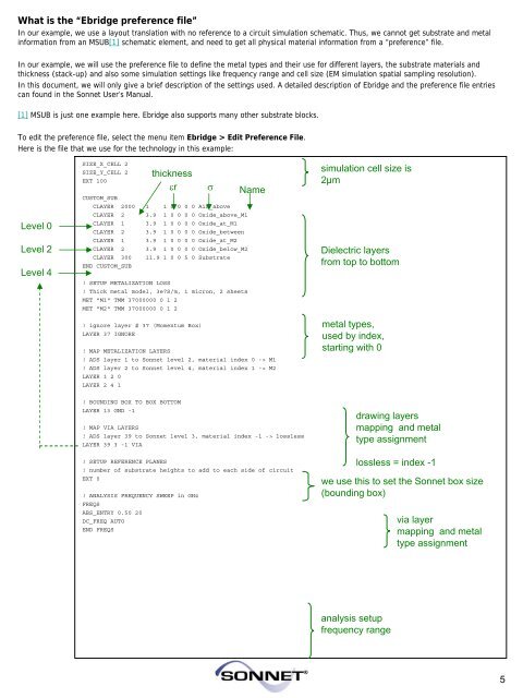
What is the “Ebridge preference file”In our example, we use a layout translation <strong>with</strong> no reference to a circuit simulation schematic. Thus, we cannot get substrate and metalinformation from an MSUB[1] schematic element, and need to get all physical material information from a “preference” file.In our example, we will use the preference file to define the metal types and their use for different layers, the substrate materials andthickness (stack-up) and also some simulation settings like frequency range and cell size (<strong>EM</strong> simulation spatial sampling resolution).In this document, we will only give a brief description of the settings used. A detailed description of Ebridge and the preference file entriescan found in the <strong>Sonnet</strong> User’s Manual.[1] MSUB is just one example here. Ebridge also supports many other substrate blocks.To edit the preference file, select the menu item Ebridge > Edit Preference File.Here is the file that we use for the technology in this example:Level 0Level 2Level 4SIZE_X_CELL 2SIZE_Y_CELL 2EXT 100CUSTOM_SUBCLAYER 2000 1 1 0 0 0 0 Air_aboveCLAYER 2 3.9 1 0 0 0 0 Oxide_above_M1CLAYER 1 3.9 1 0 0 0 0 Oxide_at_M1CLAYER 2 3.9 1 0 0 0 0 Oxide_betweenCLAYER 1 3.9 1 0 0 0 0 Oxide_at_M2CLAYER 2 3.9 1 0 0 0 0 Oxide_below_M2CLAYER 300 11.9 1 0 0 5 0 SubstrateEND CUSTOM_SUB! SETUP METALIZATION LOSS! Thick metal model, 3e7S/m, 1 micron, 2 sheetsMET "M1" TMM 37000000 0 1 2MET "M2" TMM 37000000 0 1 2! ignore layer # 37 (Momentum Box)LAYER 37 IGNOREthicknessεr σ Name! MAP METALIZATION LAYERS! ADS layer 1 to <strong>Sonnet</strong> level 2, material index 0 -> M1! ADS layer 2 to <strong>Sonnet</strong> level 4, material index 1 -> M2LAYER 1 2 0LAYER 2 4 1simulation cell size is2µmDielectric layersfrom top to bottommetal types,used by index,starting <strong>with</strong> 0! BOUNDING BOX TO BOX BOTTOMLAYER 13 GND -1! MAP VIA LAYERS! ADS layer 39 to <strong>Sonnet</strong> level 3, material index -1 -> losslessLAYER 39 3 -1 VIA! SETUP REFERENCE PLANES! number of substrate heights to add to each side of circuitEXT 0! ANALYSIS FREQUENCY SWEEP in GHzFREQSABS_ENTRY 0.50 20DC_FREQ AUTOEND FREQSdrawing layersmapping and metaltype assignmentlossless = index -1we use this to set the <strong>Sonnet</strong> box size(bounding box)via layermapping and metaltype assignmentanalysis setupfrequency range5