VOICE OF THE ENGINEER - ElectronicsAndBooks
VOICE OF THE ENGINEER - ElectronicsAndBooks
VOICE OF THE ENGINEER - ElectronicsAndBooks
- No tags were found...

Create successful ePaper yourself
Turn your PDF publications into a flip-book with our unique Google optimized e-Paper software.
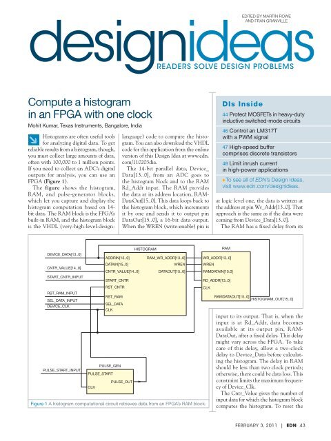
EDITED BY MARTIN ROWEdesignideasAND FRAN GRANVILLEREADERS SOLVE DESIGN PROBLEMSCompute a histogramin an FPGA with one clockMohit Kumar, Texas Instruments, Bangalore, India↘Histograms are often useful toolsfor analyzing digital data. To getreliable results from a histogram, though,you must collect large amounts of data,often with 100,000 to 1 million points.If you need to collect an ADC’s digitaloutputs for analysis, you can use anFPGA (Figure 1).The figure shows the histogram,RAM, and pulse-generator blocks,which let you capture and display thehistogram computation based on 14-bit data. The RAM block is the FPGA’sbuilt-in RAM, and the histogram blockis the VHDL (very-high-level-designlanguage)code to compute the histogram.You can also download the VHDLcode for this application from the onlineversion of this Design Idea at www.edn.com/110203dia.The 14-bit parallel data, Device_Data[13..0], from an ADC goes tothe histogram block and to the RAMRd_Addr input. The RAM providesthe data at its address location, RAM-DataOut[15..0]. This data loops back tothe histogram block, which incrementsit by one and sends it to output pinDataOut[15..0], a 16-bit data output.When the WREN (write-enable) pin isDIs Inside44 Protect MOSFETs in heavy-dutyinductive switched-mode circuits46 Control an LM317Twith a PWM signal47 High-speed buffercomprises discrete transistors48 Limit inrush currentin high-power applications▶To see all of EDN’s Design Ideas,visit www.edn.com/designideas.at logic level one, the data is written atthe address at pin Wr_Addr[13..0]. Thatapproach is the same as if the data werecoming from Device_Data[13..0].The RAM has a fixed delay from itsDEVICE_DATA[13..0]CNTR_VALUE[14..0]START_CNTR_INPUTRST_RAM_INPUTSEL_DATA_INPUTDEVICE_CLKPULSE_START_INPUTADDRIN[13..0]DATAIN[15..0]CNTR_VALUE[14..0]START_CNTRRST_CNTRRST_RAMSEL_DATACLKPULSE_GENPULSE_STARTCLKPULSE_OUTHISTOGRAMRAM_WR_ADDR[13..0]WRENDATAOUT[15..0]Figure 1 A histogram computational circuit retrieves data from an FPGA’s RAM block.RAMWR_ADDR[13..0]WRENRAMDATAIN[15.0]RD_ADDR[13..0]CLKRAMDATAOUT[15..0]HISTOGRAM_OUT[15..0]input to its output. That is, when theinput is at Rd_Addr, data becomesavailable at its output pin, RAM-DataOut, after a fixed delay. This delaymight vary across the FPGA. To takecare of this delay, allow a two-clockdelay to Device_Data before calculatingthe histogram. The delay in RAMshould be less than two clock periods;otherwise, there could be data loss. Thisconstraint limits the maximum frequencyof Device_Clk.The Cntr_Value gives the number ofinput data for which the histogram blockcomputes the histogram. To reset theFEBRUARY 3, 2011 | EDN 43


![[270].pdf 37407KB Sep 02 2010 09:55:57 AM - ElectronicsAndBooks](https://img.yumpu.com/50350834/1/185x260/270pdf-37407kb-sep-02-2010-095557-am-electronicsandbooks.jpg?quality=85)
![draaien, A Viruly 1935 OCR c20130324 [320]. - ElectronicsAndBooks](https://img.yumpu.com/49957773/1/190x252/draaien-a-viruly-1935-ocr-c20130324-320-electronicsandbooks.jpg?quality=85)


![20051110 c20051031 [105].pdf 35001KB Feb 18 2009 08:46:32 PM](https://img.yumpu.com/48687202/1/190x253/20051110-c20051031-105pdf-35001kb-feb-18-2009-084632-pm.jpg?quality=85)