VOICE OF THE ENGINEER - ElectronicsAndBooks
VOICE OF THE ENGINEER - ElectronicsAndBooks
VOICE OF THE ENGINEER - ElectronicsAndBooks
- No tags were found...

You also want an ePaper? Increase the reach of your titles
YUMPU automatically turns print PDFs into web optimized ePapers that Google loves.
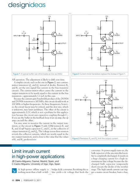
designideas12V12VR 310kR 310kINPUTC 10.1 μFQ 12N3904INPUTC 10.1 μFQ 32N3904D 11N914Q 12N3904R 410kOUTPUTOUTPUTR 110kD 21N914Q 22N3906R 110kQ 22N3906Q 42N3906R 210kR 210k–12VFigure 1 A typical buffer can drive loads as low as 200Ω.–12VFigure 2 Current-mirror transistors replace the diodes in Figure 1.AB operation. The adjustment is likely to drift over time.A simpler circuit, such as the one in Figure 2, uses currentmirrortransistors Q 1and Q 2instead of diodes. Resistors R 2and R 3set the zero-signal bias current in the bias-transistorcircuits. The current-mirror effect causes the current in theoutput transistors to be nearly equal to the current in the biastransistors—approximately 1.2 mA in this case.Because the current-gain-bandwidth product of the 2N3904and 2N3906 transistors is 300 MHz, this circuit should work at100 MHz or higher frequencies. At these frequencies, however,the circuit layout may be critical, and the slew rate, whichis unknown, may limit usefulness. The offset of the circuit isapproximately 0.1V, which is not a problem for this applicationbecause the circuit uses capacitive coupling through C 1.If you use the buffer in the feedback loop of an op amp, the opamp can null the offset.You may want to monitor the current in the output transistors,so the circuit in Figure 3 adds 100Ω resistors R 3andR 4and 10-μF bypass capacitors C 2and C 3in the collectors ofoutput transistors Q 3and Q 4. The voltage across these resistorsreveals the collector currents, which are nearly equal in thetwo output transistors, and is close to the value that the valuesof R 1and R 2predicted.EDNINPUTC 10.1 μFR 510kR 110kR 210kC 210 μFC 310 μF12VQ 12N3904Q 22N3906–12VR 3100Q 32N3904Q 42N3906R 4100Figure 3 Resistors R 3and R 4limit the output current.OUTPUTLimit inrush currentin high-power applicationsJB Castro-Miguens, Cesinel, Madrid, Spain, andC Castro-Miguens, University of Vigo, Vigo, Spain↘A high-power offline supply isnothing more than a half- or fullbridgedc/dc converter. Rectifying the acline yields a dc voltage that feeds theconverter. At power-supply turn-on, thebulk capacitor of the uncontrolled rectifieris completely discharged. It results ina huge charging current for a high instantaneousline voltage because the dischargedbulk capacitor temporarilyshort-circuits the diodes of the rectifierstage. The high inrush current can triggera mains circuit breaker, burn a fuse,48 EDN | FEBRUARY 3, 2011


![[270].pdf 37407KB Sep 02 2010 09:55:57 AM - ElectronicsAndBooks](https://img.yumpu.com/50350834/1/185x260/270pdf-37407kb-sep-02-2010-095557-am-electronicsandbooks.jpg?quality=85)
![draaien, A Viruly 1935 OCR c20130324 [320]. - ElectronicsAndBooks](https://img.yumpu.com/49957773/1/190x252/draaien-a-viruly-1935-ocr-c20130324-320-electronicsandbooks.jpg?quality=85)


![20051110 c20051031 [105].pdf 35001KB Feb 18 2009 08:46:32 PM](https://img.yumpu.com/48687202/1/190x253/20051110-c20051031-105pdf-35001kb-feb-18-2009-084632-pm.jpg?quality=85)