VOICE OF THE ENGINEER - ElectronicsAndBooks
VOICE OF THE ENGINEER - ElectronicsAndBooks
VOICE OF THE ENGINEER - ElectronicsAndBooks
- No tags were found...

You also want an ePaper? Increase the reach of your titles
YUMPU automatically turns print PDFs into web optimized ePapers that Google loves.
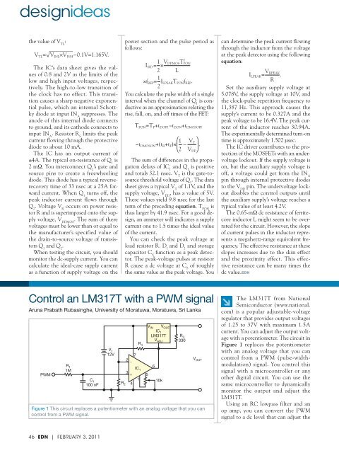
designideasthe value of V TL:V TLV INL V INH 0.1V1.165V.The IC’s data sheet gives the valuesof 0.8 and 2V as the limits of thelow and high input voltages, respectively.The high-to-low transition ofthe clock has no effect. This transitioncauses a sharp negative exponentialpulse, which an internal Schottkydiode at input IN Asuppresses. Theanode of this internal diode connectsto ground, and its cathode connects toinput IN A. Resistor R Slimits the peakcurrent flowing through the protectivediode to about 10 mA.The IC has an output current of±4A. The typical on-resistance of Q 1is2 mΩ. You interconnect Q 2’s gate andsource pins to create a freewheelingdiode. This diode has a typical reverserecoverytime of 33 nsec at a 25A forwardcurrent. When Q 1turns off, thepeak inductor current flows throughQ 2. Voltage V Roccurs on power resistorR and is superimposed onto the supplyvoltage, V DDMOS. The sum of thesevoltages must be lower than or equal tothe manufacturer’s specified value ofthe drain-to-source voltage of transistorsQ 1and Q 2.When testing the circuit, you shouldmonitor the dc-supply current. You cancalculate the ideal-case supply currentas a function of supply voltage on thepower section and the pulse period asfollows:1 V DDMOS T 2 PONI SID = ×2 L1×f REP = I LPEAK T PON f REP .2You calculate the pulse width of a singleinterval when the channel of Q 1is conductiveas an approximation relating therise, fall, on, and off times of the FET:T PONT P +t D<strong>OF</strong>F −t DON +t DMOS<strong>OF</strong>F1−t DMOSON +(t R +t F )× − .2V TV DDThe sum of differences in the propagationdelays of IC 1and Q 1is positiveand totals 32.1 nsec. V Tis the gate-tosourcethreshold voltage of Q 1. The datasheet gives a typical V Tof 1.1V, and thesupply voltage, V DD, has a value of 5V.These values yield 9.8 nsec for the lastterm of the preceding equation. T PONisthus larger by 41.9 nsec. For a good design,an ammeter will indicates a supplycurrent one to 1.5 times the ideal valueof the current.You can check the peak voltage atload resistor R. D 1and D 2and storagecapacitor C Sfunction as a peak detector.The peak-voltage pulses at resistorR cause a dc voltage at C Sof roughlythe same value as the peak voltage. Youcan determine the peak current flowingthrough the inductor from the voltageat the peak detector using the followingequation:VI RPEAKLPEAK .RSet the auxiliary supply voltage at5.078V, the supply voltage at 10V, andthe clock-pulse repetition frequency to11,387 Hz. This approach causes thesupply’s current to be 0.327A and thepeak voltage to be 16.4V. The peak currentof the inductor reaches 30.94A.The experimentally determined turn-ontime is approximately 1.502 μsec.The IC driver contributes to the protectionof the MOSFETs with an undervoltagelockout. If the supply voltage ison, but the auxiliary supply voltage isoff, a voltage could get from the IN Apin through internal protective diodesto the V DDpin. The undervoltage lockoutdisables the control outputs untilthe auxiliary supply’s voltage reaches atypical value of at least 4.2V.The 0.65-mΩ dc resistance of ferritecoreinductor L might seem to be overratedfor the circuit. However, the slopeof current pulses in the inductor representsa megahertz-range equivalent frequency.The effective resistance at theseslopes increases due to the skin effectand the proximity effect. This effectiveresistance can be many times thedc value.EDNControl an LM317T with a PWM signalAruna Prabath Rubasinghe, University of Moratuwa, Moratuwa, Sri LankaPWMR 11MC 1100 nFV 112VV IN V OUTIC 1LM317TR 21410kR 4V ADJR 333072IC 163 5Figure 1 This circuit replaces a potentiometer with an analog voltage that you cancontrol from a PWM signal.V OUT↘The LM317T from NationalSemiconductor (www.national.com) is a popular adjustable-voltageregulator that provides output voltagesof 1.25 to 37V with maximum 1.5Acurrent. You can adjust the output voltagewith a potentiometer. The circuit inFigure 1 replaces the potentiometerwith an analog voltage that you cancontrol from a PWM (pulse-widthmodulation)signal. You control thissignal with a microcontroller or anyother digital circuit. You can use thesame microcontroller to dynamicallymonitor the output and adjust theLM317T.Using an RC lowpass filter and anop amp, you can convert the PWMsignal to a dc level that can adjust the46 EDN | FEBRUARY 3, 2011


![[270].pdf 37407KB Sep 02 2010 09:55:57 AM - ElectronicsAndBooks](https://img.yumpu.com/50350834/1/185x260/270pdf-37407kb-sep-02-2010-095557-am-electronicsandbooks.jpg?quality=85)
![draaien, A Viruly 1935 OCR c20130324 [320]. - ElectronicsAndBooks](https://img.yumpu.com/49957773/1/190x252/draaien-a-viruly-1935-ocr-c20130324-320-electronicsandbooks.jpg?quality=85)


![20051110 c20051031 [105].pdf 35001KB Feb 18 2009 08:46:32 PM](https://img.yumpu.com/48687202/1/190x253/20051110-c20051031-105pdf-35001kb-feb-18-2009-084632-pm.jpg?quality=85)