Ionized physical vapor deposition of integrated circuit interconnects*
Ionized physical vapor deposition of integrated circuit interconnects*
Ionized physical vapor deposition of integrated circuit interconnects*

Create successful ePaper yourself
Turn your PDF publications into a flip-book with our unique Google optimized e-Paper software.
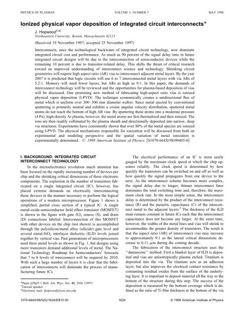
PHYSICS OF PLASMAS VOLUME 5, NUMBER 5 MAY 1998<strong>Ionized</strong> <strong>physical</strong> <strong>vapor</strong> <strong>deposition</strong> <strong>of</strong> <strong>integrated</strong> <strong>circuit</strong> <strong>interconnects*</strong>J. Hopwood †,a)Northeastern University, Boston, Massachusetts 02115Received 19 November 1997; accepted 25 November 1997Interconnects, once the technological backwater <strong>of</strong> <strong>integrated</strong> <strong>circuit</strong> technology, now dominate<strong>integrated</strong> <strong>circuit</strong> cost and performance. As much as 90 percent <strong>of</strong> the signal delay time in future<strong>integrated</strong> <strong>circuit</strong> designs will be due to the interconnection <strong>of</strong> semiconductor devices while theremaining 10 percent is due to transistor-related delay. This shifts the thrust <strong>of</strong> critical researchtoward an improved understanding <strong>of</strong> interconnect science and technology. Shrinking <strong>circuit</strong>geometries will require high aspect ratio AR vias to interconnect adjacent metal layers. By the year2007 it is predicted that logic <strong>circuit</strong>s will use 6 to 7 interconnected metal layers with via ARs <strong>of</strong>5.2:1. Memory will need fewer layers, but ARs as high as 9:1. In this paper, the demands <strong>of</strong>interconnect technology will be reviewed and the opportunities for plasma-based <strong>deposition</strong> <strong>of</strong> viaswill be discussed. One promising new method <strong>of</strong> fabricating high-aspect ratio vias is ionized<strong>physical</strong> <strong>vapor</strong> <strong>deposition</strong> I-PVD. The technique economically creates a unidirectional flux <strong>of</strong>metal which is uniform over 200–300 mm diameter wafers. Since metal ejected by conventionalsputtering is primarily neutral and exhibits a cosine angular velocity distribution, sputtered metalatoms do not reach the bottom <strong>of</strong> high AR vias. By sputtering these atoms into a moderate pressure4Pa, high-density Ar plasma, however, the metal atoms are first thermalized and then ionized. Theions are then readily collimated by the plasma sheath and directionally deposited into narrow, deepvia structures. Experiments have consistently shown that over 80% <strong>of</strong> the metal species are ionizedusing I-PVD. The <strong>physical</strong> mechanisms responsible for ionization will be discussed from both anexperimental and modeling perspective and the spatial variation <strong>of</strong> metal ionization isexperimentally determined. © 1998 American Institute <strong>of</strong> Physics. S1070-664X9890405-0I. BACKGROUND: INTEGRATED CIRCUITINTERCONNECT TECHNOLOGYIn the microelectronics revolution much attention hasbeen focused on the rapidly increasing number <strong>of</strong> devices perchip and the shrinking critical dimensions <strong>of</strong> these electroniccomponents. The explosion in the number <strong>of</strong> transistors fabricatedon a single <strong>integrated</strong> <strong>circuit</strong> IC, however, hasplaced extreme demands on electrically interconnectingthese devices in the manner necessary to perform the logicaloperations <strong>of</strong> a modern microprocessor. Figure 1 shows asimplified, partial cross section <strong>of</strong> a typical IC. A singlemetal-oxide-semiconductor field effect transistor MOSFETis shown in the figure with gate G, source S, and drainD connections labeled. Interconnection <strong>of</strong> this MOSFETwith other devices on the chip not shown is accomplishedthrough the polysilicon/metal alloy silicide gate level andseveral metal-SiO 2 interlayer dielectric ILD levels joinedtogether by vertical vias. Past generations <strong>of</strong> microprocessorsused three metal levels as shown in Fig. 1, but designs usingmore transistors demand additional levels <strong>of</strong> metal. The NationalTechnology Roadmap for Semiconductors 1 forecaststhat 7 to 8 levels <strong>of</strong> interconnect will be required by 2010.With such a large number <strong>of</strong> layers it is clear that the fabrication<strong>of</strong> interconnects will dominate the process <strong>of</strong> manufacturingfuture ICs.*Paper pThpT-1 Bull. Am. Phys. Soc. 42, 2026 1997.† Tutorial speaker.a Electronic mail: jhopwood@lynx.neu.eduThe electrical performance <strong>of</strong> an IC is most easilygauged by the maximum clock speed at which the chip operatesreliably. The clock speed is determined by howquickly the transistors can be switched on and <strong>of</strong>f as well ashow quickly the signal propagates from one device to thenext. As the interconnect scheme becomes more complex,the signal delay due to longer, thinner interconnect linesdominates the total switching time and, therefore, the maximumclock rate. In the most simple sense, the interconnectdelay is determined by the product <strong>of</strong> the interconnect resistanceR and the parasitic capacitance C <strong>of</strong> the interconnectmetal to the adjacent layers. 2 The thickness <strong>of</strong> the ILDmust remain constant in future ICs such that the interconnectcapacitance does not become any larger. At the same time,however, the widths <strong>of</strong> the metal lines and vias will shrink toaccommodate the greater density <strong>of</strong> transistors. The result isthat the aspect ratio AR <strong>of</strong> interconnect vias may increaseto approximately 9:1 as the lateral critical dimensions decreaseto 0.11 m during the coming decade.The fabrication <strong>of</strong> the interconnect structure uses the‘‘damascene’’ method. First a blanket layer <strong>of</strong> ILD is depositedand vias are anisotropically plasma etched. Titanium isdeposited into the via. The titanium acts as an adhesionlayer, but also improves the electrical contact resistance byconsuming residual oxides from the surface <strong>of</strong> the underlyinglayer. It is important to deposit material all the way to thebottom <strong>of</strong> the structure during this step. The success <strong>of</strong> the<strong>deposition</strong> is measured by the bottom coverage which is definedas the ratio <strong>of</strong> Ti film thickness at the bottom <strong>of</strong> the via1070-664X/98/5(5)/1624/8/$15.001624© 1998 American Institute <strong>of</strong> Physics
Phys. Plasmas, Vol. 5, No. 5, May 1998J. Hopwood1625FIG. 1. A partial cross section <strong>of</strong> a simplified <strong>integrated</strong> <strong>circuit</strong>. The expandedview shows a via that is lined with Ti and TiN and subsequentlyfilled with W or Al. Future materials are indicated in parentheses.to the thickness deposited on the top surface <strong>of</strong> the ILD.Next the via receives a barrier layer <strong>of</strong> TiN that protects theILD from corrosive effects <strong>of</strong> WF 6 during chemical <strong>vapor</strong><strong>deposition</strong> <strong>of</strong> the tungsten via plug. Alternately, if aluminumis used as the plug material, the TiN acts as a wetting layerthat allows the sputtered aluminum to be reflowed 3 into thevia at elevated temperatures. In both cases, the TiN acts as adiffusion barrier between the plug and the ILD. The diffusionbarrier must be conformal to the via and it should be asthin as possible so that very little cross sectional area is occupiedby the somewhat resistive barrier material. Finally thelow-resistivity via plug material is deposited. This material isprogressing from W to Al, and eventually Cu. The overburden<strong>of</strong> metal present on the ILD after <strong>deposition</strong> <strong>of</strong> the plugis removed by chemical-mechanical polishing. In the singledamascene process, these step are repeated for the <strong>deposition</strong><strong>of</strong> the metal lines above the vias. A future alternative is thedual damascene process 4 in which the via and metal levelsare etched simultaneously. Then both the via and the metalline are filled with conducting materials and planarized byCMP in the final step. The dual damascene process reducesthe number <strong>of</strong> processing steps needed to fabricate a metallevel, but the requirements on the <strong>deposition</strong> process are considerablymore stringent.Aluminum-0.5% Cu metallization is projected to be replacedby pure copper. 5 Copper has a lower bulk electricalresistivity than AlCu 1.7 vs 3.2 -cm so that the interconnectdelay time RC may be decreased. Equally importantis copper’s ability to conduct higher current densitiesthan AlCu without failure <strong>of</strong> the thin lines due to electromigration<strong>of</strong> the metal atoms. Since copper does not form aself-limiting oxide, copper interconnects will need to becompletely enveloped in a passivating diffusion barrier, mostlikely consisting <strong>of</strong> Ta and TaN layers.Although many technological challenges exist in the areas<strong>of</strong> lithography, low-permittivity dielectric materials andvia etching, this paper will focus on the directional <strong>deposition</strong><strong>of</strong> barrier and plug materials. There are three potentialmethods <strong>of</strong> interconnect <strong>deposition</strong>: Physical <strong>vapor</strong> <strong>deposition</strong>PVD, chemical <strong>vapor</strong> <strong>deposition</strong> CVD, and electroplating.The CVD methods use elevated temperatures orplasma 6 to dissociate precursor species. Filling or lining <strong>of</strong>high aspect ratio features is accomplished by fragmented precursorspecies with low sticking coefficients that are capable<strong>of</strong> reaching and depositing at the bottom <strong>of</strong> deep, narrowopenings. While highly conformal films can be depositedusing CVD, the cost and toxicity <strong>of</strong> the precursor materialsremains an issue. Plating is also an effective way <strong>of</strong> fillinghigh AR features. The plating baths, however, can be difficultto maintain, present a liquid waste hazard, and representa departure from the semiconductor industry’s preference fordry processing. PVD, and in particular sputtering, has longbeen the workhorse <strong>of</strong> the industry. The fundamental problemwith sputtering, however, is the sputtered species areejected from the solid target with a cos n () angulardistribution 7,8 which limits bottom coverage to approximately0.2 in structures with 2:1 ARs. Physical collimation 9<strong>of</strong> the sputtered flux by a honeycomb-shaped filter betweenthe target and wafer improves film conformality by trappingsputtered species with large angle trajectories. Bottomcoverage 10 <strong>of</strong> 2:1 features increases to 0.3–0.4, but the collimatorsignificantly reduces the <strong>deposition</strong> rate and may createparticles that reduce the yield <strong>of</strong> functional ICs.II. IONIZED PHYSICAL VAPOR DEPOSITION „I-PVD…I-PVD is a recent advance in PVD technology thatachieves directional <strong>deposition</strong> <strong>of</strong> metals by ionizing thesputtered or e<strong>vapor</strong>ated metal atoms and collimating theseions with the plasma sheath adjacent to the wafer as shownin Fig. 2. A high electron density (n e 10 11 cm 3 ), inert gasplasma between the target and the wafer is needed to ionizethe metal <strong>vapor</strong>. Strong ionization <strong>of</strong> the metal occurs sincethe electron temperature depends primarily on the ionizationpotential <strong>of</strong> the inert gas 15.7 eV for argon which is muchgreater than that <strong>of</strong> metals 6.0 and 7.7 eV for Al and Cu.The plasma source is commonly an electron cyclotron resonanceplasma 11–13 or inductively coupled plasma. 14–17The average distance that a sputtered neutral will travelbefore being ionized dictates the design <strong>of</strong> an I-PVD system.Simple analysis <strong>of</strong> a sputtered neutral traversing a high densityplasma gives the ionization mean free path 18,19 as iz s /K i n e where s is the velocity <strong>of</strong> the sputtered neutraland K i is the ionization rate constant see below. Atomssputtered from the target exhibit a Thomson distribution 20where the most probable energy is one half the surface bindingenergy (1.5 eV for Al. Therefore, iz 60 cm in anAr plasma where T e 3 eV and n e 510 11 cm 3 . Thisanalysis suggests two methods <strong>of</strong> generating a highly ionized,directional metal flux. First, if the inert gas pressure isquite low, the target-to-wafer distance must be quite long.
Phys. Plasmas, Vol. 5, No. 5, May 1998J. Hopwood1629FIG. 5. Measurement <strong>of</strong> the aluminum ion and neutral density along the axis<strong>of</strong> an I-PVD reactor demonstrates that high ion fractions are achievedthrough he decay <strong>of</strong> the neutral metal density and sustained volume generation<strong>of</strong> metal ions. Solid curves are diffusion models described in the text.The target diameter for this experiment was 75 mm.FIG. 6. The radial variation <strong>of</strong> Al and Al suggests diffusive transport <strong>of</strong>both species. Solid curves are diffusion models described in the text.fusive losses <strong>of</strong> metal to the chamber walls, and 2 approximatelyuniform volume generation <strong>of</strong> metal ions extendingdown to the region near the wafer.Using the same measurement technique, the radial distributions<strong>of</strong> Al and Al adjacent to the surface <strong>of</strong> a 200 mmwafer were determined and are plotted in Fig. 6. Notice thatalthough the bulk ionization fraction Al /AlAl isonly 0.3, the ionized flux fraction is about 0.8 as shown inFig. 3. The aluminum ion density is peaked at the center <strong>of</strong>the wafer and decreases at larger radii. This is a typicaldiffusion-dominated distribution <strong>of</strong> ions as discussed below.To aid in the understanding <strong>of</strong> ionization in an I-PVDreactor, a simple model is proposed. Since the sputteredmetal atoms are thermalized in the first few centimeters nearthe target, transport <strong>of</strong> metal atoms to the wafer is diffusiverather than ballistic. From this observation it is reasonable toattempt a solution to the diffusion equation for metal atoms 2 n M (r,z)0 in a cylinder R, L with the boundary conditionthat M 0 at the chamber walls. The sputteringsource <strong>of</strong> M is modeled with a boundary adjacent to thetarget that is the sum <strong>of</strong> k disks, each <strong>of</strong> constant Al densityand concentric about the central axis at z 0,kn M r,z0N 0 A i 1urb i ,i118where u is the unit step function and the constants b i and A iare chosen to match the erosion pr<strong>of</strong>ile <strong>of</strong> the target. Thediffusion solution isn M r,z2N 0i1kb iA J1 x 0 j b i /RiR j0 x 0 j J 2 1 x 0 j 0 J x 0 jrR expk zzexpk z z2L1exp2k z L , 19where J n is the n th -order Bessel function <strong>of</strong> the first kind,k z x 0 j /R, and J 0 (x 0 j )0. The modeled aluminum neutraldensity Eq. 19 is plotted along with the experimentalmeasurements in Figs. 5 and 6. Only the magnitude <strong>of</strong> thedensity N 0 ) was scaled to fit the data. The agreement <strong>of</strong> thediffusion model for the Al distribution is within the accuracy<strong>of</strong> the experiment. The right hand side <strong>of</strong> Fig. 7 shows acontour plot <strong>of</strong> the neutral density Al superimposed on asketch <strong>of</strong> an I-PVD reactor with R22 cm and L15 cm.It has previously been shown that sputtered atoms mustbe thermalized if ionization is to occur within the confines <strong>of</strong>the I-PVD reactor. Since the metal ions are thermalized, it isreasonable to assume that the ion density distribution will bediffusive as well. The Klyarfeld parabolic approximation 25has been shown to predict the distribution <strong>of</strong> ions in inductivelycoupled plasmas. 45 By combining the Klyarfeld solutionfor a long tube n T (r) with the solution for an infiniteslab geometry n S (z), an estimate <strong>of</strong> the ion density within acylinder is n M (r,z)n T (r)n S (z) wheren T rn io11h R n S zn io11h l zL/2Rr 2, 202L/2 ,21h l 0.86,223L/2 iand h R is given in Eq. 6. Figures 5 and 6 show that thisapproximate solution for aluminum ion density agrees wellwith respect to z but predicts a metal ion density that is moreuniform along the radial direction than experimentally observed.The left hand side <strong>of</strong> Fig. 7 shows a contour plot <strong>of</strong>the Klyarfeld parabolic approximation within a typical Al I-PVD reactor at 10 mTorr. Finally, although the uniformity<strong>of</strong> the <strong>deposition</strong> rate over 200 mm wafers was typically7%–13%, the fraction <strong>of</strong> ionized flux is much more uniformsince the diffusion dominated metal and metal ion densitiesdecrease radially at similar rates. There are several unifor-
1630 Phys. Plasmas, Vol. 5, No. 5, May 1998 J. HopwoodFIG. 7. Contour plots <strong>of</strong> aluminum neutral and ion density in a 44 cm diameter I-PVD reactor.mity issues yet to be resolved, but bottom coverage which isproportional to ionization fraction should be quite consistentacross large wafers.V. CONCLUSION<strong>Ionized</strong> <strong>physical</strong> <strong>vapor</strong> <strong>deposition</strong> is a viable techniquefor the fabrication <strong>of</strong> high aspect ratio interconnects for futuregenerations <strong>of</strong> <strong>integrated</strong> <strong>circuit</strong>s. The advantages <strong>of</strong> I-PVD over the alternative methods are numerous: The metalsource is a nontoxic low-cost solid, the process does notproduce chemical wastes, sputtering is a very clean process,and sputtering has a well-established technology base in theIC fabrication industry. The most promising applications forI-PVD are for the <strong>deposition</strong> <strong>of</strong> liners and barriers—the refilling<strong>of</strong> high aspect ratio vias with metal is an area whereadditional research is required.Ionization <strong>of</strong> sputtered species is most effective whenthe ionization potential <strong>of</strong> the inert gas is much greater thanthe metal. Metals with low ion mobility will also exhibithigher fractional ionization. Reactor geometry is shown toinfluence ionization. These factors include designing the reactorwith sufficient target-to-wafer spacing so that thermalization<strong>of</strong> sputtered atoms occurs within the high densityplasma. Uniformity <strong>of</strong> the <strong>deposition</strong> rate and bottom coveragedepend on the distribution <strong>of</strong> ions and the fraction <strong>of</strong>ionized flux. The ion flux fraction is inherently uniform sincediffusive transport applies to both metal neutrals and ions.Further research and development are needed to control theuniformity <strong>of</strong> ions at the wafer. Finally, while the body <strong>of</strong>knowledge for directional metal <strong>deposition</strong> using inert gasI-PVD is maturing, the physics, gas-phase chemistry, andprocess technology <strong>of</strong> nitride <strong>deposition</strong> TiN, TaN, andWN is not yet well-understood for I-PVD processes.ACKNOWLEDGMENTSThe author wishes to acknowledge the assistance <strong>of</strong> M.Dickson and G. Zhong.This work is currently supported by the National ScienceFoundation and U.S. Department <strong>of</strong> Energy under Grant No.DMR-9712988.1 National Technology Roadmap for Semiconductors Semiconductor IndustryAssociation, San Jose, CA, 1994.2 S. P. Murarka, Metallization: Theory and Practice for VLSI and ULSIButterworth-Heinemann, Boston, 1993.3 H. Liao and T. S. Cale, J. Vac. Sci. Technol. B 14, 2615 1996, andreferences therein.4 S. M. Rossnagel, J. Vac. Sci. Technol. B 13, 125 1995.5 P. F. Cheung, S. M. Rossnagel, and D. N. Ruzic, J. Vac. Sci. Technol. B13, 203 1995.6 J. Faltermeier, A. Knorr, R. Talevi, H. Gundlach, K. A. Kumar, G. G.Peterson, A. E. Kaloyeros, J. J. Sullivan, and J. Loan, J. Vac. Sci. Technol.B 15, 1758 1997.7 H. H. Andersen, B. Stenum, T. Sorensen, and H. Whitlow, Nucl. Instrum.Methods Phys. Res. B 6, 459 1985.8 Y. Yamamura and M. Ishida, J. Vac. Sci. Technol. A 13, 101 1995.9 S. M. Rossnagel, D. Mikalsen, H. Kinsohita, and J. J. Cuomo, J. Vac. Sci.Technol. A 9, 261 1991.10 R. Powell private communication, 1996.11 T. Ono, C. Takahashi, and S. Matsuo, Jpn. J. Appl. Phys. 23, L534 1984.12 W. M. Holber, J. S. Logan, J. J. Grabarz, J. T. C. Yeh, J. B. O. Caughman,A. Sugerman, and F. E. Turene, J. Vac. Sci. Technol. A 11, 2903 1993.13 C. Doughty, S. M. Gorbatkin, T. Y. Tsui, G. M. Pharr, and D. L. Medlin,J. Vac. Sci. Technol. A 15, 2623 1997.14 M. Yamashita, J. Vac. Sci. Technol. A 7, 151 1989.15 M. Yamashita, J. Vac. Sci. Technol. A 7, 2752 1989.16 S. M. Rossnagel and J. Hopwood, Appl. Phys. Lett. 63, 3285 1993.17 S. M. Rossnagel and J. Hopwood, J. Vac. Sci. Technol. B 12, 449 1994.18 S. M. Rossnagel, Thin Solid Films 263, 11995.19 M. Dickson and J. Hopwood, J. Vac. Sci. Technol. A 15, 2307 1997.20 M. W. Thompson, Philos. Mag. 18, 377 1968.21 S. Hamaguchi and S. M. Rossnagel, J. Vac. Sci. Technol. B 14, 26031996.22 C. A. Nichols, S. M. Rossnagel, J. Vac. Sci. Technol. B 14, 3270 1996.23 J. Hopwood and F. Qian, J. Appl. Phys. 78, 758 1995.24 M. A. Lieberman and A. J. Lichtenberg, Principles <strong>of</strong> Plasma Discharges
Phys. Plasmas, Vol. 5, No. 5, May 1998J. Hopwood1631and Materials Processing Wiley, New York, 1994, p. 140.25 V. A. Godyak, Soviet Radio Frequency Discharge Research Delphic,Falls Church, VA, 1986, p. 79ff.26 B. E. Cherrington, Gaseous Electronics and Gas Lasers Pergamon Press,Oxford, 1979, p. 119.27 L. M. Chanin and M. A. Biondi, Phys. Rev. 107, 1219 1957.28 A. H. Futch and F. A. Grant, Phys. Rev. 104, 356 1956.29 T. Holstein, Phys. Rev. 83, 1159 1951.30 L. A. Riseberg, W. F. Parks, and L. D. Schearer, Phys. Rev. A 8, 19621973.31 M. A. Biondi and L. M. Chanin, Phys. Rev. 94, 910 1954.32 K. B. McAfee, D. Siple, and D. Edelson, Phys. Rev. 160, 130 1967.33 F. J. de Heer, R. H. Jansen, and W. van der Kaay, J. Phys. B: Atom.Molec. Phys. 12, 979 1979.34 L. Vriens, Phys. Lett. 8, 260 1964.35 D. Rapp and P. Englander-Golden, J. Chem. Phys. 43, 1464 1965.36 L. L. Shimon, E. I. Nepiipov, and I. P. Zapesochnyi, Sov. Phys. Tech.Phys. 20, 434 1975.37 M. A. Lennon, K. L. Bell, H. B. Gilbody, J. G. Hughes, A. E. Kingston,M. J. Murray, and F. J. Smith, J. Phys. Chem. Ref. Data 17, 1285 1988.38 W. Lotz, Z. Phys. 232, 101 1970, and references therein.39 M. Dickson, F. Qian, and J. Hopwood, J. Vac. Sci. Technol. A 15, 3401997.40 S. M. Rossnagel, J. Vac. Sci. Technol. A 6, 191988.41 J. W. Coburn and E. Kay, Appl. Phys. Lett. 18, 435 1971.42 B. E. Cherrington, Gaseous Electronic and Gas Lasers Pergamon Press,Oxford, 1979, p. 169.43 A. Gras-Marti and J. A. Valles-Abarca, J. Appl. Phys. 54, 1071 1983.44 L. T. Ball, I. S. Falconer, D. R. McKenzie, and J. M. Smelt, J. Appl. Phys.59, 720 1986.45 N. Forgotson, V. Khemka, and J. Hopwood, J. Vac. Sci. Technol. B 14,732 1996.