CHAPTER 4 BIPOLAR JUNCTION TRANSISTORS (BJTs)
CHAPTER 4 BIPOLAR JUNCTION TRANSISTORS (BJTs)
CHAPTER 4 BIPOLAR JUNCTION TRANSISTORS (BJTs)

Create successful ePaper yourself
Turn your PDF publications into a flip-book with our unique Google optimized e-Paper software.
<strong>CHAPTER</strong> 4 <strong>BIPOLAR</strong> <strong>JUNCTION</strong> <strong>TRANSISTORS</strong> (<strong>BJTs</strong>)Chapter Outline4.1 Device Structure and Physical Operation4.2 Current-Voltage Characteristics4.3 BJT Circuits at DC4.4 Applying the BJT in Amplifier Design4.5 Small-Signal Operation and Models4.6 Basic BJT Amplifier Configurations4.7 Biasing in BJT Amplifier Circuits48 4.8 Discrete-Circuit DiscreteCircuit BJT AmplifiersNTUEE Electronics – L. H. Lu 4-1
4.1 Device Structure and Physical OperationPhysical structure of bipolar junction transistor (BJT)Both electrons and holes participate in the conduction process for bipolar devices.BJT consists of two pn junctions constructed in a special way and connected in series, back to back.The transistor is a three-terminal device with emitter, base and collector terminals.From the physical structure, <strong>BJTs</strong> can be divided into two groups: npn and pnp transistors.Modes of operationThe two junctions of BJT can be either forward or reverse-biased.The BJT can operate in different modes depending on the junction bias.The BJT operates in active mode for amplifier circuits.Switching applications utilize both the cutoff and saturation modes.Mode EBJ CBJCutoff Reverse ReverseActive Forward ReverseSaturation Forward ForwardNTUEE Electronics – L. H. Lu 4-2
Operation of the npn transistor in the active modeElectrons in emitter regions are injected into base due to the forward bias at EBJ.Most of the injected electrons reach the edge of CBJ before being recombined if the base is narrow.Electrons at the edge of CBJ will be swept into collector due to the reverse bias at CBJ.Emitter injection efficiency () = i En / ( i En + i Ep )Base transport factor ( T ) = i Cn / i EnCommon-base current gain ( ) = i Cn / i E = T < 1Terminal currents of BJT in active mode:i E (emitter current) = i En (electron injection from E to B) + i Ep (hole injection from B to E)i C (collector current) = i Cn (electron drift) + i CBO (CBJ reverse saturation current with emitter open)i B (base current) = i B1 (hole injection from B to E) + i B2 (recombination in base region)NTUEE Electronics – L. H. Lu 4-3
Terminal currents:Collector current: iC iCn AEqDnBdnBx) / dx AEqDnBBase current:• Hole injection into emitter due to forward bias:• Eelectron-hole recombination in base:• Total base current:Emitter current:iE iCiB iB i 1 iCE nB i vBE/ VT( (0) / e DiNi IC S eB2v BE / V TnBiWA qD nN WB1 AEqDpEdpEx)/12 Qn/ n AEqW2pE BB1 iB2 IS( )DnBNELpE2 DnBn1WevBE/ VB2( dx nB(0) W / nTiCAIESNeEvqDBELB/ VpEpEAEqWn2NnTn2i2ieev BE / V Tv BE / V TNTUEE Electronics – L. H. Lu 4-4
Large-signal model and current gain for BJT in active regionCommon-emitter current gainCommon-base current gain(1)i Bi Ei C(+1)i Ci E1i BC pE B1Common-emitter current gain: ( ) /(1 )i D N L 2 D Common-base current gain: iB /( 1)The structure of actual transistorsIn modern process technologies, the BJT utilizes a vertical structure.Typically, is smaller and close to unity while is large.DnBNEWpE1WnB12nNTUEE Electronics – L. H. Lu 4-5
Operation of the npn transistor in the saturation modeSaturation mode: both EBJ and CBJ are forward biasedCarrier injection from both emitter and collector into baseBase minority carrier concentraiton change accordingly leading to reduced slope as v BC increasesCollector current drops from the value in active mode for negative v CBFor a given v BE , i C drops sharply to zero at v CB around 0.5 V and v CE around 0.2 V.BJT in saturation: V CEsat = 0.2 ViCCurrent gain reduces from to forced : forcediBsaturationn p0 exp(v BE /V T ) n p0 exp(v BC /V T )v BC increasesn p0NTUEE Electronics – L. H. Lu 4-6
Ebers-Moll modelIn EM model, the EBJ and CBJ are represented by two back to back diodes i DE and i DC .The current transported from one junction to the other is presented by F (forward) and R (reverse).EM model can be used to describe the BJT in any of its possible modes of operation.EM model is used for more detailed dc analysis which can not be performed by the simplified models.v /The diode currents: ( BE VTv /iDEISEe 1) ( BC VTiDCISCe 1)FISE RISC ISThe terminal currents: i i i i ii i i iApplication of the EM modelThe forward active mode:iiiCBEv /V1BE / VT ISe IS1R I S vBE/ V 1 1T e ISF FRI S vBE/ V 1Te I S1F F The saturation mode:iiiCEB I I ISeSESEveBEv/ VBET/ VT ISC ISeevvBCBC/ VT/ VTEDEvBE/ VT( 1) e I (1 FSCR) evBCR DC/ VTCDCFDEi EBECi DE R i DCi Bi DC F i DEi CNTUEE Electronics – L. H. Lu 4-7
The cutoff mode• I CBO (CBJ reverse current with emitter open-circuited)I CBO = (1 R F )I SCBoth EBJ and CBJ are reverse-biased.In real case, reverse current depends on v CB .• I CEO (CBJ reverse current with base open-circuited)I CEO = I CBO /(1 F ) F is always smaller than unity such that I CEO > I CBO .CBJ current flows from (C to B) so CBJ is reverse-biased.EBJ current flows from (E to B) so EBJ is slightly forward-biased.Ei E = 0Bi B +(3) R I SC R F I SC (4)(2) R I SCI SC (1)i Ci C = I CBO = (1 R F )I SC (5)CEBi B = 0(3) i DE F i DE (4)I SC (1) +i B = ( R )I SC + ( F )i DE = 0 i DE = I SC ( R ) / ( F ) (5)i C = I SC + F i DE = I SC (1 R F )/ (1 F ) I CEO = I CBO / ( F ) (6)i CCNTUEE Electronics – L. H. Lu 4-8
The pnp transistorTransistor structure:• emitter and collector are p-type• base is n-typeOperation of pnp is similar to that of npnOperation of pnp in the active modeCollector current:Base current:Emitter current: iiCiB i C/ E i ICSe iv EB / V TBLarge-signal model and current gain for BJTin active regionCommon-emitter current gainCommon-base current gain(1)i Bi Ei C(+1)i Ci E1i B1NTUEE Electronics – L. H. Lu 4-9
Current-voltage characteristics of BJTThe i C -v CB characteristicsThe i C -v CE characteristicsThe Early effectAs CBJ reverse bias increases, the effective base width W eff reduces due to the increasing CBJ depletion.For a constant junction voltage v BE :• The slope of n B (x) increases i C increasesn B (0)V Z• Charge storage Q n reduces i B decreasesV Y• Current gain and increasesV XEarly voltage (V A ) is used for the linear approximation of Early Effect.vBE/ VTLinear dependence of i C on v CE :Exhibit finite output resistance:iC ISe i(1 v/ VCE A1Cro vBE constant vCE)VIACn B00 W X W Y W ZNTUEE Electronics – L. H. Lu 4-11
Common-base output characteristicsEarly effectbreakdowni C versus v CB plot with various i E as parameter is known as common-base output characteristicsThe slope indicates that i C depends to a small extent on v CB Early effecti C increases rapidly at high v CB breakdownBCJ is slightly forward-biased for 0.4V < v CB < 0No significant change is observed in i CThe BJT still exhibits I-V characteristics as in the active modeBCJ turns on strongly and the i C starts to decrease for v BC < 0.4V• I-V characteristics in the saturation mode and v CEsat is considered a constant ( 0.2 V)Current gain (): large-signal i C /i E and small-signal (incremental) i C /i ENTUEE Electronics – L. H. Lu 4-12
Common-emitter output characteristics (I)i C versus v CE plot with various v BE as parameter.Common-emitter current gain is defined as = i C / i BThe BCJ turns on with a positive v BC at low v CEBJT operates in saturation modeThe i C curve has a finite slope due to Early effectThe characteristics lines meet at v CE = V AV A is called the Early Voltage (~ 50 to 100 V)Common-emitter output characteristics (II)Plot of i C versus v CE with various i B as parameterBJT in active region acts as a current sourcewith high (but finite) output resistanceThe cutoff mode in common-emitter configurationis defined as i B = 0Current gain: large-signal dc i C /i B and ac i C /i BEarly effectbreakdownNTUEE Electronics – L. H. Lu 4-13
Saturation of common-emitter configurationIn saturation region, it behaves as a closed switch with a small resistance R CEsatThe saturation IV curve can be approximated by a straight line intersecting the v CE axis at V CEoffThe saturation voltage V CEsat V CEoff + I Csat R CEsatV CEsat is normally treated as a constant of 0.2 V for simplicity regardless the value of i CIncremental in saturation is lower than that in active region: forced I Csat / I B < Overdrive factor / forcedNTUEE Electronics – L. H. Lu 4-14
Transistor breakdownTransistor breakdown mechanism:• Avalanche breakdown: avalanche multiplication mechanism takes place at CBJ or EBJ• Base punch-through effect: the base width reduces to zero at high CBJ reverse biasIn CB configuration, BV CBO is defined at i E = 0.The breakdown voltage is smaller than BV CBO for i E > 0.In CE configuration, BV CEO is defined at i B =0.The breakdown voltage is smaller than BV CEO for i B > 0.Typically, BV CEO is about half of BV CBO .Breakdown of the BCJ is not destructive as long as the power dissipation is kept within safe limits.Breakdown of the EBJ is destructive because it will cause permanent degradation of NTUEE Electronics – L. H. Lu 4-15
4.3 BJT Circuits at DCBJT operation modesThe BJT operation mode depends on the voltages at EBJ and BCJThe I-V characteristics are strongly nonlinearSimplified models and classifications are needed to speed up the hand-calculation analysisMode EBJ CBJnpn transistorpnp transistorSaturation Forward ForwardInverse Reverse ForwardCutoff Modev BE 0, v BC 0v BECutoff Modev EB 0, v CB 0v EBActive Forward ReverseCutoff Reverse ReverseInverse Modev BE 0, v BC 0v BCActive Modev BE 0, v BC 0Saturation Modev BE 0, v BC 0Inverse Modev EB 0, v CB 0v CBActive Modev EB 0, v CB 0Saturation Modev EB 0, v CB 0Simplified models and classifications for the operation of the npn BJTCut-off mode:• i E = i C = i B = 0• v BE < 0.5 V and v BC < 0.4 VActive mode:• v BE = 0.7 V and i B : i C : i E = 1: : (1+)• v CE > 0.3 VSaturation mode:• v BE = 0.7 V and v CE = 0.2 V• i C /i B = forced < NTUEE Electronics – L. H. Lu 4-16
Biasing the circuit to obtain linear amplificationThe slope in the VTC indicates voltage gainBJT in active mode can be used as voltage amplificationPoint Q is known as bias point or dc operating pointI C = I S exp(V BE /V T )The signal to be amplified is superimposed on V BEv BE (t) = V BE + v be (t)The time-varying part in v CE (t) is the amplified signalThe circuit can be used as a linear amplifier if:• A proper bias point is chosen for gain• The input signal is small in amplitudeThe small-signal voltage gainThe amplifier gain is the slope at Q:AvdvdvCEBEvBEVBEI VVoltage gain depends on I C and R CMaximum voltage gain of the amplifierICAv VTRCVCCTCTVVCERCVVCCTA|v max|NTUEE Electronics – L. H. Lu 4-21
Determining the VTC by graphical analysisProvides more insight into the circuit operationLoad line: the straight line represents in effect the loadi C = (V CC V CE )/R CThe operating point is the intersection pointLocating the bias point QThe bias point (intersection) is determined by properly choosing the load lineThe output voltage is bounded by V CC (upper bound) and V CEsat (lower bound)The load line determines the voltage gainThe bias point determines the headroom or maximum upper/lower voltage swing of the amplifierNTUEE Electronics – L. H. Lu 4-22
4.5 Small-Signal Operation and ModelsThe collector current and the transconductanceThe total quantities (ac + dc) of the collector current:viCBE V ISeBEvBE v/ VbeIT VBE/ VTvbe/ VT ( ) SeSmall-signal approximation: v be
The emitter current and the input resistance at the emitterThe total quantities (ac + dc) of the emitter current:iE IE ieI Small-signal approximation:eERelation between r and r e :CImCiicgmICie vbe v VTvbeVT 1re i I g gr ergmgmmcbeIV r ( 1 )r eOutput resistance accounting for Early effectETvbeUse the collector current equation with linear v CE dependence: v V vBE / T CEiCISe1 VA1 iCVro vBE constant vCE IACThe output resistance r o is included to represent Early Effect of the BJTThe resulting r o is typically a large resistance and can be neglected to simplify the analysisNTUEE Electronics – L. H. Lu 4-24
BJT small-signal modelsTwo models are exchangeable and does not affect the analysis resultThe hybrid- model• Typically used as the emitter is groundedNeglect r oThe T model• Typically used as the emitter is not groundedNeglect r oNTUEE Electronics – L. H. Lu 4-25
Three basic configurations4.6 Basic BJT Amplifier ConfigurationCommon-Emitter (CE) Common-Base (CB) Common-Collector (CC)Characterizing amplifiersThe BJT circuits can be characterized by a voltage amplifier model (unilateral model)The electrical properties of the amplifier is represented by R in , R o and A voThe analysis is based on the small-signal or linear equivalent circuit where dc components are not includedVoltage gain:AOverall voltage gain:vvvoiRLRL RvoGvvosigAvoRinRin RsigAvRinRin RsigRLR RLsoAvoNTUEE Electronics – L. H. Lu 4-26
The common-emitter (CE) amplifierCharacteristic parameters of the CE amplifier• Input resistance: R in r • Output resistance: Ro RC|| ro RC• Open-circuit voltage gain: Avogm(RC|| ro• Voltage gain: A gR || R || r ) g( R• Overall voltage gain:vm ) g(C L o m C|| RL)rrGv gm( RC|| RL|| ro) gm( RC|| RL)r Rr RCE amplifier can provide high voltage gain.Input p and output are out of phase due to negative gain.Lower I C increases R in at the cost of voltage gain.Output resistance is moderate to high.Small R C reduces R o at the cost of voltage gain.sigmRCsigNTUEE Electronics – L. H. Lu 4-27
The common-emitter (CE) with an emitter resistanceCharacteristic parameters (by neglecting r o )• Input resistance:Rin ( 1 )( re Re) r (1 ) Re• Output resistance:Ro R C• Open-circuit voltage gain:AvogmRC 1R / r• Voltage gain:AvegmRC 1g RegmRC 1g R• Overall voltage gain:Gv rrmeRLR RLgRCmegm(RC|| RL) 1g REmitter degeneration resistance R e is adopted.Input resistance is increased by adding (1+)R e .Gain is reduced by the factor (1+g m R e ).The overall gain is less dependent on .It is considered a negative feedback of the amplifier.Rm m C LRsig1gmReRL RCrer Rsiggm(RC|| RL)1g RmeNTUEE Electronics – L. H. Lu 4-28
The common-base (CB) amplifierCharacteristic parameters of the CE amplifier (by neglecting r o )• Input resistance: Rin r e• Output resistance: Ro R C• Open-circuit voltage gain: Avo gmRC• Voltage gain: A g R || R )• Overall voltage gain:vm( C L( RC|| RL)CE amplifier can provide high voltage gain.Input p and output are in-phase due to positive gain.Gvrer RInput resistance is very low.A single CB stage is not suitable for voltage amplification.Output resistance is moderate to high.Small R C reduces R o at the cost of voltage gain.The amplifier is no longer unilateral if r o is included.esiggmNTUEE Electronics – L. H. Lu 4-29
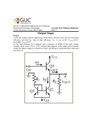
The common-collector (CC) amplifierCharacteristic parameters of the CC amplifier (by neglecting r o )• Input resistance: Rin ( 1 )( re RL)• Output resistance: Ro re Rsig/ • Open-circuit voltage gain: A R /( R r ) 1• Overall voltage gain:GvRinvoRin RsigLLRLR rLee( 1)RL( 1)(R r ) RLesig 1CC amplifier is also called emitter follower.Input resistance is very high.Output resistance is very low.The voltage gain is less than but can be close to 1.CC amplifier can be used as voltage buffer.It is noted that, in the analysis, the amplifier is not unilateral.NTUEE Electronics – L. H. Lu 4-30
DC bias for BJT amplifier4.7 Biasing in BJT Amplifier CircuitsThe amplifiers are operating at a proper dc bias point.Linear signal amplification is provided based on small-signal circuit operation.The DC bias circuit is to ensure the BJT in active mode with a proper collector current I C .The classical discrete-circuit bias arrangementA single power supply and resistors are neededThevenin equivalent circuit:• V BB = V CC R 2 /(R 1 +R 2 )• R B = R 1 ||R 2BJT operating point:ICRBV BBVBE/ R (1 1/ )ER C is chosen to ensure the BJT in active (V CE > V CEsat ).A two-power-supply version of the classical bias arrangementTwo power supplies are neededSimilar dc analysisBJT operating point:ICRBVEEVBE/ R (1 1/ )ENTUEE Electronics – L. H. Lu 4-31
Biasing using a collector-to-base feedback resistorA single power supply is needed.R B ensures the BJT in active (V CE > V BE 0.7 V)CC BEBJT operating point: ICRB/ RC(1 1/ )The value of the feedback resistor R B affects the small-signal gain.Biasing using a constant-current sourceThe BJT can be biased with a constant current source I.The resistor R C is chosen to operate the BJT in active mode.VThe current source is typically implemented by a BJT current mirror.Current mirror circuit:• Both BJT transistors Q 1 and Q 2 are in active mode.• Assume current gain is very high:I IREFVCCVREEVBEV• When applying to the amplifier circuit, the voltageV has to be high enough to ensure Q 2 in active.NTUEE Electronics – L. H. Lu 4-32
4.8 Discrete-Circuit BJT AmplifiersCircuit analysis:DC analysis:• Remove all ac sources (short for voltage source and open for current source)• All capacitors are considered open-circuit• DC analysis of BJT circuits for all nodal voltages and branch currents• Find the dc current I C and make sure the BJT is in active modeAC analysis:• Remove all dc sources (short for voltage source and open for current source)• All large capacitors are considered short-circuit• Replace the BJT with its small-signal signal model for ac analysis• The circuit parameters in the small-signal model are obtained based on the value of I CComplete amplifier circuitDC equivalent circuitAC equivalent circuitNTUEE Electronics – L. H. Lu 4-33
The common-emitter (CE) amplifierThe common-emitter amplifier with an emitter resistanceNTUEE Electronics – L. H. Lu 4-34
The common-base (CB) amplifierThe common-collector (CC) amplifierNTUEE Electronics – L. H. Lu 4-35
The amplifier frequency responseThe gain falls off at low frequency band due to the effects of the coupling and by-pass capacitorsThe gain falls off at high frequency band due to the internal capacitive effects in the <strong>BJTs</strong>Midband:• All coupling and by-pass capacitors (large capacitance) are considered short-circuit• All internal capacitive effects (small capacitance) are considered open-circuit• Midband gain is nearly constant and is evaluated by small-signal analysis• The bandwidth is defined as BW = f H – f L• A figure-of-merit for the amplifier is its gain-bandwidth product defined as GB = |A M |BWNTUEE Electronics – L. H. Lu 4-36