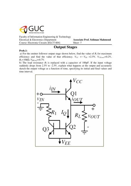
Sheet 7 - GUC - Faculty of Information Engineering & Technology
Sheet 7 - GUC - Faculty of Information Engineering & Technology
Sheet 7 - GUC - Faculty of Information Engineering & Technology
- No tags were found...

Create successful ePaper yourself
Turn your PDF publications into a flip-book with our unique Google optimized e-Paper software.
Prob.2:(a) For the shown Emitter follower shown, assume V CC =12V, V BE,ON =0.7V,V CE,sat =0.2V, I Q2 =I=5mA, R L =650 and =100. Determine the value <strong>of</strong> R .(b) Determine the critical value <strong>of</strong> the load resistance to avoid clipping (distortion).(c) Calculate the peak to peak output voltage swing if R L =650 .(d) Calculate the peak to peak output voltage swing and the conversion efficiency ifRL=2.5K (e) Use PSPICE to plot the transfer function <strong>of</strong> the emitter follower for the values inpart(a)Note: The PSPICE model <strong>of</strong> the diode and BJT:.MODEL D1N914 D(IS=100E-15 RS=16 BV=100 IBV=100E-15).MODEL Q NPN(BF=100 VA=100)
Prob.4:Six versions <strong>of</strong> a source follower are shown below. Assume that µ n C Ox = 2 µ p C Ox , P =2 N , all W/L ratios <strong>of</strong> all devices are equal, and that all bias currents in each device areequal. Neglect bulk effects in this problem and assume no external load resistor.Identify which circuit or circuits have the following characteristics:(a.) highest small-signal voltage gain,(b.) lowest small-signal voltage gain,(c.) the highest output resistance,(d.) the lowest output resistance,(e.) the highest v out(max) and(f.) the lowest v out(max) .
Prob.6:(a) Design a V BE multiplier for class AB amplifier shown in order to provide thebiasing current I bias =5.67mA.Assume V CC =12V, V BE =0.7 V, and R L =50. Assumea minimum current <strong>of</strong> the VBE multiplier circuit is 1mA and the DC biasingcurrent <strong>of</strong> Q n and Q p I C =2mA .(b) Use PSPICE to plot the transfer characteristic and the instantaneous i Cn , i Cp and i Lfor v I= 5sin(2000πt) V.Notes:(a)The PSPICE model <strong>of</strong> the diode and BJT:.MODEL Q NPN(IS= 1E-14 BF=100 VJE=0.7).MODEL Qn NPN(IS= 1E-14 BF=50 VJE=0.7).MODEL Qp PNP(IS= 1E-14 BF=50 VJE=0.7).MODEL Qp1 PNN(IS= 1E-14 BF=100 VJE=0.7); TRANSISTORS USED TOREALIZE I bias.(a) In this problem, you need to do DC and transient analysisDC analysis to plot the transfer function: .DC vin -12 12 0.001Transient analysis: .Tran 5U 2MS ; 2 PERIODES FROM SINWAVE.