Lab 5: Analog to Digital Conversion 5.1 Introduction 5.2 DAC ...
Lab 5: Analog to Digital Conversion 5.1 Introduction 5.2 DAC ...
Lab 5: Analog to Digital Conversion 5.1 Introduction 5.2 DAC ...

You also want an ePaper? Increase the reach of your titles
YUMPU automatically turns print PDFs into web optimized ePapers that Google loves.
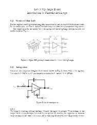
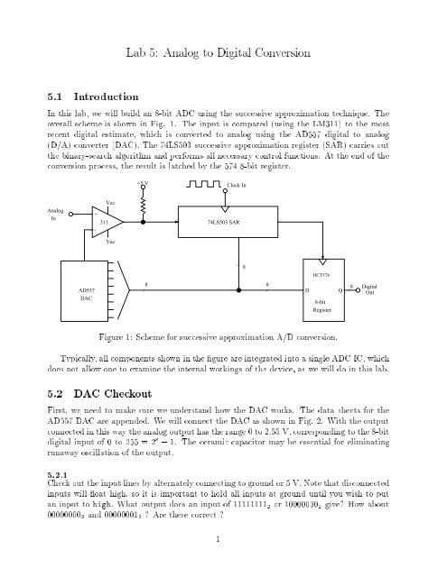
<strong>Lab</strong> 5: <strong>Analog</strong> <strong>to</strong> <strong>Digital</strong> <strong>Conversion</strong><strong>5.1</strong> <strong>Introduction</strong>In this lab, we will build an 8-bit ADC using the successive approximation technique. Theoverall scheme is shown in Fig. 1. The input is compared (using the LM311) <strong>to</strong> the mostrecent digital estimate, which isconverted <strong>to</strong> analog using the AD557 digital <strong>to</strong> analog(D/A) converter (<strong>DAC</strong>). The 74LS503 successive approximation register (SAR) carries outthe binary-search algorithm and performs all necessary control functions. At the end of theconversion process, the result is latched by the 574 8-bit register.+5 V Clock In<strong>Analog</strong>InVcc+311-Vee74LS503 SARHCT574AD557<strong>DAC</strong>8/8/_ 8/ 8D8-bitRegisterQ<strong>Digital</strong>OutFigure 1: Scheme for successive approximation A/D conversion.Typically, all components shown in the gure are integrated in<strong>to</strong> a single ADC IC, whichdoes not allow one <strong>to</strong> examine the internal workings of the device, as we will do in this lab.<strong>5.2</strong> <strong>DAC</strong> CheckoutFirst, we need <strong>to</strong> make surewe understand how the<strong>DAC</strong> works. The data sheets for theAD557 <strong>DAC</strong> are appended. We will connect the <strong>DAC</strong> asshown in Fig. 2. With the outputconnected in this way the analog output has the range 0 <strong>to</strong> 2:55 V, corresponding <strong>to</strong> the 8-bitdigital input of 0 <strong>to</strong> 255 = 2 8 , 1. The ceramic capaci<strong>to</strong>r may be essential for eliminatingrunaway oscillation of the output.<strong>5.2</strong>.1Check out the input lines by alternately connecting <strong>to</strong> ground or 5 V. Note that disconnectedinputs will oat high, so it is important <strong>to</strong> hold all inputs at ground until you wish <strong>to</strong> putan input <strong>to</strong> high. What output does an input of 11111111 2 or 10000000 2 give? How about00000000 2 and 00000001 2 ? Are these correct ?1
LSB12161514131211109<strong>Analog</strong> Out0-2.55 V<strong>Digital</strong>In3456AD557Vcc (+5V)MSB78CSCE~0.1 UF, ceramicFigure 2: Connection scheme for AD557 <strong>DAC</strong>. The CS and CE control functions won't beneeded for this lab and should be connected <strong>to</strong> ground, as shown.<strong>5.2</strong>.2Look at V out on the oscilloscope. How does the dierence between 00000000 2 and 00000001 2compare <strong>to</strong> the level of noise? Qualitatively, what kind of frequency spectrum does the noisehave? (That is, which frequencies, if any, seem <strong>to</strong> be most noticeable?)5.3 A/D in Slow MotionNow we can connect the successive approximation register (SAR) and voltage compara<strong>to</strong>r<strong>to</strong> make our rst ADC circuit. The detailed connection scheme is shown in Fig. 3. We willbegin by evaluating this ADC in slow motion, clocking it by hand. The pin connections forthe LM311 compara<strong>to</strong>r are shown in Fig. 4.To enable hand clocking of the SAR, use the pro<strong>to</strong>type board debounced switches connectedas shown in Fig. 5. Finally, provide an adjustable DC analog input by connectingthe analog input (at the 10k resis<strong>to</strong>r) <strong>to</strong> the variable resis<strong>to</strong>r of the pro<strong>to</strong>type board, asshown in Fig. 6.5.3.1Connect the 8 pro<strong>to</strong>type board LEDs <strong>to</strong> the SAR outputs Q0 { Q7 so that the present digitalestimate can be directly viewed. Finally, we need <strong>to</strong> see when the SAR has completed itsconversion cycle: The CC pin goes LOW when the cycle is complete. Connect a separate redLED with a current-limiting resis<strong>to</strong>r ( 470 ), as shown in Fig. 3. The LED should be oduring conversion and turn on when conversion is complete. Finally, notethatpin1oftheSAR is \chip enable" (E); this must be grounded.5.3.2The SAR is a \synchronous" device, so it will start conversion only when the S signal isaccompanied by aclock pulse. Give your device some analog input (measure with a DVMor scope). Now start the conversion and watch the analog estimate (output of <strong>DAC</strong>) with aDVM and the digital estimate (LEDs) while issuing additional clock pulses by hand. Thebinary search pattern should be evident.2
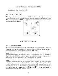
+5 VIN10k4.7MVcc2 +3113 -Vee7+5 V1k7DClock In974LS503 SARQ0 --- Q73 14Start10CC__E1Vcc (+5)1682470LED161__ 8AD557<strong>DAC</strong>8/8/LEDs8Figure 3: Connections for slowA/Dcheckout. Consult the data sheet for the pin assignmentsfor the SAR outputs Q 0 {Q 7 .Ground18VccIn 1In 223+_76OutputVee4 5LM311Figure 4: Connections for the LM311 voltage compara<strong>to</strong>r. We should not need <strong>to</strong> use thebalance adjustment (pins 5 and 6) for this lab. For this lab, use VCC +6 and VEE ,6V.3
+5V+5VNCNO~1kclockNCNO~1kSFigure 5: Debounced switch connections for clock (left) and start = S (right).+51k<strong>Analog</strong> In10k23+-311Figure 6: Providing an adjustable analog input.4
How many clock pulses occur from start <strong>to</strong> end of conversion?Carefully measure 6 input analog values including zero and full scale, and ll out a tablewith the following 4 headings:V in V <strong>DAC</strong> Expected <strong>Digital</strong> Out Measured <strong>Digital</strong> Out (LEDs)Is the response linear? Make a plot of digital output vs V in . Estimate the maximumnon-linearity over the full input range. Is it consistent withLSB=2 ? Is there an oset?5.4 Normal Speed CheckoutSetupcontinuous cycling operation by replacing the S but<strong>to</strong>n with a connection from CC.That is, directly connect pin 2 <strong>to</strong> pin 10. Replace the clock but<strong>to</strong>n input with one from theTTL output of the pro<strong>to</strong>type board function genera<strong>to</strong>r. Run the clock frequency somewherein the range 10 kHz <strong>to</strong> 100 kHz.5.4.1Connect a scope probe <strong>to</strong> the <strong>DAC</strong> output. Trigger the scope on CC. Now watch theconversion process on the scope. Vary the analog input and watch your ADC converge <strong>to</strong>the input value. Compare what you see <strong>to</strong> Fig. 9.52A of Horowitz and Hill.5.4.2There is a 2 MHz function genera<strong>to</strong>r in the lab. Replace your pro<strong>to</strong>type board clock with thisone. Watch the conversion process while increasing the clock frequency. You will probablynotice a lot of parasitic capacitive coupling at the highest frequencies. But beyond this noise,does the nal ADC value remain steady with increasing frequency? Is there a breakdownfrequency, where the conversion no longer works properly?5.4.3Now we will make a pretty display. As before, connect the clock <strong>to</strong> the pro<strong>to</strong>type boardclock. Use a frequency of few10 4 Hz. Using an external function genera<strong>to</strong>r, give your ADCan input consisting of a triangle wave of frequency 100 Hz and amplitude which spansthe range of your ADC. Set up the scope as before. You should now see the entire binarysearch pattern on the scope, as your ADC attempts <strong>to</strong> converge <strong>to</strong> all possible input values.By carefully tuning the two frequencies it is possible <strong>to</strong> get a (nearly) stationary pattern.Compare with Horowitz and Hill Fig. 9.52B.Use the oscilloscope camera <strong>to</strong> snap a picture of your trace <strong>to</strong> include in your report. (Note:for a normally bright scope trace, a shutter speed of 0.25 <strong>to</strong> 0.5 sec works OK. After pullingthe pho<strong>to</strong> from the camera, let it process for 90 sec before removing the chemical backing.)5.5 Completing the ADCAny real ADC will have a digital output which islatched and s<strong>to</strong>red at the end of theconversion cycle. This will be done using the 8-bit D-type positive edge-triggered register5
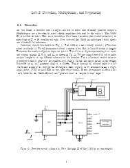
(HCT574) shown in Fig. 7. Connect up the HCT574 as shown, connecting the LEDs <strong>to</strong> itsoutputs.SARLogic XVcc (+5)<strong>DAC</strong>8/__ 8/823456789D0D1D2D3D4D5D6D7OE111 20HCT57410Q0Q1Q2Q3Q4Q5Q6Q71918171615141312ToLEDsFigure 7: Connections for latching the digital output.5.<strong>5.1</strong>We need <strong>to</strong> provide a clock signal <strong>to</strong> latch the output at the end of the conversion cycle.A clear candidate for this signal would be the rising edge of the CC signal of the SAR as itreturns from LOW <strong>to</strong> HIGH. Try using this. Vary the analog input and watch the LEDs. Youshould nd that one of the LEDs never lights up. Which one? The reason for this can beseen from the timing diagram of Fig. 8. The rising edge of CC occurs <strong>to</strong>o late, after the nextcycle has begun. Similarly, the falling edge of CC is <strong>to</strong>o early. In this case, the LSB wouldnever be set.By examining Fig. 8, can you nd a single digital gate which provides the pulse we want,labelled \X" in Fig. 7. Connect this up and draw your \logic X" box. You will probablyneed <strong>to</strong> consult one of the TTL books in the lab <strong>to</strong> get the right IC and connection scheme.With this connection, verify that all digital bits can now belatched.ClockCCXFigure 8: Timing for output register latching.6