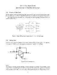
Lab 5: Analog to Digital Conversion 5.1 Introduction 5.2 DAC ...
Lab 5: Analog to Digital Conversion 5.1 Introduction 5.2 DAC ...
Lab 5: Analog to Digital Conversion 5.1 Introduction 5.2 DAC ...

Create successful ePaper yourself
Turn your PDF publications into a flip-book with our unique Google optimized e-Paper software.
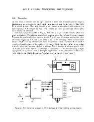
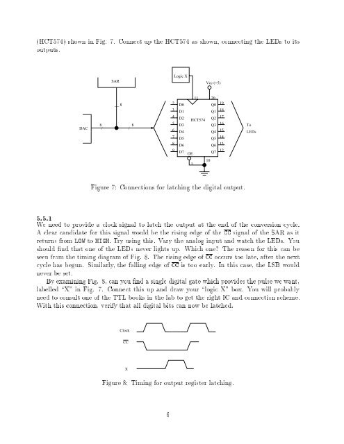
(HCT574) shown in Fig. 7. Connect up the HCT574 as shown, connecting the LEDs <strong>to</strong> itsoutputs.SARLogic XVcc (+5)<strong>DAC</strong>8/__ 8/823456789D0D1D2D3D4D5D6D7OE111 20HCT57410Q0Q1Q2Q3Q4Q5Q6Q71918171615141312ToLEDsFigure 7: Connections for latching the digital output.5.<strong>5.1</strong>We need <strong>to</strong> provide a clock signal <strong>to</strong> latch the output at the end of the conversion cycle.A clear candidate for this signal would be the rising edge of the CC signal of the SAR as itreturns from LOW <strong>to</strong> HIGH. Try using this. Vary the analog input and watch the LEDs. Youshould nd that one of the LEDs never lights up. Which one? The reason for this can beseen from the timing diagram of Fig. 8. The rising edge of CC occurs <strong>to</strong>o late, after the nextcycle has begun. Similarly, the falling edge of CC is <strong>to</strong>o early. In this case, the LSB wouldnever be set.By examining Fig. 8, can you nd a single digital gate which provides the pulse we want,labelled \X" in Fig. 7. Connect this up and draw your \logic X" box. You will probablyneed <strong>to</strong> consult one of the TTL books in the lab <strong>to</strong> get the right IC and connection scheme.With this connection, verify that all digital bits can now belatched.ClockCCXFigure 8: Timing for output register latching.6