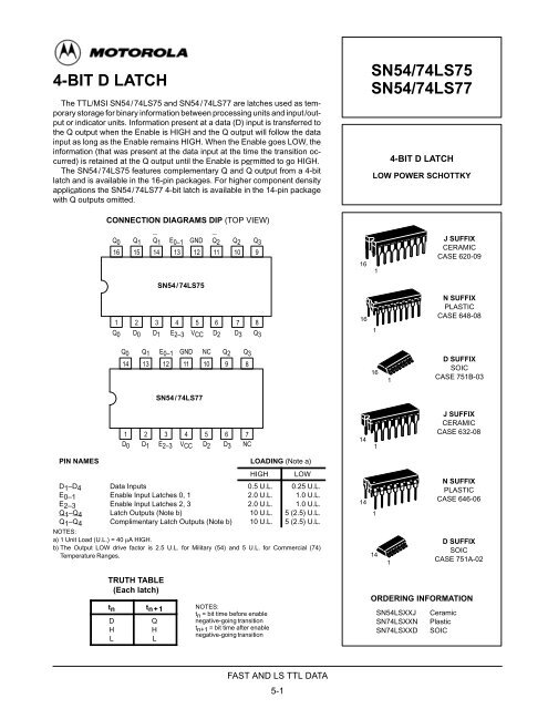
4-BIT D LATCH SN54/74LS75 SN54/74LS77
4-BIT D LATCH SN54/74LS75 SN54/74LS77
4-BIT D LATCH SN54/74LS75 SN54/74LS77
- No tags were found...

You also want an ePaper? Increase the reach of your titles
YUMPU automatically turns print PDFs into web optimized ePapers that Google loves.
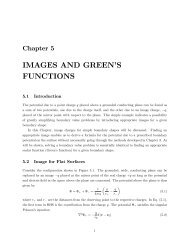
4-<strong>BIT</strong> D <strong>LATCH</strong>The TTL/MSI <strong>SN54</strong>/<strong>74LS75</strong> and <strong>SN54</strong>/<strong>74LS77</strong> are latches used as temporarystorage for binary information between processing units and input/outputor indicator units. Information present at a data (D) input is transferred tothe Q output when the Enable is HIGH and the Q output will follow the datainput as long as the Enable remains HIGH. When the Enable goes LOW, theinformation (that was present at the data input at the time the transition occurred)is retained at the Q output until the Enable is permitted to go HIGH.The <strong>SN54</strong>/<strong>74LS75</strong> features complementary Q and Q output from a 4-bitlatch and is available in the 16-pin packages. For higher component densityapplications the <strong>SN54</strong>/<strong>74LS77</strong> 4-bit latch is available in the 14-pin packagewith Q outputs omitted.<strong>SN54</strong>/<strong>74LS75</strong><strong>SN54</strong>/<strong>74LS77</strong>4-<strong>BIT</strong> D <strong>LATCH</strong>LOW POWER SCHOTTKYCONNECTION DIAGRAMS DIP (TOP VIEW)Q0 Q1 Q1 E0–1 GND Q2 Q2 Q316 15 14 13 12 11 10 9161J SUFFIXCERAMICCASE 620-09<strong>SN54</strong>/<strong>74LS75</strong>1 2 3 4 5 6 7 8Q0 D0 D1 E2–3 VCC D2 D3 Q3161N SUFFIXPLASTICCASE 648-08Q0 Q1 E0–1 GND NC Q2 Q314 13 12 11 10 9 8161D SUFFIXSOICCASE 751B-03<strong>SN54</strong>/<strong>74LS77</strong>1 2 3 4 5 6 7D0 D1 E2–3 VCC D2 D3 NC141J SUFFIXCERAMICCASE 632-08PIN NAMES LOADING (Note a)HIGH LOWD1–D4E0–1E2–3Q1–Q4Q1–Q4Data InputsEnable Input Latches 0, 1Enable Input Latches 2, 3Latch Outputs (Note b)Complimentary Latch Outputs (Note b)0.5 U.L.2.0 U.L.2.0 U.L.10 U.L.10 U.L.0.25 U.L.1.0 U.L.1.0 U.L.5 (2.5) U.L.5 (2.5) U.L.NOTES:a) 1 Unit Load (U.L.) = 40 µA HIGH.b) The Output LOW drive factor is 2.5 U.L. for Military (54) and 5 U.L. for Commercial (74)Temperature Ranges.141141N SUFFIXPLASTICCASE 646-06D SUFFIXSOICCASE 751A-02TRUTH TABLE(Each latch)tnDHLtn+1QHLNOTES:t n = bit time before enablenegative-going transitiont n+1 = bit time after enablenegative-going transitionORDERING INFORMATION<strong>SN54</strong>LSXXJ CeramicSN74LSXXN PlasticSN74LSXXD SOICFAST AND LS TTL DATA5-1
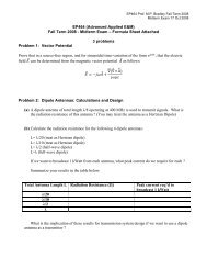
<strong>SN54</strong>/<strong>74LS75</strong>LOGIC SYMBOLS<strong>SN54</strong>/<strong>74LS75</strong><strong>SN54</strong>/<strong>74LS77</strong>2 3 6 71 2 5 6134D0E0–1D1 D2 D3E2–3Q0 Q0 Q1 Q1 Q2 Q2 Q3 Q3VCC = PIN 5GND = PIN 12123D0E0–1D1 D2 D3E2–3Q0 Q1 Q2 Q3VCC = PIN 4GND = PIN 11NC = PIN 7, 1016 1 15 14 10 11 9 814 13 9 8DC CHARACTERISTICS OVER OPERATING TEMPERATURE RANGE (unless otherwise specified)LimitsSymbol Parameter Min Typ Max Unit Test ConditionsiVIH Input HIGH Voltage 2.0 VVILInput LOW Voltage54 0.774 0.8VGuaranteed Input HIGH Voltage forAll InputsGuaranteed Input LOW Voltage forAll InputsVIK Input Clamp Diode Voltage –0.65 –1.5 V VCC = MIN, IIN = – 18 mAVOHVOLOutput HIGH VoltageOutput LOW Voltage54 2.5 3.5 V VCC = MIN, IOH = MAX, VIN = VIH74 2.7 3.5 Vor VIL per Truth Table54, 74 0.25 0.4 V IOL = 4.0 mA VCC = VCC MIN,VIN =VIL or VIH74 0.35 0.5 V IOL = 8.0 mA per Truth TableIIHInput HIGH CurrentD InputE InputD InputE Input20800.10.4µA VCC = MAX, VIN = 2.7 VmAVCC = MAX, VIN = 7.0 VIILInput LOW CurrentD InputE Input–0.4–1.6mAVCC = MAX, VIN = 0.4 VIOS Short Circuit Current (Note 1) –20 –100 mA VCC = MAXICC Power Supply Current 12 mA VCC = MAXNote 1: Not more than one output should be shorted at a time, nor for more than 1 second.AC CHARACTERISTICS (TA = 25°C, VCC = 5.0 V)LimitsSymbol Parameter Min Typ Max Unit Test ConditionsitPLHtPHLPropagation Delay, Data to Q159.02717nstPLHtPHLtPLHtPHLPropagation Delay, Data to QPropagation Delay, Enable to Q127.0151420152725nsnsVCC = 5.0 VCL = 15 pFtPLHtPHLPropagation Delay, Enable to Q167.03015nsFAST AND LS TTL DATA5-2
<strong>SN54</strong>/<strong>74LS77</strong>DC CHARACTERISTICS OVER OPERATING TEMPERATURE RANGE (unless otherwise specified)LimitsSymbol Parameter Min Typ Max Unit Test ConditionsiVIH Input HIGH Voltage 2.0 VVILInput LOW Voltage54 0.774 0.8VGuaranteed Input HIGH Voltage forAll InputsGuaranteed Input LOW Voltage forAll InputsVIK Input Clamp Diode Voltage –0.65 –1.5 V VCC = MIN, IIN = – 18 mAVOHVOLOutput HIGH VoltageOutput LOW Voltage54 2.5 3.5 V VCC = MIN, IOH = MAX, VIN = VIH74 2.7 3.5 Vor VIL per Truth Table54, 74 0.25 0.4 V IOL = 4.0 mA VCC = VCC MIN,VIN =VIL or VIH74 0.35 0.5 V IOL = 8.0 mA per Truth TableIIHInput HIGH CurrentD InputE InputD InputE Input20800.10.4µA VCC = MAX, VIN = 2.7 VmAVCC = MAX, VIN = 7.0 VIILInput LOW CurrentD InputE Input–0.4–1.6mAVCC = MAX, VIN = 0.4 VIOS Short Circuit Current (Note 1) –20 –100 mA VCC = MAXICC Power Supply Current 13 mA VCC = MAXNote 1: Not more than one output should be shorted at a time, nor for more than 1 second.AC CHARACTERISTICS (TA = 25°C, VCC = 5.0 V)LimitsSymbol Parameter Min Typ Max Unit Test ConditionsitPLHtPHLtPLHtPHLPropagation Delay, Data to QPropagation Delay, Enable to Q119.0101019171818nsnsVCC = 5.0 VCL = 15 pFFAST AND LS TTL DATA5-3
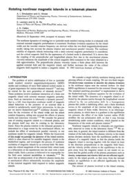
<strong>SN54</strong>/<strong>74LS75</strong> <strong>SN54</strong>/<strong>74LS77</strong>DATAENABLETO OTHER <strong>LATCH</strong>LOGIC DIAGRAMQ (<strong>SN54</strong>/<strong>74LS75</strong> ONLY)QGUARANTEED OPERATING RANGESSymbol Parameter Min Typ Max UnitVCC Supply Voltage 54744.54.755.05.05.55.25VTA Operating Ambient Temperature Range 5474–550252512570°CIOH Output Current — High 54, 74 –0.4 mAIOL Output Current — Low 54744.08.0mAAC SETUP REQUIREMENTS (TA = 25°C, VCC = 5.0 V)Symbol Parameter MinLimitsTyp Max Unit Test ConditionsitW Enable Pulse Width High 20 nsts Setup Time 20 ns VCC = 5.0 Vth Hold Time 0 nsAC WAVEFORMSDE1.3 V 1.3 Vtsth1.3 V 1.3 V 1.3 VtPLHQtPLH1.3 V tPHL1.3 VtPHLQtPHL1.3 VtPLH1.3 VtPHLtPLHDEFINITION OF TERMSSETUP TIME (ts) — is defined as the minimum time required for the correct logic level to be present at the logic input prior to theclock transition from HIGH-to-LOW in order to be recognized and transferred to the outputs.HOLD TIME (th) — is defined as the minimum time following the clock transition from HIGH-to-LOW that the logic level must bemaintained at the input in order to ensure continued recognition. A negative HOLD TIME indicates that the correct logic level maybe released prior to the clock transition from HIGH-to-LOW and still be recognized.FAST AND LS TTL DATA5-4