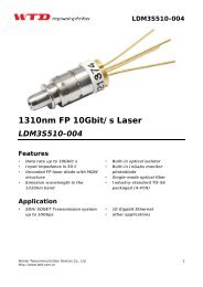
RTXM166-401
RTXM166-401
RTXM166-401
- No tags were found...

Create successful ePaper yourself
Turn your PDF publications into a flip-book with our unique Google optimized e-Paper software.
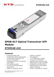
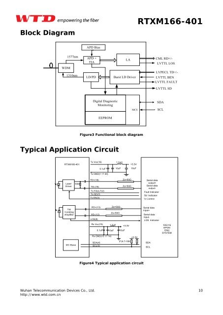
Block Diagram<strong>RTXM166</strong>-<strong>401</strong>APD BiasWDM1577nm1310nmAPD +TIALD/PDLABurst LD DriverCML RD+/-LVTTL LOSLVPECL TD+/-LVTTL BENLVTTL FAULTLVTTL SDDigital DiagnosticMonitoringMCUSDASCLEEPROMFigure3 Functional block diagramTypical Application Circuit<strong>RTXM166</strong>-<strong>401</strong>Tx Vcc(16)1.2uH+3.3V0.1uF 10uF 10uFTx GND(1 17 20)LaserDriver100ΩTD+(18)TD-(19)Tx FAULT(2)Tx SD(7)Tx EN(3)Zo=50ΩZo=50ΩSerial dataoutput+Serial dataoutput-Fault IndicatorSd IndicatorTx ControlTIA+LimitingAmplifierRD+(13)RD-(12)LOS(8)Zo=50ΩZo=50ΩSerial datainput+Serial datainput-LOS IndicatorRx Vcc(15)1.2uH0.1uF 10uF 10uFRx GND(10 11 14)+3.3V+3.3V10G/1GEPONONUSYSTEMI2C SlaveSDA(4)SCL(5)2*(4.7-10K)SDASCLFigure4 Typical application circuitWuhan Telecommunication Devices Co., Ltd.http://www.wtd.com.cn10