Bluetooth/ISM 2.4-GHz Front-End IC T7024 - DigiKey
Bluetooth/ISM 2.4-GHz Front-End IC T7024 - DigiKey
Bluetooth/ISM 2.4-GHz Front-End IC T7024 - DigiKey
- No tags were found...

You also want an ePaper? Increase the reach of your titles
YUMPU automatically turns print PDFs into web optimized ePapers that Google loves.
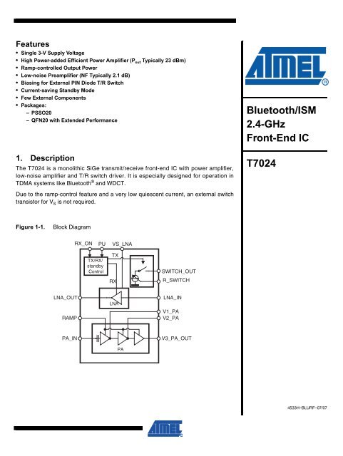
Features• Single 3-V Supply Voltage• High Power-added Efficient Power Amplifier (P out Typically 23 dBm)• Ramp-controlled Output Power• Low-noise Preamplifier (NF Typically 2.1 dB)• Biasing for External PIN Diode T/R Switch• Current-saving Standby Mode• Few External Components• Packages:– PSSO20– QFN20 with Extended Performance<strong>Bluetooth</strong>/<strong>ISM</strong><strong>2.4</strong>-<strong>GHz</strong><strong>Front</strong>-<strong>End</strong> <strong>IC</strong>1. DescriptionThe <strong>T7024</strong> is a monolithic SiGe transmit/receive front-end <strong>IC</strong> with power amplifier,low-noise amplifier and T/R switch driver. It is especially designed for operation inTDMA systems like <strong>Bluetooth</strong> ® and WDCT.Due to the ramp-control feature and a very low quiescent current, an external switchtransistor for V S is not required.<strong>T7024</strong>Figure 1-1.Block DiagramRX_ONPUVS_LNATX/RX/standbyControlTXRXSWITCH_OUTR_SWITCHLNA_OUTRAMPLNALNA_INV1_PAV2_PAPA_INPAV3_PA_OUT4533H–BLURF–07/07
V2_PAV2_PAGNDV1_PAPA_INGNDVS_LNAGNDLNA_INGND2. Pin ConfigurationFigure 2-1. Pinning PSSO20 Figure 2-2. Pinning QFN20R_SWITCH120PUSWITCH_OUT219RX_ONGND318LNA_OUTLNA_INVS_LNAGNDV3_PA_OUT4567<strong>T7024</strong>17161514GNDPA_INV1_PAGNDV3_PA_OUTV3_PA_OUTV3_PA_OUTGNDRAMP1112131410 9 8 7 6<strong>T7024</strong>1516 17 18 19 2054321SWITCH_OUTR_SWITCHPURX_ONLNA_OUTV3_PA_OUT813V2_PAV3_PA_OUT912V2_PAGND1011RAMPTable 2-1. Pin DescriptionPins PSSO20 Pins QFN20 Symbol Function1 4 R_SWITCH Resistor to GND sets the PIN diode current2 5 SWITCH_OUT Switched current output for PIN diode3 6 GND Ground4 7 LNA_IN Low-noise amplifier input5 9 VS_LNA Supply voltage input for low-noise amplifier6 8 GND Ground7 11 V3_PA_OUT Inductor to power supply and matching network for power amplifier output8 12 V3_PA_OUT Inductor to power supply and matching network for power amplifier output9 13 V3_PA_OUT Inductor to power supply and matching network for power amplifier output10 10 GND Ground11 15 RAMP Power ramping control input12 16 V2_PA Inductor to power supply for power amplifier13 17 V2_PA Inductor to power supply for power amplifier14 14 GND Ground15 19 V1_PA Supply voltage for power amplifier16 20 PA_IN Power amplifier input17 18 GND Ground18 1 LNA_OUT Low-noise amplifier output19 2 RX_ON RX active high20 3 PU Power-up active highSlug Slug GND Ground2<strong>T7024</strong>4533H–BLURF–07/07
<strong>T7024</strong>3. Absolute Maximum RatingsStresses beyond those listed under “Absolute Maximum Ratings” may cause permanent damage to the device. This is a stress ratingonly and functional operation of the device at these or any other conditions beyond those indicated in the operational sections of thisspecification is not implied. Exposure to absolute maximum rating conditions for extended periods may affect device reliability.Parameters Symbol Value UnitSupply voltagePins VS_LNA, V1_PA, V2_PA, V3_PA_OUTV S 6 VJunction temperature T j 150 °CStorage temperature T stg –40 to +125 °CRF input power LNA P inLNA 5 dBmRF input power PA P inPA 10 dBmElectrostatic sensitive device.Observe precautions for handling.4. Thermal ResistanceParameters Symbol Value UnitJunction ambient PSSOP20, slug soldered on PCB R thJA 19 K/WJunction ambient QFN20, slug soldered on PCB R thJA 27 K/W5. HandlingDo not operate this part near strong electrostatic fields. This <strong>IC</strong> meets class 1 ESD test requirement(HBM in accordance to EIA/JESD22-A114-A (October 97) and class A ESD testrequirement (MM) in accordance to EIA/JESD22-A115A.6. Operating RangeAll voltages are referred to ground (pins GND and slug). Power supply points are VS_LNA, V1_PA, V2_PA, V3_PA_OUT.The table represents the sum of all supply currents depending on the TX/RX mode.Parameters Symbol Min. Typ. Max. UnitSupply voltagePins V1_PA, V2_PA and V3_PA_OUTV S 2.7 3.0 4.6 VSupply voltage, pin VS_LNA V S 2.7 3.0 5.5 VSupply current TX, PSSO20QFN20Supply current RXI SISI S1901658mAmAmAStandby current, PU = 0 I S_standby 10 µAAmbient temperature T amb –25 +25 +85 °C4533H–BLURF–07/073
7. Electrical CharacteristicsTest conditions (unless otherwise specified): V S = 3.0V, T amb = 25°CParameters Test Conditions Symbol Min. Typ. Max. UnitPower Amplifier (1)Supply voltage Pins V1_PA, V2_PA, V3_PA_OUT V S 2.7 3.0 4.6 VTX, PSSO20TX, QFN20I S_TXI S_TX190165Supply currentRX (PA off), V RAMP ≤ 0.1V I S_RX 10 µAStandby current Standby I S_standby 10 µAFrequency range TX f <strong>2.4</strong> 2.5 <strong>GHz</strong>Gain-control range TX ∆Gp 60 42 dBPower gain maximum TX, pin PA_IN to V3_PA_OUT Gp 28 30 33 dBPower gain minimum TX, pin PA_IN to V3_PA_OUT Gp –40 –17 dBRamping voltage maximumTX, power gain (maximum)Pin RAMPmAmAV RAMP max 1.7 1.75 1.83 VTX, power gain (minimum)Ramping voltage minimumVPin RAMPRAMP min 0.1 VRamping current maximum TX, V RAMP = 1.75V, pin RAMP I RAMP max 0.5 mAPower-added efficiencyTX, PSSO20TX, QFN20Saturated output powerTX, input power = 0 dBm referred topins V3_PA_OUTP sat 22 23 24 dBmInput matching (2)TX, pin PA_INLoadVSWR< 1.5:1Output matching (2)TX, pins V3_PA_OUTLoadVSWR< 1.5:1Harmonics at P sat = 23 dBmTX, pins V3_PA_OUT 2 fo –30 dBcTX, pins V3_PA_OUT 3 fo –30 dBcT/R Switch Driver (Current Programming by External Resistor from R_SWITCH to GND)Standby, pin SWITCH_OUT I S_O_standby 1 µARX I S_O_RX 1 µASwitch-out current outputTX at 100Ω I S_O_100 1.7 mATX at 1.2 kΩ I S_O_1k2 7 mATX at 33 kΩ I S_O_33k 17 mATX at ∞ I S_O_R 19 mALow-noise Amplifier (3)Supply voltage All, pin VS_LNA V S 2.7 3.0 5.5 VSupply current RX I S 8 9 mANotes: 1. Power amplifier shall be unconditionally stable, maximum duty cycle 100%, true CW operation, maximum load mismatchand duration: load VSWR = 10:1 (all phases) 10s, Z G = 50Ω.2. With external matching network, load impedance 50Ω.3. Low-noise amplifier shall be unconditionally stable.4. With external matching components.5. LNA gain can be adjusted with RX_ON voltage according to Figure 9-16 on page 11. Please note, that for RX_ON below1.4V the T/R switch driver switches to TX mode.PAEPAE30353540%%4<strong>T7024</strong>4533H–BLURF–07/07
<strong>T7024</strong>7. Electrical Characteristics (Continued)Test conditions (unless otherwise specified): V S = 3.0V, T amb = 25°CParameters Test Conditions Symbol Min. Typ. Max. UnitSupply current(LNA and control logic)TX (control logic active)Pin VS_LNAI S 0.5 mAStandby current Standby, pin VS_LNA I S_standby 1 10 µAFrequency range RX f <strong>2.4</strong> 2.5 <strong>GHz</strong>Power gain (5) RX, pin LNA_IN to LNA_OUT Gp 15 16 19 dBNoise figureRX, PSSO20RX, QFN20Gain compression RX, referred to pin LNA_OUT O1dB –9 –7 –6 dBm3 rd -order input interception point RX IIP3 –16 –14 –13 dBmInput matching (4) RX, pin LNA_IN VSWRin 2:1Output matching (4) RX, pin LNA_OUT VSWRout 2:1Logic Input Levels (RX_ON, PU) (5)High input level = ‘1’ pins RX_ON and PU V iH <strong>2.4</strong> V S, LNA VLow input level = ‘0’ V iL 0 0.5 VHigh input current = ‘1’ V iH = <strong>2.4</strong>V I iH 40 60 µALow input current = ‘0’ I iL 0.2 µANotes: 1. Power amplifier shall be unconditionally stable, maximum duty cycle 100%, true CW operation, maximum load mismatchand duration: load VSWR = 10:1 (all phases) 10s, Z G = 50Ω.2. With external matching network, load impedance 50Ω.3. Low-noise amplifier shall be unconditionally stable.4. With external matching components.5. LNA gain can be adjusted with RX_ON voltage according to Figure 9-16 on page 11. Please note, that for RX_ON below1.4V the T/R switch driver switches to TX mode.NFNF2.52.12.82.3dBdB8. Control Logic PA and LNA/Antenna Switch DriverPU RX_ON Ramp (1) PA LNA Antenna Switch Driver Operation Mode0 0 0 off off off standby0 0 1 on off off (2)0 1 0 off on off (3)0 1 1 on on off (4)1 0 0 off off on (4)1 0 1 on off on TX1 1 0 off on off RX1 1 1 on on off (5)Notes: 1. “0” = V RAMP ≤ 0.1V, “1” = V RAMP typically 1.75V, 1.3V < V RAMP < 1.83V controls gain and output power, compare Figure 9-6on page 7 and Figure 9-10 on page 92. Only for special operation, e.g. only PA operation, no LNA/switch driver operation3. Only for special operation, e.g. no switch driver operation4. Only for special operation5. Only for special operation, e.g. separate TX/RX antennas, TX and RX operation at the same time4533H–BLURF–07/075
9. Typical Operating CharacteristicsFigure 9-1.LNA (PSSO20): Gain and Noise Figure versus Frequency20815Gain76Gain (dB)10NF543NF (dB)52102000 2200 2400 2600 2800 3000Frequency (MHz)0Figure 9-2.LNA (N20): Gain and Noise Figure versus Frequency25520Gain4Gain (dB)1510NF32NF (dB)51002000 2200 2400 2600 2800 3000Frequency (MHz)Figure 9-3.LNA: NF and Gain versus Temperature2.52.01.5NFV S = 3 VRelative gain,relative NF (dB)1.00.50.0-0.5-1.0-1.5-2.0Gain-2.5-40 -20 0 20 40 60 80Temperature (°C)6<strong>T7024</strong>4533H–BLURF–07/07
<strong>T7024</strong>Figure 9-4.LNA: Typical Switch-out Current versus R switch2016I S_O(mA)128401 10 100 1000 10000 100000 1000000 10000000R switch(Ω)Figure 9-5.PA (PSSO20): Output Power and PAE versus Supply50250I_S_TXPout (dBm), PAE (%)40302010PAEPoutf = <strong>2.4</strong> <strong>GHz</strong>V ramp = 1.75 VP inPA = 0 dBm220190160130I S_TX(mA)01002.7 3.1 3.5 3.9 4.3 4.7Supply Voltage (V)Figure 9-6.PA (PSSO20): Output Power and PAE versus Ramp Voltage50250Pout (dBm), PAE (%)3010-10-30PAEI_S_TXf = <strong>2.4</strong> <strong>GHz</strong>V S = 3 VP inPA = 0 dBmPout20015010050I S_TX(mA)-5001.2 1.4 1.6 1.8 2.0V ramp(V)4533H–BLURF–07/077
Figure 9-7.PA (PSSO20): Output Power and PAE versus Input PowerPout (dBm), PAE (%), Gp (dB)403020100-10PoutI_S_TXGain-40 -30 -20 -10 0 10Input Power (dBm)PAEV S = 3 Vf = <strong>2.4</strong> <strong>GHz</strong>V ramp = 1.75 VPi nPA = 0 dBm250200150100500I S_TX(mA)Figure 9-8.PA (PSSO20): Output Power and PAE versus Frequency50250Pout (dBm), PAE (%)40302010PAEPoutI_S_TXV S = 3 VV ramp = 1.7 VP inPA = 0 dBm20015010050I S_TX(mA)002400 2420 2440 2460 2480 2500Frequency (MHz)Figure 9-9.PA (QFN20): Output Power and PAE versus Supply Voltage50250Pout (dBm), PAE (%)40302010PAEI_S_TXf = <strong>2.4</strong> <strong>GHz</strong>V ramp = 1.8 VP inPA = 0 dBmPout220190160130I S_TX(mA)01002.7 3.1 3.5 3.9 4.3 4.7Supply Voltage (V)8<strong>T7024</strong>4533H–BLURF–07/07
<strong>T7024</strong>Figure 9-10.PA (QFN20) Output Power and PAE versus Ramp Voltage50PAE250Pout (dBm), PAE (%)3010-10-30I_S_TXf = <strong>2.4</strong> <strong>GHz</strong>V S = 3 VP inPA = 0 dBmPout20015010050I S_TX(mA)-5001.2 1.4 1.6 1.8 2.0V ramp(V)Figure 9-11.PA (QFN20): Output Power and PAE versus Input PowerPout (dBm), PAE (%), Gp (dB)50403020100GainI_S_TXV S = 3 Vf = <strong>2.4</strong> <strong>GHz</strong>V ramp = 1.8 VP inPA = 0 dBmPAE30025020015010050I S_TX(mA)Pout-100-40 -30 -20 -10 0 10Input Power (dBm)Figure 9-12.PA (QFN20): Output Power and PAE versus Frequency50250PAEPout (dBm), PAE (%)40302010PoutI_S_TXV S = 3 VV ramp = 1.8 VP inPA = 0 dBm20015010050I S_TX(mA)002400 2420 2440 2460 2480 2500Frequency (MHz)4533H–BLURF–07/079
Figure 9-13.LNA: Supply Current versus Temperature8.0Supply current (mA)7.87.67.47.27.06.86.66.46.26.0-40 -20 0 20 40 60 80Temperature (°C)Figure 9-14.PA (PSSO20): Supply Current versus I ramp and Temperature200Supply current (mA)180160140120100800°C-40°C40°C60402080°C00.1 1.0 10.0 100.0 1000.0I ramp(µA)Figure 9-15.PA (PSSO20, QFN20): P out versus V RAMP and Temperature3020f = <strong>2.4</strong> <strong>GHz</strong>V S = 3 VP in = 0 dBm5Pout (dBm)1008025-15-10-40°C-201.0 1.2 1.4 1.6 1.8V ramp(V)10<strong>T7024</strong>4533H–BLURF–07/07
<strong>T7024</strong>Figure 9-16.(PSSO20, QFN20): LNA Gain (dB) versus RX_ON (V)Gain (dB)20.015.010.05.00.0-5.0-10.0-15.0-20.0V S= 3 V-25.01.0 1.5 2.0 2.5 3.0RX_ON (V)10. Input/Output CircuitsFigure 10-1.Input Circuit PA_IN/V1_PAV1_PAPA_INGNDFigure 10-2.Input Circuit RAMP/V1_PAV1_PARAMP4533H–BLURF–07/0711
Figure 10-3.Input Circuit V2_PAV2_PAGNDFigure 10-4.Input/Output Circuit V3_PA_OUTV3_PA_OUTGNDFigure 10-5.Input Circuit SWITCH_OUT/R_SWITCHV1_PASWITCH_OUTR_SWITCHGND12<strong>T7024</strong>4533H–BLURF–07/07
<strong>T7024</strong>Figure 10-6.Input Circuit LNA_IN/VS_LNAVS_LNALNA_INGNDFigure 10-7.Input Circuit PU/RX_ONVS_LNALNA_IN /PUFigure 10-8.Output Circuit LNA_OUTVS_LNALNA_OUTGND4533H–BLURF–07/0713
1234567891020191817161514131211Figure 10-9.Typical Application <strong>T7024</strong> (PSSO20 Package)LNA OUTPA INRX ONPU3.9nH3.9p5.6nH3p3V1_PAV2_PAPA ramp<strong>T7024</strong>R1 is selectedwith DIL-switchR11.8pharm. termination1p50p815nHPA OUTPin-diode replacedby LED onapplication-boardLNA INSwitch Out VS_LNAV3_PABlocking capacitorsdepending on application14<strong>T7024</strong>4533H–BLURF–07/07
<strong>T7024</strong>Figure 10-10. Typical Application <strong>T7024</strong> (QFN20 Package)LNA OUTPA INV1_PAV2_PA2.2p1p3p3RX ONPUR1 is selectedwith DIL-switchR1Var20 19 18 17 1612345<strong>T7024</strong>15141312116 7 8 9 10PA rampharm. termination2p20p81.8p18nHPin-diode replaced byLED on application-boardLNA INSwitch Out VS_LNAV3_PAPA OUTblocking capacitorsdepending on application11. Ordering InformationExtended Type Number Package Remarks MOQ<strong>T7024</strong>-TRSY PSSO20 Tube, Pb-free 830 pcs.<strong>T7024</strong>-TRQY PSSO20 Taped and reeled, Pb-free 4000 pcs.<strong>T7024</strong>-PGPMQFN20Taped and reeledPb free, halogen free1500 pcs.<strong>T7024</strong>-PGQMQFN20Taped and reeledPb free, halogen free6000 pcs.Demoboard-<strong>T7024</strong>-PGM QFN20 Evaluation board QFN 1Demoboard-<strong>T7024</strong>-TR PSSO20 Evaluation board PSSO 14533H–BLURF–07/0715
12. Package Information∅ 0.4 A B2.15Package: PSSO20Dimensions in mm2.66.75 max.6.45±0.15B6.7 max.0.15 A4.4±0.1C0.05 +0.091.30.120.250.18 max.5.4±0.20.5750.65(20x)5.85A20 11technical drawingsaccording to DINspecifications1 10Drawing-No.: 6.543-5078.01-4Issue: 1; 05.06.0116<strong>T7024</strong>4533H–BLURF–07/07
<strong>T7024</strong>13. Package Information PB FreePackage: QFN 20 - 5 x 5Exposed pad 3.1 x 3.1Dimensions in mmNot indicated tolerances ± 0.050.9±0.1+00.05-0.0553.120162011515115technical drawingsaccording to DINspecifications0.280.61060.65 nom.Drawing-No.: 6.543-5094.01-4Issue: 1; 19.12.022.64533H–BLURF–07/0717
14. Recommended PCB Land PatternFigure 14-1.Recommended PCB Land PatternEBDFACTable 14-1.Recommended PCB Land Pattern SignsSign Description SizeA Distance of vias 1.6 mmB Size of slug pattern 3.1 mmC Distance slug to pins 0.33 mmD Diameter of vias 1 mmE Width of pin pattern 0.3 mmF Distance of pin pattern 0.33 mm15. Revision HistoryPlease note that the following page numbers referred to in this section refer to the specific revisionmentioned, not to this document.Revision No.History• Put datasheet in a new template4533H-BLURF-07/07 • Page 1: Block diagram changed• Page 13: Figure 10-8 changed18<strong>T7024</strong>4533H–BLURF–07/07
HeadquartersInternationalAtmel Corporation2325 Orchard ParkwaySan Jose, CA 95131USATel: 1(408) 441-0311Fax: 1(408) 487-2600Atmel AsiaRoom 1219Chinachem Golden Plaza77 Mody Road TsimshatsuiEast KowloonHong KongTel: (852) 2721-9778Fax: (852) 2722-1369Atmel EuropeLe Krebs8, Rue Jean-Pierre TimbaudBP 30978054Saint-Quentin-en-Yvelines CedexFranceTel: (33) 1-30-60-70-00Fax: (33) 1-30-60-71-11Atmel Japan9F, Tonetsu Shinkawa Bldg.1-24-8 ShinkawaChuo-ku, Tokyo 104-0033JapanTel: (81) 3-3523-3551Fax: (81) 3-3523-7581Product ContactWeb Sitewww.atmel.comTechnical Supportbluetooth_rf.atmel@hno.atmel.comSales Contactwww.atmel.com/contactsLiterature Requestswww.atmel.com/literatureDisclaimer: The information in this document is provided in connection with Atmel products. No license, express or implied, by estoppel or otherwise, to anyintellectual property right is granted by this document or in connection with the sale of Atmel products. EXCEPT AS SET FORTH IN ATMEL’S TERMS AND CONDI-TIONS OF SALE LOCATED ON ATMEL’S WEB SITE, ATMEL ASSUMES NO LIABILITY WHATSOEVER AND DISCLAIMS ANY EXPRESS, IMPLIED OR STATUTORYWARRANTY RELATING TO ITS PRODUCTS INCLUDING, BUT NOT LIMITED TO, THE IMPLIED WARRANTY OF MERCHANTABILITY, FITNESS FOR A PART<strong>IC</strong>ULARPURPOSE, OR NON-INFRINGEMENT. IN NO EVENT SHALL ATMEL BE LIABLE FOR ANY DIRECT, INDIRECT, CONSEQUENTIAL, PUNITIVE, SPECIAL OR INCIDEN-TAL DAMAGES (INCLUDING, WITHOUT LIMITATION, DAMAGES FOR LOSS OF PROFITS, BUSINESS INTERRUPTION, OR LOSS OF INFORMATION) ARISING OUT OFTHE USE OR INABILITY TO USE THIS DOCUMENT, EVEN IF ATMEL HAS BEEN ADVISED OF THE POSSIBILITY OF SUCH DAMAGES. Atmel makes norepresentations or warranties with respect to the accuracy or completeness of the contents of this document and reserves the right to make changes to specificationsand product descriptions at any time without notice. Atmel does not make any commitment to update the information contained herein. Unless specifically providedotherwise, Atmel products are not suitable for, and shall not be used in, automotive applications. Atmel’s products are not intended, authorized, or warranted for useas components in applications intended to support or sustain life.© 2007 Atmel Corporation. All rights reserved. Atmel ® , logo and combinations thereof, and others are registered trademarks or trademarks ofAtmel Corporation or its subsidiaries. Other terms and product names may be trademarks of others.4533H–BLURF–07/07