64-megabit 2.7-volt Only Dual-interface DataFlash AT45DB642
64-megabit 2.7-volt Only Dual-interface DataFlash AT45DB642
64-megabit 2.7-volt Only Dual-interface DataFlash AT45DB642
- No tags were found...

Create successful ePaper yourself
Turn your PDF publications into a flip-book with our unique Google optimized e-Paper software.
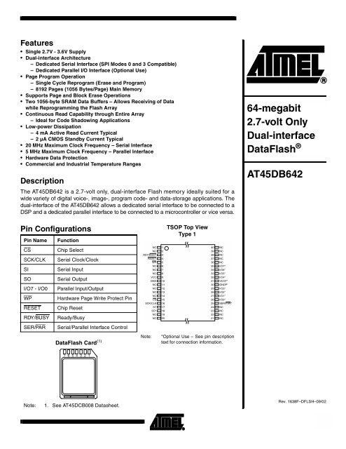
However, the use of either <strong>interface</strong> is purely optional. Its 69,206,016 bits of memory are organizedas 8192 pages of 1056 bytes each. In addition to the main memory, the AT45DB<strong>64</strong>2also contains two SRAM data buffers of 1056 bytes each. The buffers allow receiving of datawhile a page in the main memory is being reprogrammed, as well as reading or writing a continuousdata stream. EEPROM emulation (bit or byte alterability) is easily handled with a selfcontainedthree step Read-Modify-Write operation. Unlike conventional Flash memories thatare accessed randomly with multiple address lines and a parallel <strong>interface</strong>, the <strong>DataFlash</strong> ®uses either a serial <strong>interface</strong> or a parallel <strong>interface</strong> to sequentially access its data. The simplesequential access facilitates hardware layout, increases system reliability, minimizes switchingnoise, and reduces package size and active pin count. <strong>DataFlash</strong> supports SPI mode 0 andmode 3. The device is optimized for use in many commercial and industrial applications wherehigh-density, low-pin count, low-<strong>volt</strong>age, and low-power are essential. The device operates atclock frequencies up to 20 MHz with a typical active read current consumption of 4 mA.To allow for simple in-system reprogrammability, the AT45DB<strong>64</strong>2 does not require high input<strong>volt</strong>ages for programming. The device operates from a single power supply, <strong>2.7</strong>V to 3.6V, forboth the program and read operations. The AT45DB<strong>64</strong>2 is enabled through the chip select pin(CS) and accessed via a three-wire <strong>interface</strong> consisting of the Serial Input (SI), Serial Output(SO), and the Serial Clock (SCK), or a parallel <strong>interface</strong> consisting of the parallel input/outputpins (I/O7 - I/O0) and the clock pin (CLK). The SCK and CLK pins are shared and provide thesame clocking input to the <strong>DataFlash</strong>.All programming cycles are self-timed, and no separate erase cycle is required beforeprogramming.When the device is shipped from Atmel, the most significant page of the memory array maynot be erased. In other words, the contents of the last page may not be filled with FFH.Block DiagramWPFLASH MEMORY ARRAYPAGE (1056 BYTES)BUFFER 1 (1056 BYTES)BUFFER 2 (1056 BYTES)SCK/CLKCSRESETVCCGNDRDY/BUSYSER/PARSISOI/O INTERFACEI/O7 - I/O0Memory ArrayTo provide optimal flexibility, the memory array of the AT45DB<strong>64</strong>2 is divided into three levelsof granularity comprising of sectors, blocks and pages. The “Memory Architecture Diagram”illustrates the breakdown of each level and details the number of pages per sector and block.All program operations to the <strong>DataFlash</strong> occur on a page-by-page basis; however, the optionalerase operations can be performed at the block or page level.2 AT45DB<strong>64</strong>21638F–DFLSH–09/02
CONTINUOUS ARRAY READ: By supplying an initial starting address for the main memoryarray, the Continuous Array Read command can be utilized to sequentially read a continuousstream of data from the device by simply providing a clock signal; no additional addressinginformation or control signals need to be provided. The <strong>DataFlash</strong> incorporates an internaladdress counter that will automatically increment on every clock cycle, allowing one continuousread operation without the need of additional address sequences. To perform acontinuous read, an opcode of 68H or E8H must be clocked into the device followed by threeaddress bytes (which comprise the 24-bit page and byte address sequence) and a series ofdon’t care bytes (four don’t care bytes if using the serial <strong>interface</strong> or 60 don’t care bytes ifusing the parallel <strong>interface</strong>). The first 13 bits (PA12 - PA0) of the 24-bit (three byte) addresssequence specify which page of the main memory array to read, and the last 11 bits (BA10 -BA0) of the 24-bit address sequence specify the starting byte address within the page. Thefour or 60 don’t care bytes that follow the three address bytes are needed to initialize the readoperation. Following the don’t care bytes, additional clock pulses on the SCK/CLK pin willresult in data being output on either the SO (serial output) pin or the parallel output pins (I/O7-I/O0).The CS pin must remain low during the loading of the opcode, the address bytes, the don’tcare bytes, and the reading of data. When the end of a page in main memory is reached duringa Continuous Array Read, the device will continue reading at the beginning of the nextpage with no delays incurred during the page boundary crossover (the crossover from the endof one page to the beginning of the next page). When the last bit (or byte if using the parallel<strong>interface</strong> mode) in the main memory array has been read, the device will continue readingback at the beginning of the first page of memory. As with crossing over page boundaries, nodelays will be incurred when wrapping around from the end of the array to the beginning of thearray.A low-to-high transition on the CS pin will terminate the read operation and tri-state the outputpins (SO or I/O7-I/O0). The maximum SCK/CLK frequency allowable for the Continuous ArrayRead is defined by the f CAR specification. The Continuous Array Read bypasses both databuffers and leaves the contents of the buffers unchanged.BURST ARRAY READ WITH SYNCHRONOUS DELAY: The Burst Array Read with SynchronousDelay functions very similarly to the Continuous Array Read operation but allows muchhigher read throughputs by utilizing faster clock frequencies. It incorporates a synchronousdelay (through the use of don't care clock cycles) when crossing over page boundaries. Toperform a Burst Array Read with Synchronous Delay, an opcode of 69H or E9H must beclocked into the device followed by three address bytes (which comprise the 24-bit page andbyte address sequence) and a series of don't care bytes (four don't care bytes if using theserial <strong>interface</strong> or 60 don't care bytes if using the parallel <strong>interface</strong>). The first 13 bits (PA12-PA0) of the 24-bit (three byte) address sequence specify which page of the main memoryarray to read, and the last 11 bits (BA10-BA0) of the 24-bit address sequence specify the startingbyte address within the page. The don't care bytes that follow the three address bytes areneeded to initialize the read operation. Following the don't care bytes, additional clock pulseson the SCK/CLK pin will result in data being output on either the SO pin or the I/O7-I/O0 pins.4 AT45DB<strong>64</strong>21638F–DFLSH–09/02
AT45DB<strong>64</strong>2As with the Continuous Array Read, the CS pin must remain low during the loading of theopcode, the address bytes, the don't care bytes, and the reading of data. During a Burst ArrayRead with Synchronous Delay, when the end of a page in main memory is reached (the last bitor the last byte of the page has been clocked out), the system must send an additional 32don't care clock cycles before the first bit (or byte if using the parallel <strong>interface</strong> mode) of thenext page can be read out. These 32 don't care clock cycles are necessary to allow the deviceenough time to cross over the burst read boundary (the crossover from the end of one page tothe beginning of the next page). By utilizing the 32 don't care clock cycles, the system doesnot need to delay the SCK/CLK signal to the device which allows synchronous operation whenreading multiple pages of the memory array. Please see the detailed read timing waveformsfor illustrations (beginning on page 21) on which clock cycle data will actually begin to beoutput.When the last bit (or byte in the parallel <strong>interface</strong> mode) in the main memory array has beenread, the device will continue reading back at the beginning of the first page of memory. Thetransition from the last bit (or byte when using the parallel <strong>interface</strong>) of the array back to thebeginning of the array is also considered a burst read boundary. Therefore, the system mustsend 32 don't care clock cycles before the first bit (or byte if using the parallel <strong>interface</strong> mode)of the memory array can be read.A low-to-high transition on the CS pin will terminate the read operation and tri-state the outputpins (SO or I/O7-I/O0). The maximum SCK/CLK frequency allowable for the Burst Array Readwith Synchronous Delay is defined by the f BARSD specification. The Burst Array Read with SynchronousDelay bypasses both data buffers and leaves the contents of the buffers unchanged.MAIN MEMORY PAGE READ: A main memory page read allows the user to read datadirectly from any one of the 8192 pages in the main memory, bypassing both of the data buffersand leaving the contents of the buffers unchanged. To start a page read, an opcode of 52Hor D2H must be clocked into the device followed by three address bytes (which comprise the24-bit page and byte address sequence) and a series of don’t care bytes (four don’t carebytesif using the serial <strong>interface</strong> or 60 don’t care bytes if the using parallel <strong>interface</strong>). The first 13bits (PA12 - PA0) of the 24-bit (three-byte) address sequence specify the page in main memoryto be read, and the last 11 bits (BA10 - BA0) of the 24-bit address sequence specify thestarting byte address within that page. The four or 60 don’t care bytes that follow the threeaddress bytes are sent to initialize the read operation. Following the don’t carebytes,additionalpulses on SCK/CLK result in data being output on either the SO (serial output) pin or theparallel output pins (I/O7 - I/O0). The CS pin must remain low during the loading of theopcode, the address bytes, the don’t care bytes, and the reading of data. When the end of apage in main memory is reached, the device will continue reading back at the beginning of thesame page. A low-to-high transition on the CS pin will terminate the read operation and tristatethe output pins (SO or I/O7 - I/O0).BUFFER READ: Data can be read from either one of the two buffers, using different opcodesto specify which buffer to read from. An opcode of 54H or D4H is used to read data from buffer1, and an opcode of 56H or D6H is used to read data from buffer 2. To perform a buffer read,the opcode must be clocked into the device followed by three address bytes comprised of 13don’t care bits and 11 buffer address bits (BFA10 - BFA0). Following the three address bytes,an additional don’t care byte must be clocked in to initialize the read operation. Since thebuffer size is 1056 bytes, 11 buffer address bits are required to specify the first byte of data tobe read from the buffer. The CS pin must remain low during the loading of the opcode, theaddress bytes, the don’t care bytes, and the reading of data. When the end of a buffer isreached, the device will continue reading back at the beginning of the buffer. A low-to-hightransition on the CS pin will terminate the read operation and tri-state the output pins (SO orI/O7 - I/O0).1638F–DFLSH–09/025
STATUS REGISTER READ: The status register can be used to determine the device’sready/busy status, the result of a Main Memory Page to Buffer Compare operation, or thedevice density. To read the status register, an opcode of 57H or D7H must be loaded into thedevice. After the opcode is clocked in, the 1-byte status register will be clocked out on the outputpins (SO or I/O7 - I/O0), starting with the next clock cycle. When using the serial <strong>interface</strong>,the data in the status register, starting with the MSB (bit 7), will be clocked out on the SO pinduring the next eight clock cycles.The five most-significant bits of the status register will contain device information, while theremaining three least-significant bits are reserved for future use and will have undefined values.After the one byte of the status register has been clocked out, the sequence will repeatitself (as long as CS remains low and SCK/CLK is being toggled). The data in the status registeris constantly updated, so each repeating sequence will output new data.Ready/busy status is indicated using bit 7 of the status register. If bit 7 is a 1, then the deviceis not busy and is ready to accept the next command. If bit 7 is a 0, then the device is in a busystate. The user can continuously poll bit 7 of the status register by stopping SCK/CLK at a lowlevel once bit 7 has been output on the SO or I/O7 pin. The status of bit 7 will continue to beoutput on the SO or I/O7 pin, and once the device is no longer busy, the state of the SO orI/O7 pin will change from 0 to 1. There are eight operations that can cause the device to be ina busy state: Main Memory Page to Buffer Transfer, Main Memory Page to Buffer Compare,Buffer to Main Memory Page Program with Built-in Erase, Buffer to Main Memory Page Programwithout Built-in Erase, Page Erase, Block Erase, Main Memory Page Program, and AutoPage Rewrite.The result of the most recent Main Memory Page to Buffer Compare operation is indicatedusing bit 6 of the status register. If bit 6 is a 0, then the data in the main memory page matchesthe data in the buffer. If bit 6 is a 1, then at least one bit of the data in the main memory pagedoes not match the data in the buffer.The device density is indicated using bits 5, 4, 3 and 2 of the status register. For theAT45DB<strong>64</strong>2, the four bits are logical “1”s. The decimal value of these four binary bits does notequate to the device density; the four bits represent a combinational code relating to differingdensities of <strong>DataFlash</strong> devices, allowing a total of sixteen different density configurations.Status Register FormatBit 7 Bit 6 Bit 5 Bit 4 Bit 3 Bit 2 Bit 1 Bit 0RDY/BUSY COMP 1 1 1 1 X XProgram andErase CommandsBUFFER WRITE: Data can be clocked in from the input pins (SI or I/O7 - I/O0) into eitherbuffer 1 or buffer 2. To load data into either buffer, a 1-byte opcode, 84H for buffer 1 or 87H forbuffer 2, must be clocked into the device, followed by three address bytes comprised of 13don’t care bits and 11 buffer address bits (BFA10 - BFA0). The 11 buffer address bits specifythe first byte in the buffer to be written. After the last address byte has been clocked into thedevice, data can then be clocked in on subsequent clock cycles. If the end of the data buffer isreached, the device will wrap around back to the beginning of the buffer. Data will continue tobe loaded into the buffer until a low-to-high transition is detected on the CS pin.6 AT45DB<strong>64</strong>21638F–DFLSH–09/02
AT45DB<strong>64</strong>2BUFFER TO MAIN MEMORY PAGE PROGRAM WITH BUILT-IN ERASE: Data written intoeither buffer 1 or buffer 2 can be programmed into the main memory. A 1-byte opcode, 83H forbuffer 1 or 86H for buffer 2, must be clocked into the device followed by three address bytesconsisting of 13 page address bits (PA12 - PA0) that specify the page in the main memory tobe written and 11 don’t care bits. When a low-to-high transition occurs on the CS pin, the partwill first erase the selected page in main memory (the erased state is a logical 1) and then programthe data stored in the buffer into the specified page in main memory. Both the erase andthe programming of the page are internally self-timed and should take place in a maximumtime of t EP . During this time, the status register and the RDY/BUSY pin will indicate that thepart is busy.BUFFER TO MAIN MEMORY PAGE PROGRAM WITHOUT BUILT-IN ERASE: A previouslyerasedpage within main memory can be programmed with the contents of either buffer 1 orbuffer 2. A 1-byte opcode, 88H for buffer 1 or 89H for buffer 2, must be clocked into the devicefollowed by three address bytes consisting of 13 page address bits (PA12 - PA0) that specifythe page in the main memory to be written and 11 don’t care bits. When a low-to-high transitionoccurs on the CS pin, the part will program the data stored in the buffer into the specifiedpage in the main memory. It is necessary that the page in main memory that is being programmedhas been previously erased using one of the optional erase commands (Page Eraseor Block Erase). The programming of the page is internally self-timed and should take place ina maximum time of t P . During this time, the status register and the RDY/BUSY pin will indicatethat the part is busy.Successive page programming operations, without doing a page erase, are not recommended.In other words, changing bytes within a page from a “1” to a “0” during multiple pageprogramming operations without erasing that page is not recommended.PAGE ERASE: The optional Page Erase command can be used to individually erase anypage in the main memory array allowing the Buffer to Main Memory Page Program withoutBuilt-in Erase command to be utilized at a later time. To perform a page erase, an opcode of81H must be loaded into the device, followed by three address bytes comprised of 13 pageaddress bits (PA12 - PA0) and 11 don’t care bits. The 13 page address bits are used to specifywhich page of the memory array is to be erased. When a low-to-high transition occurs onthe CS pin, the part will erase the selected page (the erased state is a logical 1). The eraseoperation is internally self-timed and should take place in a maximum time of t PE . During thistime, the status register and the RDY/BUSY pin will indicate that the part is busy.BLOCK ERASE: A block of eight pages can be erased at one time allowing the Buffer to MainMemory Page Program without Built-in Erase command to be utilized to reduce programmingtimes when writing large amounts of data to the device. To perform a block erase, an opcodeof 50H must be loaded into the device, followed by three address bytes comprised of 10 pageaddress bits (PA12 -PA3) and 14 don’t care bits. The 10 page address bits are used to specifywhich block of eight pages is to be erased. When a low-to-high transition occurs on the CSpin, the part will erase the selected block of eight pages. The erase operation is internally selftimedand should take place in a maximum time of t BE . During this time, the status register andthe RDY/BUSY pin will indicate that the part is busy.1638F–DFLSH–09/027
AT45DB<strong>64</strong>2MAIN MEMORY PAGE TO BUFFER COMPARE: A page of data in main memory can becompared to the data in buffer 1 or buffer 2. To initiate the operation, a 1-byte opcode, 60H forbuffer 1 and 61H for buffer 2, must be clocked into the device, followed by three address bytesconsisting of 13 page address bits (PA12 - PA0) that specify the page in the main memory thatis to be compared to the buffer, and 11 don’t carebits.TheCSpin must be low while togglingthe SCK/CLK pin to load the opcode and the address bytes from the input pins (SI or I/O7 -I/O0). On the low-to-high transition of the CS pin, the 1056 bytes in the selected main memorypage will be compared with the 1056 bytes in buffer 1 or buffer 2. During this time (t XFR ), thestatus register and the RDY/BUSY pin will indicate that the part is busy. On completion of thecompare operation, bit 6 of the status register is updated with the result of the compare.AUTO PAGE REWRITE: This mode is only needed if multiple bytes within a page or multiplepages of data are modified in a random fashion. This mode is a combination of two operations:Main Memory Page to Buffer Transfer and Buffer to Main Memory Page Program with Built-inErase. A page of data is first transferred from the main memory to buffer 1 or buffer 2, andthen the same data (from buffer 1 or buffer 2) is programmed back into its original page ofmain memory. To start the rewrite operation, a 1-byte opcode, 58H for buffer 1 or 59H forbuffer 2, must be clocked into the device, followed by three address bytes comprised of 13page address bits (PA12 - PA0) that specify the page in main memory to be rewritten and 11don’t care bits. When a low-to-high transition occurs on the CS pin, the part will first transferdata from the page in main memory to a buffer and then program the data from the buffer backinto same page of main memory. The operation is internally self-timed and should take placein a maximum time of t EP . During this time, the status register and the RDY/BUSY pin will indicatethat the part is busy.If a sector is programmed or reprogrammed sequentially page by page, then the programmingalgorithm shown in Figure 1 (page 33) is recommended. Otherwise, if multiple bytes in a pageor several pages are programmed randomly in a sector, then the programming algorithmshown in Figure 2 (page 34) is recommended. Each page within a sector must beupdated/rewritten at least once within every 10,000 cumulative page erase/program operationsin that sector.Operation ModeSummaryThe modes described can be separated into two groups – modes that make use of the Flashmemory array (Group A) and modes that do not make use of the Flash memory array(Group B).Group A modes consist of:1. Main Memory Page to Buffer 1 (or 2) Transfer2. Main Memory Page to Buffer 1 (or 2) Compare3. Buffer 1 (or 2) to Main Memory Page Program with Built-in Erase4. Buffer 1 (or 2) to Main Memory Page Program without Built-in Erase5. Page Erase6. Block Erase7. Main Memory Page Program through Buffer8. Auto Page Rewrite9. Group B modes consist of:10. Buffer 1 (or 2) Read11. Buffer 1 (or 2) Write12. Status Register ReadIf a Group A mode is in progress (not fully completed), then another mode in Group A shouldnot be started. However, during this time in which a Group A mode is in progress, modes inGroup B can be started.1638F–DFLSH–09/029
This gives the <strong>DataFlash</strong> the ability to virtually accommodate a continuous data stream. Whiledata is being programmed into main memory from buffer 1, data can be loaded into buffer 2(or vice versa). See application note AN-4 (“Using Atmel’s Serial <strong>DataFlash</strong>”) for more details.Pin DescriptionsSERIAL/PARALLEL INTERFACE CONTROL (SER/PAR): The <strong>DataFlash</strong> may be configuredto utilize either its serial port or parallel port through the use of the serial/parallel control pin(SER/PAR). The <strong>Dual</strong> Interface offers more flexibility in a system design with both the serialand parallel modes offered on the same device. When the SER/PAR pin is held high, the serialport (SI and SO) of the <strong>DataFlash</strong> will be used for all data transfers, and the parallel port(I/O7 - I/O0) will be in a high impedance state. Any data presented on the parallel port whileSER/PAR is held high will be ignored. When the SER/PAR is held low, the parallel port will beused for all data transfers, and the SO pin of the serial port will be in a high impedance state.While SER/PAR is low, any data presented on the SI pin will be ignored. Switching betweenthe serial port and parallel port can be done at anytime provided the following conditions aremet: 1) CS should be held high during the switching between the two modes. 2) T SPH(SER/PAR hold time) and T SPS (SER/PAR Setup time) requirements should be followed.Having both a serial port and a parallel port on the <strong>DataFlash</strong> allows the device to reside ontwo buses that can be connected to different processors. The advantage of switching betweenthe serial and parallel port is that while an internally self-timed operation such as an erase orprogram operation is started with either port, a simultaneous operation such as a buffer reador buffer write can be started utilizing the other port.The SER/PAR pin is internally pulled high; therefore, if the parallel port is never to be used,then connection of the SER/PAR pin is not necessary. In addition, if the SER/PAR pin is notconnected or if the SER/PAR pin is always driven high externally, then the parallel input/outputpins (I/O7-I/O0), the VCCP pin, and the GNDP pin should be treated as “don’t connects.”SERIAL INPUT (SI): The SI pin is an input-only pin and is used to shift data serially into thedevice. The SI pin is used for all data input, including opcodes and address sequences. If theSER/PAR pin is always driven low, then the SI pin should be a “don’t connect”.SERIAL OUTPUT (SO): The SO pin is an output-only pin and is used to shift data serially outfrom the device. If the SER/PAR pin is always driven low, then the SO pin should be a “don’tconnect”.PARALLEL INPUT/OUTPUT (I/O7-I/O0): The I/O7-I/O0 pins are bidirectional and used toclock data into and out of the device. The I/O7-I/O0 pins are used for all data input, includingopcodes and address sequences. The use of these pins is optional, and the pins should betreated as “don’t connects” if the SER/PAR pin is not connected or if the SER/PAR pin isalways driven high externally.SERIAL CLOCK/CLOCK (SCK/CLK): The SCK/CLK pin is an input-only pin and is used tocontrol the flow of data to and from the <strong>DataFlash</strong>. Data is always clocked into the device onthe rising edge of SCK/CLK and clocked out of the device on the falling edge of SCK/CLK.CHIP SELECT (CS): The <strong>DataFlash</strong> is selected when the CS pin is low. When the device isnot selected, data will not be accepted on the input pins (SI or I/O7-I/O0), and the output pins(SO or I/O7-I/O0) will remain in a high impedance state. A high-to-low transition on the CS pinis required to start an operation, and a low-to-high transition on the CS pinisrequiredtoendan operation.HARDWARE PAGE WRITE PROTECT: If the WP pin is held low, the first 256 pages (sectors0 and 1) of the main memory cannot be reprogrammed. The only way to reprogram the first256 pages is to first drive the protect pin high and then use the program commands previouslymentioned. The WP pin is internally pulled high; therefore, in low pin count applications, connectionof the WP pin is not necessary if this pin and feature will not be utilized. However, it isrecommended that the WP pin be driven high externally whenever possible.10 AT45DB<strong>64</strong>21638F–DFLSH–09/02
AT45DB<strong>64</strong>2RESET: Alowstateontheresetpin(RESET) will terminate the operation in progress andreset the internal state machine to an idle state. The device will remain in the reset conditionas long as a low level is present on the RESET pin. Normal operation can resume once theRESET pin is brought back to a high level.The device incorporates an internal power-on reset circuit, so there are no restrictions on theRESET pin during power-on sequences. The RESET pin is also internally pulled high; therefore,in low pin count applications, connection of the RESET pin is not necessary if this pin andfeature will not be utilized. However, it is recommended that the RESET pinbedrivenhighexternally whenever possible.READY/BUSY: This open drain output pin will be driven low when the device is busy in aninternally self-timed operation. This pin, which is normally in a high state (through an externalpull-up resistor), will be pulled low during programming/erase operations, compare operations,and page-to-buffer transfers.The busy status indicates that the Flash memory array and one of the buffers cannot beaccessed; read and write operations to the other buffer can still be performed.PARALLEL PORT SUPPLY VOLTAGE (VCCP AND GNDP): The VCCP and GNDP pins areused to supply power for the parallel input/output pins (I/O7-I/O0). The VCCP and GNDP pinsneed to be used if the parallel port is to be utilized; however, these pins should be treated as“don’t connects” if the SER/PAR pin is not connected or if the SER/PAR pin is always drivenhigh externally.Power-on/ResetStateSystemConsiderationsWhen power is first applied to the device, or when recovering from a reset condition, thedevice will default to SPI Mode 3 or Inactive Clock Polarity High. In addition, the output pins(SO or I/O7 - I/O0) will be in a high impedance state, and a high-to-low transition on the CS pinwill be required to start a valid instruction. The SPI mode or the clock polarity mode will beautomatically selected on every falling edge of CS by sampling the inactive Clock State.The SPI <strong>interface</strong> is controlled by the serial clock SCK, serial input SI and chip select CS pins.The sequential 8-bit parallel <strong>interface</strong> is controlled by the clock CLK, 8 I/Os and chip select CSpins. These signals must rise and fall monotonically and be free from noise. Excessive noiseor ringing on these pins can be misinterpreted as multiple edges and cause improper operationof the device. The PC board traces must be kept to a minimum distance or appropriatelyterminated to ensure proper operation. If necessary, decoupling capacitors can be added onthese pins to provide filtering against noise glitches.As system complexity continues to increase, <strong>volt</strong>age regulation is becoming more important. Akey element of any <strong>volt</strong>age regulation scheme is its current sourcing capability. Like all Flashmemories, the peak current for <strong>DataFlash</strong> occur during the programming and erase operation.The regulator needs to supply this peak current requirement. An under specified regulator cancause current starvation. Besides increasing system noise, current starvation during programmingor erase can lead to improper operation and possible data corruption.1638F–DFLSH–09/0211
Table 1. Read CommandsCommand SCK/CLK Mode OpcodeContinuous Array ReadBurst Array Read with Synchronous DelayMain Memory Page ReadBuffer 1 ReadBuffer 2 ReadStatus Register ReadInactive Clock Polarity Low or HighSPI Mode 0 or 3Inactive Clock Polarity Low or HighSPI Mode 0 or 3Inactive Clock Polarity Low or HighSPI Mode 0 or 3Inactive Clock Polarity Low or HighSPI Mode 0 or 3Inactive Clock Polarity Low or HighSPI Mode 0 or 3Inactive Clock Polarity Low or HighSPI Mode 0 or 368HE8H69HE9H52HD2H54HD4H56HD6H57HD7HTable 2. Program and Erase CommandsCommand SCK/CLK Mode OpcodeBuffer 1 Write Any 84HBuffer 2 Write Any 87HBuffer 1 to Main Memory Page Program with Built-in Erase Any 83HBuffer 2 to Main Memory Page Program with Built-in Erase Any 86HBuffer 1 to Main Memory Page Program without Built-in Erase Any 88HBuffer 2 to Main Memory Page Program without Built-in Erase Any 89HPage Erase Any 81HBlock Erase Any 50HMain Memory Page Program Through Buffer 1 Any 82HMain Memory Page Program Through Buffer 2 Any 85HTable 3. Additional CommandsCommand SCK/CLK Mode OpcodeMain Memory Page to Buffer 1 Transfer Any 53HMain Memory Page to Buffer 2 Transfer Any 55HMain Memory Page to Buffer 1 Compare Any 60HMain Memory Page to Buffer 2 Compare Any 61HAuto Page Rewrite Through Buffer 1 Any 58HAuto Page Rewrite Through Buffer 2 Any 59HNote:In Tables 2 and 3, an SCK/CLK mode designation of “Any” denotes any one of the four modes of operation (Inactive ClockPolarity Low, Inactive Clock Polarity High, SPI Mode 0, or SPI Mode 3).12 AT45DB<strong>64</strong>21638F–DFLSH–09/02
AT45DB<strong>64</strong>2Table 4. Detailed Bit-level Addressing SequenceAdditionalDon’t CareBytesOpcode OpcodeRequired50H 0 1 0 1 0 0 0 0 P P P P P P P P P P x x x x x x x x x x x x x x N/ANote:PA12PA11P = Page Address BitB = Byte/Buffer Address Bitx=Don’t Care* 4 Bytes for Serial Interface60 Bytes for Parallel InterfaceAddress Byte Address Byte Address BytePA10PA9PA8PA7PA6PA5PA452H 0 1 0 1 0 0 1 0 P P P P P P P P P P P P P B B B B B B B B B B B4or60Bytes*53H 0 1 0 1 0 0 1 1 P P P P P P P P P P P P P x x x x x x x x x x x N/A54H 0 1 0 1 0 1 0 0 x x x x x x x x x x x x x B B B B B B B B B B B 1Byte55H 0 1 0 1 0 1 0 1 P P P P P P P P P P P P P x x x x x x x x x x x N/A56H 0 1 0 1 0 1 1 0 x x x x x x x x x x x x x B B B B B B B B B B B 1Byte57H 0 1 0 1 0 1 1 1 N/A N/A N/A N/A58H 0 1 0 1 1 0 0 0 P P P P P P P P P P P P P x x x x x x x x x x x N/A59H 0 1 0 1 1 0 0 1 P P P P P P P P P P P P P x x x x x x x x x x x N/A60H 0 1 1 0 0 0 0 0 P P P P P P P P P P P P P x x x x x x x x x x x N/A61H 0 1 1 0 0 0 0 1 P P P P P P P P P P P P P x x x x x x x x x x x N/A68H 0 1 1 0 1 0 0 0 P P P P P P P P P P P P P B B B B B B B B B B B4or60Bytes*69H 0 1 1 0 1 0 0 1 P P P P P P P P P P P P P B B B B B B B B B B B4or60Bytes*81H 1 0 0 0 0 0 0 1 P P P P P P P P P P P P P x x x x x x x x x x x N/A82H 1 0 0 0 0 0 1 0 P P P P P P P P P P P P P B B B B B B B B B B B N/A83H 1 0 0 0 0 0 1 1 P P P P P P P P P P P P P x x x x x x x x x x x N/A84H 1 0 0 0 0 1 0 0 x x x x x x x x x x x x x B B B B B B B B B B B N/A85H 1 0 0 0 0 1 0 1 P P P P P P P P P P P P P B B B B B B B B B B B N/A86H 1 0 0 0 0 1 1 0 P P P P P P P P P P P P P x x x x x x x x x x x N/A87H 1 0 0 0 0 1 1 1 x x x x x x x x x x x x x B B B B B B B B B B B N/A88H 1 0 0 0 1 0 0 0 P P P P P P P P P P P P P x x x x x x x x x x x N/A89H 1 0 0 0 1 0 0 1 P P P P P P P P P P P P P x x x x x x x x x x x N/AD2H 1 1 0 1 0 0 1 0 P P P P P P P P P P P P P B B B B B B B B B B B4or60Bytes*D4H 1 1 0 1 0 1 0 0 x x x x x x x x x x x x x B B B B B B B B B B B 1ByteD6H 1 1 0 1 0 1 1 0 x x x x x x x x x x x x x B B B B B B B B B B B 1ByteD7H 1 1 0 1 0 1 1 1 N/A N/A N/A N/AE8H 1 1 1 0 1 0 0 0 P P P P P P P P P P P P P B B B B B B B B B B BE9H 1 1 1 0 1 0 0 1 P P P P P P P P P P P P P B B B B B B B B B B BPA3PA2PA1PA0BA10BA9BA8BA7BA6BA5BA4BA3BA2BA1BA04or60Bytes*4or60Bytes*1638F–DFLSH–09/0213
Absolute Maximum Ratings*Temperature under Bias ................................ -55°C to+125°CStorage Temperature ..................................... -65°C to+150°CAll Input Voltages(including NC Pins)with Respect to Ground ...................................-0.6V to +6.25VAll Output Voltageswith Respect to Ground .............................-0.6V to V CC +0.6V*NOTICE: Stresses beyond those listed under “AbsoluteMaximum Ratings” may cause permanent damageto the device. This is a stress rating only andfunctional operation of the device at these or anyother conditions beyond those indicated in theoperational sections of this specification is notimplied. Exposure to absolute maximum ratingconditions for extended periods may affectdevice reliability.DC and AC Operating RangeOperating Temperature (Case)Com.Ind.Note: 1. After power is applied and V CC is at the minimum specified datasheet value, the system should wait 20 ms before an operationalmode is started.Notes: 1. I CC1 during a buffer read is 20 mA maximum.2. I CC2 during a buffer read is 25 mA maximum.AT45DB<strong>64</strong>20°C to70°C-40°C to85°CV CC Power Supply (1) <strong>2.7</strong>V to 3.6VDC CharacteristicsSymbol Parameter Condition Min Typ Max UnitsI SBI CC1(1)I CC2(2)I CC3I CC4I CC5Standby CurrentActive Current, ReadOperation, Serial InterfaceActive Current, ReadOperation, Parallel InterfaceActive Current, ProgramOperation, Page ProgramActive Current, ProgramOperation, Fast Page ProgramActive Current, EraseOperation, PageCS, RESET, WP=V IH ,allinputs at CMOS levelsf=20MHz;I OUT =0mA;V CC =3.6Vf=5MHz;I OUT =0mA;V CC =3.6V2 10 µA4 10 mA8 15 mAV CC =3.6V 20 35 mAV CC =3.6V 30 50 mAV CC =3.6V 20 35 mAI CC6Active Current, EraseOperation, BlockV CC =3.6V 20 35 mAI LI Input Load Current V IN =CMOSlevels 1 µAI LO Output Leakage Current V I/O = CMOS levels 1 µAV IL Input Low Voltage 0.6 VV IH Input High Voltage 2.0 VV OL Output Low Voltage I OL =1.6mA;V CC =<strong>2.7</strong>V 0.4 VV OH Output High Voltage I OH =-100µA V CC -0.2V V14 AT45DB<strong>64</strong>21638F–DFLSH–09/02
AT45DB<strong>64</strong>2AC Characteristics – Serial/Parallel InterfaceSymbol Parameter Min Max Unitst SPH SER/PAR Hold Time 100 nst SPS SER/PAR Setup Time 100 nsAC Characteristics – Serial InterfaceSymbol Parameter Min Max Unitsf SCK SCK Frequency 20 MHzf CAR SCK Frequency for Continuous Array Read 15 MHzf BARSD SCK Frequency for Burst Array Read with Synchronous Delay 20 MHzt WH SCK High Time 22 nst WL SCK Low Time 22 nst CS Minimum CS High Time 250 nst CSS CS Setup Time 250 nst CSH CS Hold Time 250 nst CSB CS High to RDY/BUSY Low 150 nst SU Data In Setup Time 5 nst H Data In Hold Time 10 nst HO Output Hold Time 0 nst DIS Output Disable Time 18 nst V Output Valid 20 nst XFR Page to Buffer Transfer/Compare Time 700 µst EP Page Erase and Programming Time 20 mst P Page Programming Time 14 mst PE Page Erase Time 8 mst BE Block Erase Time 12 mst RST RESET Pulse Width 10 µst REC RESET Recovery Time 1 µs1638F–DFLSH–09/0215
AC Characteristics – Parallel InterfaceSymbol Parameter Min Max Unitsf SCK1 CLK Frequency 5 MHzf CAR1 CLK Frequency for Continuous Array Read 3 MHzf BARSD1 CLK Frequency for Burst Array Read with Synchronous Delay 5 MHzt WH CLK High Time 80 nst WL CLK Low Time 80 nst CS Minimum CS High Time 250 nst CSS CS Setup Time 250 nst CSH CS Hold Time 250 nst CSB CS High to RDY/BUSY Low 150 nst SU Data In Setup Time 75 nst H Data In Hold Time 25 nst HO Output Hold Time 0 nst DIS Output Disable Time 55 nst V Output Valid 70 nst XFR Page to Buffer Transfer/Compare Time 700 µst EP Page Erase and Programming Time 20 mst P Page Programming Time 14 mst PE Page Erase Time 8 mst BE Block Erase Time 12 mst RST RESET Pulse Width 10 µst REC RESET Recovery Time 1 µsTest Waveforms and Measurement LevelsACDRIVINGLEVELS2.4V0.45V2.00.8ACMEASUREMENTLEVELtR, tF < 3 ns (10% to 90%)Output Test LoadDEVICEUNDERTEST30 pF16 AT45DB<strong>64</strong>21638F–DFLSH–09/02
AT45DB<strong>64</strong>2AC WaveformsTwo different timing diagrams are shown below. Waveform 1 shows the SCK/CLK signalbeing low when CS makes a high-to-low transition, and Waveform 2 shows the SCK/CLK signalbeing high when CS makes a high-to-low transition. Both waveforms show valid timingdiagrams. The setup and hold times for the input signals (SI or I/O7-I/O0) are referenced to thelow-to-high transition on the SCK/CLK signal.Waveform 1 shows timing that is also compatible with SPI Mode 0, and Waveform 2 showstiming that is compatible with SPI Mode 3.Waveform 1 –Inactive ClockPolarity Low andSPI Mode 0CStCSStWH tWL tCSHtCSSCK/CLKSO or I/O7 - I/O0(OUTPUT)HIGH IMPEDANCEtSUtVtHtHOVALID OUTtDISHIGH IMPEDANCESI or I/O7 - I/O0(INPUT)VALID INWaveform 2 –Inactive ClockPolarity High andSPI Mode 3CStCSStWL tWH tCSHtCSSCK/CLKSO or I/O7 - I/O0(OUTPUT)tVHIGH ZtSUtHOVALID OUTtHtDISHIGH IMPEDANCESI or I/O7 - I/O0(INPUT)VALID IN171638F–DFLSH–09/02
Reset Timing (Inactive Clock Polarity Low Shown)CStRECtCSSSCK/CLKtRSTRESETSO or I/O7 - I/O0(OUTPUT)SI or I/O7 - I/O0(INPUT)HIGH IMPEDANCEHIGH IMPEDANCENote:The CS signal should be in the high state before the RESET signal is deasserted.Serial/Parallel Interface TimingCSSER/PARt SPHt SPSCommand Sequence for Read/Write Operations (Except Status Register Read)SI or I/O7 - I/O0(INPUT)CMD 8 bits 8 bits 8 bitsMSBX X X XX X X XX X X X X X X X X X X X X X X XLSBPage Address(PA12 - PA0)Byte/Buffer Address(BA10 - BA0/BFA10 - BFA0)18 AT45DB<strong>64</strong>21638F–DFLSH–09/02
AT45DB<strong>64</strong>2Write OperationsThe following block diagram and waveforms illustrate the various write sequences available.FLASH MEMORY ARRAYPAGE (1056 BYTES)BUFFER 1 TOMAIN MEMORYPAGE PROGRAMBUFFER 1 (1056 BYTES)BUFFER 1WRITEMAIN MEMORYPAGE PROGRAMTHROUGH BUFFER 2MAIN MEMORY PAGEPROGRAM THROUGHBUFFER 1I/O INTERFACEBUFFER 2 TOMAIN MEMORYPAGE PROGRAMBUFFER 2 (1056 BYTES)BUFFER 2WRITESII/O7 - I/O0Main Memory Page Program through Buffers· Completes writing into selected buffer· Starts self-timed erase/program operationCSSI or I/O7 - I/O0(INPUT)CMD PA12-5 PA4-0, BFA10-8 BFA7-0n n+1 Last ByteBuffer Write· Completes writing into selected bufferCSSI or I/O7 - I/O0(INPUT)CMD X X···X, BFA10-8 BFA7-0 n n+1 Last ByteBuffer to Main Memory Page Program (Data from Buffer Programmed into Flash Page)CSStarts self-timed erase/program operationSI or I/O7 - I/O0(INPUT)CMD PA12-5 PA4-0, XXXX···XEach transitionrepresents 8 bitsn=1stbytereadn+1 = 2nd byte read191638F–DFLSH–09/02
Read OperationsThe following block diagram and waveforms illustrate the various read sequences available.FLASH MEMORY ARRAYPAGE (1056 BYTES)MAIN MEMORYPAGE TOBUFFER 1BUFFER 1 (1056 BYTES)MAIN MEMORYPAGE TOBUFFER 2BUFFER 2 (1056 BYTES)BUFFER 1READMAIN MEMORYPAGE READBUFFER 2READI/O INTERFACESOI/O7 - I/O0Main Memory Page ReadCSSI or I/O7 - I/O0(INPUT)CMD PA12-5 PA4-0, BA10-8 BA7-0 X XSO or I/O7 - I/O0(OUTPUT)n n+1Main Memory Page to Buffer Transfer (Data from Flash Page Read into Buffer)CSStarts reading page data into bufferSI or I/O7 - I/O0(INPUT)CMD PA12-5 PA4-0, XXX XSO or I/O7 - I/O0(OUTPUT)Buffer ReadCSSI or I/O7 - I/O0(INPUT)CMD X BFA10-8 BFA7-0XSO or I/O7 - I/O0(OUTPUT)n n+1Each transitionrepresents 8 bitsn=1stbytereadn+1 = 2nd byte read20 AT45DB<strong>64</strong>21638F–DFLSH–09/02
AT45DB<strong>64</strong>2Detailed Bit-level Read Timing – Inactive Clock Polarity LowContinuous Array Read (Opcode: 68H)CSSCK 1 2 63 <strong>64</strong> 65 66 67 68tSUSI 0 1 X XSOHIGH IMPEDANCEtVDATA OUTLSB MSBD7 D6 D5 D2 D1 D0 D7 D6 D5BIT 8447OFPAGE nBIT 0OFPAGE n+1Burst Array Read with Synchronous Delay (Opcode: 69H)CSSCK 1 2 63 <strong>64</strong> 65 66 67tSU1 2 31 32 3332 CLOCKSSI 0 1 X XSOHIGH IMPEDANCEtVDATA OUT LSBMSBD7 D6 D1 D0 Don't CareD7 D6BIT 8447OFPAGE nBIT 0OFPAGE n+11638F–DFLSH–09/0221
AT45DB<strong>64</strong>2Detailed Bit-level Read Timing – Inactive Clock Polarity HighContinuous Array Read (Opcode: 68H)CSSCK 1 2 63 <strong>64</strong> 65 66 67tSUSI 0 1 X X XSOHIGH IMPEDANCEtVDATA OUTLSB MSBD7 D6 D5 D2 D1 D0 D7 D6 D5BIT 8447OFPAGE nBIT 0OFPAGE n+1Burst Array Read with Synchronous Delay (Opcode: 69H)CSSCK1 2 63 <strong>64</strong> 65 66 1 2 31 32 33tSU32 CLOCKSSI 0 1 X X XSOHIGH IMPEDANCEtVD7DATA OUTD6LSBMSBD1 D0 Don't CareD7 D6BIT 8447OFPAGE nBIT 0OFPAGE n+11638F–DFLSH–09/0223
Detailed Bit-level Read Timing – Inactive Clock Polarity High (Continued)Main Memory Page Read (Opcode: 52H)CSSCK 1 2 3 4 5 61 62 63 <strong>64</strong> 65 66 6768tSUCOMMAND OPCODESI 0 1 0 1 0 X X XXXSOHIGH IMPEDANCEtVDATA OUTD7 D6 D5MSBD4Buffer Read (Opcode: 54H or 56H)CSSCK 1 2 3 4 5 37 38 39 40 41 42 4344tSUCOMMAND OPCODESI 0 1 0 1 0 X X XXXSOHIGH IMPEDANCEtVDATA OUTD7 D6 D5MSBD4Status Register Read (Opcode: 57H)CSSCK 1 2 3 4 5 6 7 8 9 10 11 12 17 18tSUCOMMAND OPCODESI 0 1 0 1 0 1 1 1SOHIGH IMPEDANCEtVD7 D6 D5MSBSTATUS REGISTER OUTPUTD4 D0 D7LSB MSBD624 AT45DB<strong>64</strong>21638F–DFLSH–09/02
AT45DB<strong>64</strong>2Detailed Bit-level Read Timing – SPI Mode 0Continuous Array Read (Opcode: E8H)CSSCK 1 2 62 63 <strong>64</strong> 65 66 67tSUSI 1 1 X X XSOHIGH IMPEDANCEtVDATA OUTLSB MSBD7 D6 D5 D2 D1 D0 D7 D6 D5BIT 8447OFPAGE nBIT 0OFPAGE n+1Burst Array Read with Synchronous Delay (Opcode: E9H)CSSCK 1 2 62 63 <strong>64</strong> 65 66tSU1 2 31 32 3332 CLOCKSSI 0 1 X X XSOHIGH IMPEDANCEtVD7DATA OUTD6LSBMSBD1 D0 Don't CareD7 D6BIT 8447OFPAGE nBIT 0OFPAGE n+11638F–DFLSH–09/0225
Detailed Bit-level Read Timing – SPI Mode 0 (Continued)Main Memory Page Read (Opcode: D2H)CSSCK 1 2 3 4 5 60 61 62 63 <strong>64</strong> 65 66 67tSUCOMMAND OPCODESI 1 1 0 1 0 X X XXXSOHIGH IMPEDANCEtVDATA OUTD7 D6 D5MSBD4Buffer Read (Opcode: D4H or D6H)CSSCK 1 2 3 4 5 36 37 38 39 40 41 42 43tSUCOMMAND OPCODESI 1 1 0 1 0 X X XXXSOHIGH IMPEDANCEtVDATA OUTD7 D6 D5MSBD4Status Register Read (Opcode: D7H)CSSCK 1 2 3 4 5 6 7 8 9 10 11 12 16 17tSUCOMMAND OPCODESI 1 1 0 1 0 1 1 1SOHIGH IMPEDANCEtVD7 D6 D5MSBSTATUS REGISTER OUTPUTD4D1 D0 D7LSB MSB26 AT45DB<strong>64</strong>21638F–DFLSH–09/02
AT45DB<strong>64</strong>2Detailed Bit-level Read Timing – SPI Mode 3Continuous Array Read (Opcode: E8H)CSSCK 1 2 63 <strong>64</strong> 65 66 67tSUSI 0 1 X X XSOHIGH IMPEDANCEtVDATA OUTLSB MSBD7 D6 D5 D2 D1 D0 D7 D6 D5BIT 8447OFPAGE nBIT 0OFPAGE n+1Burst Array Read with Synchronous Delay (Opcode: E9H)CSSCK1 2 63 <strong>64</strong> 65 66 1 2 31 32 33tSU32 CLOCKSSI 0 1 X X XSOHIGH IMPEDANCEtVD7DATA OUTD6LSBMSBD1 D0 Don't CareD7 D6BIT 8447OFPAGE nBIT 0OFPAGE n+11638F–DFLSH–09/0227
Detailed Bit-level Read Timing – SPI Mode 3 (Continued)Main Memory Page Read (Opcode: D2H)CSSCK 1 2 3 4 5 61 62 63 <strong>64</strong> 65 66 6768tSUCOMMAND OPCODESI 0 1 0 1 0 X X XXXSOHIGH IMPEDANCEtVDATA OUTD7 D6 D5MSBD4Buffer Read (Opcode: D4H or D6H)CSSCK 1 2 3 4 5 37 38 39 40 41 42 4344tSUCOMMAND OPCODESI 0 1 0 1 0 X X XXXSOHIGH IMPEDANCEtVDATA OUTD7 D6 D5MSBD4Status Register Read (Opcode: D7H)CSSCK 1 2 3 4 5 6 7 8 9 10 11 12 17 18tSUCOMMAND OPCODESI 0 1 0 1 0 1 1 1SOHIGH IMPEDANCEtVD7 D6 D5MSBSTATUS REGISTER OUTPUTD4 D0 D7LSB MSBD628 AT45DB<strong>64</strong>21638F–DFLSH–09/02
AT45DB<strong>64</strong>2Detailed Parallel Read Timing – SPI Mode 0Continuous Array Read (Opcode: E8H)CSCLK 1 2 62 63 <strong>64</strong> 65 66 67tSUI/O7-I/O0(INPUT)CMD ADDR X X XI/O7-I/O0(OUTPUT)HIGH IMPEDANCEtVDATA OUTDATA DATA DATA DATA DATA DATA DATA DATA DATABYTE 1055OFPAGE nBYTE 0OFPAGE n+1Burst Array Read with Synchronous Delay (Opcode: E9H)CSCLK 1 2 62 63 <strong>64</strong> 65 66tSU1 2 31 32 3332 CLOCKSI/O7-I/O0(INPUT)I/O7-I/O0(OUTPUT)CMD ADDR X X XHIGH IMPEDANCEtVDATA OUTDATA DATA DATA DATA Don't Care DATA DATABYTE 1055OFPAGE nBYTE 0OFPAGE n+11638F–DFLSH–09/0229
Detailed Parallel Timing – SPI Mode 0 (Continued)Main Memory Page Read (Opcode: D2H)CSCLK 1 2 3 4 5 60 61 62 63 <strong>64</strong> 65 66 67I/O7-I/O0(INPUT)I/O7-I/O0(OUTPUT)tSUCOMMAND OPCODECMD ADDR ADDR ADDR X X X XHIGH IMPEDANCEXtVXDATA OUTDATA DATA DATADATABuffer Read (Opcode: D4H or D6H)CSCLK 1 2 3 4 5 6 7I/O7-I/O0(INPUT)I/O7-I/O0(OUTPUT)tSUCOMMAND OPCODECMD ADDR ADDR ADDR XtVHIGH IMPEDANCEDATA OUTDATA DATA DATAMSBStatus Register Read (Opcode: D7H)CSCLK1 2 3 4I/O7-I/O0(INPUT)I/O7-I/O0(OUTPUT)tSUCMDtVHIGH IMPEDANCEDATA DATA DATASTATUSREGISTER OUTPUT30 AT45DB<strong>64</strong>21638F–DFLSH–09/02
AT45DB<strong>64</strong>2Detailed Parallel Read Timing – SPI Mode 3Continuous Array Read (Opcode: E8H)CSCLK 1 2 63 <strong>64</strong> 65 66 67tSUI/O7-I/O0(INPUT)I/O7-I/O0(OUTPUT)CMD ADDR X X XHIGH IMPEDANCEtVDATA OUTDATA DATA DATA DATA DATA DATA DATA DATA DATABYTE 1055OFPAGE nBYTE 0OFPAGE n+1Burst Array Read with Synchronous Delay (Opcode: E9H)CSCLK1 2 63 <strong>64</strong> 65 66 1 2 31 32 33tSU32 CLOCKSI/O7-I/O0(INPUT)I/O7-I/O0(OUTPUT)CMD ADDR X X XHIGH IMPEDANCEtVDATADATA OUTDATADATA DATA DON'T CAREDATA DATABYTE 1055OFPAGE nBYTE 0OFPAGE n+11638F–DFLSH–09/0231
Detailed Parallel Read Timing – SPI Mode 3 (Continued)Main Memory Page Read (Opcode: D2H)CSCLK 1 2 3 4 5 61 62 63 <strong>64</strong> 65 66 6768I/07-I/O0(INPUT)tSUCOMMAND OPCODECMD ADDR ADDR ADDR X X X XXXI/07-I/O0(OUTPUT)HIGH IMPEDANCEtVDATA OUTDATA DATA DATADATABuffer Read (Opcode: D4H or D6H)CSCLK 1 2 3 4 5 6 7 89tSUI/O7-I/O0(INPUT) CMD ADDR ADDR ADDR XI/O7-I/O0(OUTPUT)HIGH IMPEDANCEtVDATA OUTDATA DATA DATADATAStatus Register Read (Opcode: D7H)CSCLK 1 2 3 4tSUI/O7-I/O0(INPUT)CMDtVI/O7-I/O0(OUTPUT)HIGHIMPEDANCEDATA DATA DATASTATUS REGISTEROUTPUTHIGHIMPEDANCE32 AT45DB<strong>64</strong>21638F–DFLSH–09/02
AT45DB<strong>64</strong>2Figure 1. Algorithm for Programming or Reprogramming of the Entire Array SequentiallySTARTprovide addressand dataBUFFER WRITE(84H, 87H)MAIN MEMORY PAGE PROGRAMTHROUGH BUFFER(82H, 85H)BUFFER TO MAINMEMORY PAGE PROGRAM(83H, 86H)ENDNotes: 1. This type of algorithm is used for applications in which the entire array is programmed sequentially, filling the array page-bypage.2. A page can be written using either a Main Memory Page Program operation or a Buffer Write operation followed by a Bufferto Main Memory Page Program operation.3. The algorithm above shows the programming of a single page. The algorithm will be repeated sequentially for each pagewithin the entire array.1638F–DFLSH–09/0233
Figure 2. Algorithm for Randomly Modifying DataSTARTprovide address ofpage to modifyMAIN MEMORY PAGETO BUFFER TRANSFER(53H, 55H)If planning to modify multiplebytes currently stored withina page of the Flash arrayBUFFER WRITE(84H, 87H)MAIN MEMORY PAGE PROGRAMTHROUGH BUFFER(82H, 85H)BUFFER TO MAINMEMORY PAGE PROGRAM(83H, 86H)AUTO PAGE REWRITE (2)(58H, 59H)INCREMENT PAGEADDRESS POINTER (2)ENDNotes: 1. To preserve data integrity, each page of a <strong>DataFlash</strong> sector must be updated/rewritten at least once within every 10,000cumulative page erase/program operations.2. A Page Address Pointer must be maintained to indicate which page is to be rewritten. The Auto Page Rewrite commandmust use the address specified by the Page Address Pointer.3. Other algorithms can be used to rewrite portions of the Flash array. Low-power applications may choose to wait until 10,000cumulative page erase/program operations have accumulated before rewriting all pages of the sector. See application noteAN-4 (“Using Atmel’s Serial <strong>DataFlash</strong>”) for more details.Sector AddressingPA12 PA11 PA10 PA9 PA8 PA7 PA6 PA5 PA4 PA3 PA2 - PA0 Sector0 0 0 0 0 0 0 0 0 0 X 00 0 0 0 0 X X X X X X 10 0 0 0 1 X X X X X X 20 0 0 1 0 X X X X X X 3• • • • • • • • • • • •• • • • • • • • • • • •• • • • • • • • • • • •1 1 1 0 0 X X X X X X 291 1 1 0 1 X X X X X X 301 1 1 1 0 X X X X X X 311 1 1 1 1 X X X X X X 3234 AT45DB<strong>64</strong>21638F–DFLSH–09/02
AT45DB<strong>64</strong>2Ordering Informationf SCKI CC (mA)(MHz) Active Standby Ordering Code Package Operation Range20 (1) 10 (1) 0.01 AT45DB<strong>64</strong>2-TC 40T Commercial(0°C to70°C)20 (1) 10 (1) 0.01 AT45DB<strong>64</strong>2-TI 40T Industrial(-40°C to85°C)Note: 1. Serial InterfacePackage Type40T40-lead, Plastic Thin Small Outline Package (TSOP)351638F–DFLSH–09/02
Packaging Information40T – TSOPPIN 10º ~ 8ºcPin 1 IdentifierD1DLebL1EA2ASEATING PLANEGAGE PLANEA1COMMON DIMENSIONS(Unit of Measure = mm)Notes:1. This package conforms to JEDEC reference MO-142, Variation CD.2. Dimensions D1 and E do not include mold protrusion. Allowableprotrusion on E is 0.15 mm per side and on D1 is 0.25 mm per side.3. Lead coplanarity is 0.10 mm maximum.SYMBOL MIN NOM MAX NOTEA – – 1.20A1 0.05 – 0.15A2 0.95 1.00 1.05D 19.80 20.00 20.20D1 18.30 18.40 18.50 Note 2E 9.90 10.00 10.10 Note 2L 0.50 0.60 0.70L10.25 BASICb 0.17 0.22 0.27c 0.10 – 0.21e0.50 BASIC10/18/01R2325 Orchard ParkwaySan Jose, CA 95131TITLE40T, 40-lead (10 x 20 mm Package) Plastic Thin Small OutlinePackage, Type I (TSOP)DRAWING NO.40TREV.B36 AT45DB<strong>64</strong>21638F–DFLSH–09/02
Atmel HeadquartersCorporate Headquarters2325 Orchard ParkwaySan Jose, CA 95131TEL 1(408) 441-0311FAX 1(408) 487-2600EuropeAtmel SarlRoute des Arsenaux 41Case Postale 80CH-1705 FribourgSwitzerlandTEL (41) 26-426-5555FAX (41) 26-426-5500AsiaRoom 1219Chinachem Golden Plaza77 Mody Road TsimshatsuiEast KowloonHong KongTEL (852) 2721-9778FAX (852) 2722-1369Japan9F, Tonetsu Shinkawa Bldg.1-24-8 ShinkawaChuo-ku, Tokyo 104-0033JapanTEL (81) 3-3523-3551FAX (81) 3-3523-7581Atmel OperationsMemory2325 Orchard ParkwaySan Jose, CA 95131TEL 1(408) 441-0311FAX 1(408) 436-4314Microcontrollers2325 Orchard ParkwaySan Jose, CA 95131TEL 1(408) 441-0311FAX 1(408) 436-4314La ChantrerieBP 7060244306 Nantes Cedex 3, FranceTEL (33) 2-40-18-18-18FAX (33) 2-40-18-19-60ASIC/ASSP/Smart CardsZone Industrielle13106 Rousset Cedex, FranceTEL (33) 4-42-53-60-00FAX (33) 4-42-53-60-011150 East Cheyenne Mtn. Blvd.Colorado Springs, CO 80906TEL 1(719) 576-3300FAX 1(719) 540-1759Scottish Enterprise Technology ParkMaxwell BuildingEast Kilbride G75 0QR, ScotlandTEL (44) 1355-803-000FAX (44) 1355-242-743RF/AutomotiveTheresienstrasse 2Postfach 353574025 Heilbronn, GermanyTEL (49) 71-31-67-0FAX (49) 71-31-67-23401150 East Cheyenne Mtn. Blvd.Colorado Springs, CO 80906TEL 1(719) 576-3300FAX 1(719) 540-1759Biometrics/Imaging/Hi-Rel MPU/High Speed Converters/RF DatacomAvenue de RochepleineBP 12338521 Saint-Egreve Cedex, FranceTEL (33) 4-76-58-30-00FAX (33) 4-76-58-34-80e-mailliterature@atmel.comWeb Sitehttp://www.atmel.com© Atmel Corporation 2002.Atmel Corporation makes no warranty for the use of its products, other than those expressly contained in the Company’s standard warrantywhichisdetailedinAtmel’s Terms and Conditions located on the Company’s web site. The Company assumes no responsibility for any errorswhich may appear in this document, reserves the right to change devices or specifications detailed herein at any time without notice, and doesnot make any commitment to update the information contained herein. No licenses to patents or other intellectual property of Atmel are grantedby the Company in connection with the sale of Atmel products, expressly or by implication. Atmel’s products are not authorized for use as criticalcomponents in life support devices or systems.Atmel ® and <strong>DataFlash</strong> ® are the registered trademarks of Atmel.Other terms and product names may be the trademarks of others.Printed on recycled paper.1638F–DFLSH–09/02/xM