64-megabit 2.7-volt Only Dual-interface DataFlash AT45DB642
64-megabit 2.7-volt Only Dual-interface DataFlash AT45DB642
64-megabit 2.7-volt Only Dual-interface DataFlash AT45DB642
- No tags were found...
You also want an ePaper? Increase the reach of your titles
YUMPU automatically turns print PDFs into web optimized ePapers that Google loves.
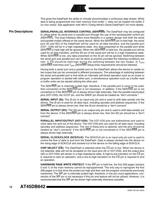
This gives the <strong>DataFlash</strong> the ability to virtually accommodate a continuous data stream. Whiledata is being programmed into main memory from buffer 1, data can be loaded into buffer 2(or vice versa). See application note AN-4 (“Using Atmel’s Serial <strong>DataFlash</strong>”) for more details.Pin DescriptionsSERIAL/PARALLEL INTERFACE CONTROL (SER/PAR): The <strong>DataFlash</strong> may be configuredto utilize either its serial port or parallel port through the use of the serial/parallel control pin(SER/PAR). The <strong>Dual</strong> Interface offers more flexibility in a system design with both the serialand parallel modes offered on the same device. When the SER/PAR pin is held high, the serialport (SI and SO) of the <strong>DataFlash</strong> will be used for all data transfers, and the parallel port(I/O7 - I/O0) will be in a high impedance state. Any data presented on the parallel port whileSER/PAR is held high will be ignored. When the SER/PAR is held low, the parallel port will beused for all data transfers, and the SO pin of the serial port will be in a high impedance state.While SER/PAR is low, any data presented on the SI pin will be ignored. Switching betweenthe serial port and parallel port can be done at anytime provided the following conditions aremet: 1) CS should be held high during the switching between the two modes. 2) T SPH(SER/PAR hold time) and T SPS (SER/PAR Setup time) requirements should be followed.Having both a serial port and a parallel port on the <strong>DataFlash</strong> allows the device to reside ontwo buses that can be connected to different processors. The advantage of switching betweenthe serial and parallel port is that while an internally self-timed operation such as an erase orprogram operation is started with either port, a simultaneous operation such as a buffer reador buffer write can be started utilizing the other port.The SER/PAR pin is internally pulled high; therefore, if the parallel port is never to be used,then connection of the SER/PAR pin is not necessary. In addition, if the SER/PAR pin is notconnected or if the SER/PAR pin is always driven high externally, then the parallel input/outputpins (I/O7-I/O0), the VCCP pin, and the GNDP pin should be treated as “don’t connects.”SERIAL INPUT (SI): The SI pin is an input-only pin and is used to shift data serially into thedevice. The SI pin is used for all data input, including opcodes and address sequences. If theSER/PAR pin is always driven low, then the SI pin should be a “don’t connect”.SERIAL OUTPUT (SO): The SO pin is an output-only pin and is used to shift data serially outfrom the device. If the SER/PAR pin is always driven low, then the SO pin should be a “don’tconnect”.PARALLEL INPUT/OUTPUT (I/O7-I/O0): The I/O7-I/O0 pins are bidirectional and used toclock data into and out of the device. The I/O7-I/O0 pins are used for all data input, includingopcodes and address sequences. The use of these pins is optional, and the pins should betreated as “don’t connects” if the SER/PAR pin is not connected or if the SER/PAR pin isalways driven high externally.SERIAL CLOCK/CLOCK (SCK/CLK): The SCK/CLK pin is an input-only pin and is used tocontrol the flow of data to and from the <strong>DataFlash</strong>. Data is always clocked into the device onthe rising edge of SCK/CLK and clocked out of the device on the falling edge of SCK/CLK.CHIP SELECT (CS): The <strong>DataFlash</strong> is selected when the CS pin is low. When the device isnot selected, data will not be accepted on the input pins (SI or I/O7-I/O0), and the output pins(SO or I/O7-I/O0) will remain in a high impedance state. A high-to-low transition on the CS pinis required to start an operation, and a low-to-high transition on the CS pinisrequiredtoendan operation.HARDWARE PAGE WRITE PROTECT: If the WP pin is held low, the first 256 pages (sectors0 and 1) of the main memory cannot be reprogrammed. The only way to reprogram the first256 pages is to first drive the protect pin high and then use the program commands previouslymentioned. The WP pin is internally pulled high; therefore, in low pin count applications, connectionof the WP pin is not necessary if this pin and feature will not be utilized. However, it isrecommended that the WP pin be driven high externally whenever possible.10 AT45DB<strong>64</strong>21638F–DFLSH–09/02


