64-megabit 2.7-volt Only Dual-interface DataFlash AT45DB642
64-megabit 2.7-volt Only Dual-interface DataFlash AT45DB642
64-megabit 2.7-volt Only Dual-interface DataFlash AT45DB642
- No tags were found...

You also want an ePaper? Increase the reach of your titles
YUMPU automatically turns print PDFs into web optimized ePapers that Google loves.
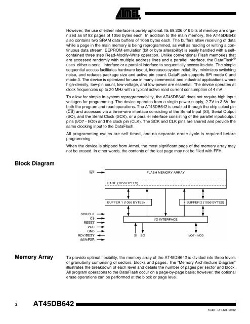
However, the use of either <strong>interface</strong> is purely optional. Its 69,206,016 bits of memory are organizedas 8192 pages of 1056 bytes each. In addition to the main memory, the AT45DB<strong>64</strong>2also contains two SRAM data buffers of 1056 bytes each. The buffers allow receiving of datawhile a page in the main memory is being reprogrammed, as well as reading or writing a continuousdata stream. EEPROM emulation (bit or byte alterability) is easily handled with a selfcontainedthree step Read-Modify-Write operation. Unlike conventional Flash memories thatare accessed randomly with multiple address lines and a parallel <strong>interface</strong>, the <strong>DataFlash</strong> ®uses either a serial <strong>interface</strong> or a parallel <strong>interface</strong> to sequentially access its data. The simplesequential access facilitates hardware layout, increases system reliability, minimizes switchingnoise, and reduces package size and active pin count. <strong>DataFlash</strong> supports SPI mode 0 andmode 3. The device is optimized for use in many commercial and industrial applications wherehigh-density, low-pin count, low-<strong>volt</strong>age, and low-power are essential. The device operates atclock frequencies up to 20 MHz with a typical active read current consumption of 4 mA.To allow for simple in-system reprogrammability, the AT45DB<strong>64</strong>2 does not require high input<strong>volt</strong>ages for programming. The device operates from a single power supply, <strong>2.7</strong>V to 3.6V, forboth the program and read operations. The AT45DB<strong>64</strong>2 is enabled through the chip select pin(CS) and accessed via a three-wire <strong>interface</strong> consisting of the Serial Input (SI), Serial Output(SO), and the Serial Clock (SCK), or a parallel <strong>interface</strong> consisting of the parallel input/outputpins (I/O7 - I/O0) and the clock pin (CLK). The SCK and CLK pins are shared and provide thesame clocking input to the <strong>DataFlash</strong>.All programming cycles are self-timed, and no separate erase cycle is required beforeprogramming.When the device is shipped from Atmel, the most significant page of the memory array maynot be erased. In other words, the contents of the last page may not be filled with FFH.Block DiagramWPFLASH MEMORY ARRAYPAGE (1056 BYTES)BUFFER 1 (1056 BYTES)BUFFER 2 (1056 BYTES)SCK/CLKCSRESETVCCGNDRDY/BUSYSER/PARSISOI/O INTERFACEI/O7 - I/O0Memory ArrayTo provide optimal flexibility, the memory array of the AT45DB<strong>64</strong>2 is divided into three levelsof granularity comprising of sectors, blocks and pages. The “Memory Architecture Diagram”illustrates the breakdown of each level and details the number of pages per sector and block.All program operations to the <strong>DataFlash</strong> occur on a page-by-page basis; however, the optionalerase operations can be performed at the block or page level.2 AT45DB<strong>64</strong>21638F–DFLSH–09/02