HT1608L 2Ã20 Channel LCD Driver
HT1608L 2Ã20 Channel LCD Driver
HT1608L 2Ã20 Channel LCD Driver

You also want an ePaper? Increase the reach of your titles
YUMPU automatically turns print PDFs into web optimized ePapers that Google loves.
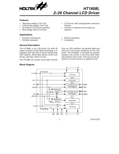
<strong>HT1608L</strong>2×20 <strong>Channel</strong> <strong>LCD</strong> <strong>Driver</strong>Features• Operating voltage: 2.7V~5.2V• <strong>LCD</strong> driving voltage: 3.0V~5.0V• 40 internal <strong>LCD</strong> drivers available• Bias voltage: static to 1/5 biasApplications• Electronic dictionaries• Portable computersGeneral DescriptionThe <strong>HT1608L</strong> is an <strong>LCD</strong> driver LSI with 40output channels using CMOS technology. It isequipped with two sets of 20-bit bidirectionalshift registers, 20-bit data latches, 20-bit <strong>LCD</strong>drivers, and logic control circuits.The HT1608 can convert serial data received• <strong>LCD</strong> driver with serial/parallel conversionfunction• Common or segment driver output byselection• Remote controllers• Calculatorsfrom an <strong>LCD</strong> controller into parallel data andsend out <strong>LCD</strong> driving waveforms to the <strong>LCD</strong>panel. The <strong>HT1608L</strong> is designed for generalpurpose <strong>LCD</strong> drivers. It can drive both staticand dynamic drive <strong>LCD</strong>s. The chip can be appliedto a common driver or a segment driver.Block Diagram1 27th Aug ’98
<strong>HT1608L</strong>Pin Assignment2 27th Aug ’98
<strong>HT1608L</strong>Pad AssignmentChip size: 101 × 115 (mil) 2* The IC substrate should be connected to VDD in the PCB layout artwork.3 27th Aug ’98
<strong>HT1608L</strong>Pad CoordinatesUnit: milPad No. X Y Pad No. X Y1 –44.54 51.94 31 44.12 –51.382 –44.54 45.86 32 44.12 –42.973 –44.54 39.78 33 44.12 –36.934 –44.54 33.70 34 42.33 –29.625 –44.54 27.63 35 44.12 –22.316 –44.54 21.55 36 44.12 –16.287 –44.54 15.47 37 44.12 –10.678 –44.54 9.39 38 44.12 –4.639 –44.54 3.32 39 44.12 0.9810 –44.54 –2.76 40 44.12 7.0111 –44.54 –8.84 41 44.12 12.6212 –44.54 –14.92 42 44.12 18.6613 –44.54 –21.00 43 44.12 24.3114 –44.54 –27.07 44 44.12 29.8315 –44.54 –33.15 45 44.12 35.3616 –44.54 –39.23 46 44.12 40.8817 –44.54 –45.31 47 44.12 46.4118 –44.54 –51.38 48 44.12 51.9419 –36.55 –51.38 49 31.28 51.9420 –29.92 –51.38 50 24.74 51.9421 –23.29 –51.38 51 18.19 51.9422 –16.66 –51.38 52 11.65 51.9423 –10.03 –51.38 53 5.10 51.9424 –3.40 –51.38 54 –1.45 51.9425 3.23 –51.38 55 –7.99 51.9426 9.86 –51.38 56 –14.53 51.9427 16.49 –51.38 57 –21.08 51.9428 23.12 –51.38 58 –27.63 51.9429 29.75 –51.38 59 –34.17 51.9430 36.38 –51.38Pad DescriptionPad No. Pad Name I/O Description1~9 Y28~Y20 O <strong>LCD</strong> driver outputs for channel 210~23 Y19~Y6 O <strong>LCD</strong> driver outputs for channel 124 VDD — Power supply ( positive )25~30 Y5~Y0 O <strong>LCD</strong> driver outputs for channel 131 VEE I <strong>LCD</strong> power supply32 CLK1 ILatch signal for channel 1 on the falling edgeCLK1 is used for channel 2 when MODE is set to V SS (Note 1 )4 27th Aug ’98
<strong>HT1608L</strong>Pad No. Pad Name I/O Description33 CLK2 IShift signal for channel 1 on the falling edge and used for channel 2when MODE is set to V SS (Note 1)34 VSS — Power supply (ground)35 DL1 I/O Data input/output of channel 1 shift register36 DR1 I/O Data input/output of channel 1 shift register37 DL2 I/O Data input/output of channel 2 shift register38 DR2 I/O Data input/output of channel 2 shift register39 ALT I Alternate signal input for <strong>LCD</strong> driving waveform40 SHF1 I Shift direction selection of channel 1 shift register (Note 2)41 SHF2 I Shift direction selection of channel 2 shift register (Note 2)42 MODE I Mode select signal of channel 2 (Note 3)43, 44 V1, V2 I <strong>LCD</strong> bias supply voltage for channels 1 and 245, 46 V3, V4 I <strong>LCD</strong> bias supply voltage for channel 147, 48 V5, V6 I <strong>LCD</strong> bias supply voltage for channel 249~59 Y39~Y29 O <strong>LCD</strong> driver outputs for channel 2Note 1: Data is processed on the clock falling or rising edge as shown in the following table.MODE= L (V SS)MODE= H (V DD)5 27th Aug ’98
<strong>HT1608L</strong>Note 2 : Shift direction of channel 1 and 2Shift Direction of <strong>Channel</strong> 1 (<strong>Channel</strong> 2)SHF1 (SHF2) DL1 (DL2) DR1 (DR2)H OUT INL IN OUTNote 3 :The output levels of channel 1 and 2 are decided by the combination of MODE, ALTand latched data. Refer to the following table:MODE Latched Data ALTH(V DD)L(V SS)HLHL<strong>Channel</strong> 1(Y0~Y19)<strong>Channel</strong> 2(Y20~Y39)H V1 V2L V2 V1H V3 V6L V4 V5H V1 V1L V2 V2H V3 V5L V4 V66 27th Aug ’98
<strong>HT1608L</strong>Absolute Maximum Ratings*Supply Voltage ..............................–0.3V to 5.5V Storage Temperature................. –50°C to 125°CInput Voltage................. V SS–0.3V to V DD+0.3V Operating Temperature............... –20°C to 70°C*Note: These are stress ratings only. Stresses exceeding the range specified under “Absolute MaximumRatings” may cause substantial damage to the device. Functional operation of thisdevice at other conditions beyond those listed in the specification is not implied and prolongedexposure to extreme conditions may affect device reliability.D.C. CharacteristicsTa=25°CSymbol ParameterTest ConditionsV DDConditionsMin. Typ. Max. UnitV DD Operating Voltage — — 2.7 — 5.2 VI DD Operating Current 5V No load — 100 300 µAI STB Standby Current 5V — — 1 5 µAf CLK2 Data Shift Frequency 5V — — — 400 kHztw CLK Clock Pulse Width 5V — 800 — — nsV IL “L” Input Voltage 5V — — — 1 VV IH “H” Input Voltage 5V — 4 — — VV OL “L” Output Voltage 5V I OL=+0.4mA — — 0.4 VV OH “H” Output Voltage 5V I OH=–0.4mA 4.6 — — VV <strong>LCD</strong> <strong>LCD</strong> Driving Voltage — V DD–V EE 3 — 5.0 V7 27th Aug ’98
<strong>HT1608L</strong>Functional DescriptionBoth channel 1 and 2 used as segment drivers (MODE=L)When both channel 1 and 2 of the <strong>HT1608L</strong> are used as segment drivers, they will shift data on thefalling edge of CLK2 and shift latch data on the falling edge of CLK1. V3 and V5 or V4 and V6 areshortened in the application circuit as shown in the following figure.Both channel 1 and 2 used as common drivers (MODE=L)When both channel 1 and 2 of the <strong>HT1608L</strong> are used as common drivers, the MODE is set low andthe signals (CLK1, CLK2, FRAME) from the controller are connected as shown in the followingfigure.8 27th Aug ’98
<strong>HT1608L</strong><strong>Channel</strong> 1 used as a segment driver and channel 2 as a common driver (MODE=H)When channel 2 is used as a common driver, MODE is connected to VDD. <strong>Channel</strong> 2 will shift dataon the rising edge of CLK1 and shift latch data on the rising edge of CLK2.Static driverWhen the <strong>HT1608L</strong> is used as a static driver, data is transferred on the falling edge of CLK2 andlatched on the falling edge of CLK1. The frequency of CLK1 becomes the frame frequency of the <strong>LCD</strong>driver. The frequency of ALT has to be twice the frequency of CLK1. ALT has to be synchronized onthe falling edge of CLK1.The power supply for the <strong>LCD</strong> driver is used by shortening V1, V4 and V6 or V2, V3 and V5. One ofthe <strong>LCD</strong> output terminals can be used as a common output. The application circuit connections areshown below:9 27th Aug ’98
<strong>HT1608L</strong>Timing DiagramsSegment data waveform (1/8 duty)10 27th Aug ’98
<strong>HT1608L</strong>Common data waveform (a typical waveform of channel 2 as a COMMON driver, 1/8 duty)11 27th Aug ’98
<strong>HT1608L</strong>Application Circuits12 27th Aug ’98
<strong>HT1608L</strong>Holtek Semiconductor Inc. (Headquarters)No.3, Creation Rd. II, Science-based Industrial Park, Hsinchu, Taiwan, R.O.C.Tel: 886-3-563-1999Fax: 886-3-563-1189Holtek Semiconductor Inc. (Taipei Office)11F, No.576, Sec.7 Chung Hsiao E. Rd., Taipei, Taiwan, R.O.C.Tel: 886-2-2782-9635Fax: 886-2-2782-9636Fax: 886-2-2782-7128 (International sales hotline)Holtek Semiconductor (Hong Kong) Ltd.RM.711, Tower 2, Cheung Sha Wan Plaza, 833 Cheung Sha Wan Rd., Kowloon, Hong KongTel: 852-2-745-8288Fax: 852-2-742-8657Holtek Semiconductor (Shanghai) Ltd.7th Floor, Building 2, No.889, Yi Shan Rd., Shanghai, ChinaTel: 021-6485-5560Fax: 021-6485-0313Holmate Technology Corp.48531 Warm Springs Boulevard, Suite 413, Fremont, CA 94539Tel: 510-252-9880Fax: 510-252-9885Copyright 1998 by HOLTEK SEMICONDUCTOR INC.The information appearing in this Data Sheet is believed to be accurate at the time of publication. However, Holtekassumes no responsibility arising from the use of the specifications described. The applications mentioned herein areused solely for the purpose of illustration and Holtek makes no warranty or representation that such applicationswill be suitable without further modification, nor recommends the use of its products for application that may presenta risk to human life due to malfunction or otherwise. Holtek reserves the right to alter its products without priornotification. For the most up-to-date information, please visit our web site at http://www.holtek.com.tw.13 27th Aug '98