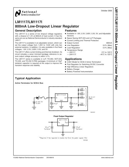
LM1117/LM1117I 800mA Low-Dropout Linear Regulator
LM1117/LM1117I 800mA Low-Dropout Linear Regulator
LM1117/LM1117I 800mA Low-Dropout Linear Regulator
You also want an ePaper? Increase the reach of your titles
YUMPU automatically turns print PDFs into web optimized ePapers that Google loves.
Block Diagram<strong>LM1117</strong>/<strong>LM1117</strong>I10091901Connection DiagramsTO-263SOT-22310091944Top ViewTop View10091904TO-22010091945Side ViewLLPTop View10091902TO-252Top View10091938When using the LLP packagePins 2, 3&4must be connected together andPins 5, 6&7must be connected togetherTop View100919463www.national.com
<strong>LM1117</strong>/<strong>LM1117</strong>IAbsolute Maximum Ratings (Note 1)If Military/Aerospace specified devices are required,please contact the National Semiconductor Sales Office/Distributors for availability and specifications.Maximum Input Voltage (V IN to GND)Power Dissipation (Note 2)Junction Temperature (T J )(Note 2)Storage Temperature RangeLead TemperatureTO-220 (T) Package20VInternally Limited150˚C-65˚C to 150˚C260˚C, 10 secSOT-223 (IMP) Package260˚C, 4 secESD Tolerance (Note 3)2000VOperating Ratings (Note 1)Input Voltage (V IN to GND)15VJunction Temperature Range (T J )(Note 2)<strong>LM1117</strong>0˚C to 125˚C<strong>LM1117</strong>I−40˚C to 125˚C<strong>LM1117</strong> Electrical CharacteristicsTypicals and limits appearing in normal type apply for T J = 25˚C. Limits appearing in Boldface type apply over the entire junctiontemperature range for operation, 0˚C to 125˚C.Symbol Parameter ConditionsV REF Reference Voltage <strong>LM1117</strong>-ADJI OUT = 10mA, V IN -V OUT = 2V, T J = 25˚C10mA ≤ I OUT ≤ <strong>800mA</strong>, 1.4V ≤ V IN -V OUT≤ 10VV OUT Output Voltage <strong>LM1117</strong>-1.8I OUT = 10mA, V IN = 3.8V, T J = 25˚C0 ≤ I OUT ≤ <strong>800mA</strong>, 3.2V ≤ V IN ≤ 10V<strong>LM1117</strong>-2.5I OUT = 10mA, V IN = 4.5V, T J = 25˚C0 ≤ I OUT ≤ <strong>800mA</strong>, 3.9V ≤ V IN ≤ 10V<strong>LM1117</strong>-2.85I OUT = 10mA, V IN = 4.85V, T J = 25˚C0 ≤ I OUT ≤ <strong>800mA</strong>, 4.25V ≤ V IN ≤ 10V0 ≤ I OUT ≤ 500mA, V IN = 4.10V<strong>LM1117</strong>-3.3I OUT = 10mA, V IN =5VT J = 25˚C0 ≤ I OUT ≤ <strong>800mA</strong>, 4.75V≤ V IN ≤ 10V<strong>LM1117</strong>-5.0I OUT = 10mA, V IN = 7V, T J = 25˚C0 ≤ I OUT ≤ <strong>800mA</strong>, 6.5V ≤ V IN ≤ 12V∆V OUTLine Regulation(Note 6)Min(Note 5)1.2381.2251.7821.7462.4752.4502.8202.7902.7903.2673.2354.9504.900Typ(Note 4)1.2501.2501.8001.8002.5002.5002.8502.8502.8503.3003.3005.0005.000Max(Note 5)1.2621.2701.8181.8542.5252.5502.8802.9102.9103.3333.3655.0505.100Units<strong>LM1117</strong>-ADJI OUT = 10mA, 1.5V ≤ V IN -V OUT ≤ 13.75V 0.035 0.2 %<strong>LM1117</strong>-1.81 6 mVI OUT = 0mA, 3.2V ≤ V IN ≤ 10V<strong>LM1117</strong>-2.51 6 mVI OUT = 0mA, 3.9V ≤ V IN ≤ 10V<strong>LM1117</strong>-2.85I OUT = 0mA, 4.25V ≤ V IN ≤ 10V 1 6 mV<strong>LM1117</strong>-3.3I OUT = 0mA, 4.75V ≤ V IN ≤ 15V 1 6 mV<strong>LM1117</strong>-5.0I OUT = 0mA, 6.5V ≤ V IN ≤ 15V 1 10 mVVVVVVVVVVVVVVwww.national.com 4
<strong>LM1117</strong> Electrical Characteristics (Continued)Typicals and limits appearing in normal type apply for T J = 25˚C. Limits appearing in Boldface type apply over the entire junctiontemperature range for operation, 0˚C to 125˚C.Symbol Parameter Conditions∆V OUTLoad Regulation(Note 6)Min(Note 5)Typ(Note 4)Max(Note 5)Units<strong>LM1117</strong>-ADJV IN -V OUT = 3V, 10 ≤ I OUT ≤ <strong>800mA</strong> 0.2 0.4 %<strong>LM1117</strong>-1.81 10 mVV IN = 3.2V, 0 ≤ I OUT ≤ <strong>800mA</strong><strong>LM1117</strong>-2.51 10 mVV IN = 3.9V, 0 ≤ I OUT ≤ <strong>800mA</strong><strong>LM1117</strong>-2.85V IN = 4.25V, 0 ≤ I OUT ≤ <strong>800mA</strong> 1 10 mV<strong>LM1117</strong>-3.3V IN = 4.75V, 0 ≤ I OUT ≤ <strong>800mA</strong> 1 10 mV<strong>LM1117</strong>-5.0V IN = 6.5V, 0 ≤ I OUT ≤ <strong>800mA</strong> 1 15 mVV IN -V OUT <strong>Dropout</strong> Voltage I OUT = 100mA 1.10 1.20 V(Note 7)I OUT = 500mA 1.15 1.25 VI OUT = <strong>800mA</strong> 1.20 1.30 VI LIMIT Current Limit V IN -V OUT = 5V, T J = 25˚C 800 1200 1500 mAMinimum LoadCurrent (Note 8)Quiescent Current<strong>LM1117</strong>-ADJV IN = 15V 1.7 5 mA<strong>LM1117</strong>-1.85 10 mAV IN ≤ 15V<strong>LM1117</strong>-2.55 10 mAV IN ≤ 15V<strong>LM1117</strong>-2.85V IN ≤ 10V 5 10 mA<strong>LM1117</strong>-3.3V IN ≤ 15V 5 10 mA<strong>LM1117</strong>-5.0V IN ≤ 15V 5 10 mA60Thermal Regulation T A = 25˚C, 30ms Pulse 0.01 0.1 %/WRipple Regulation f RIPPLE =1 20Hz, V IN -V OUT =3VV RIPPLE75 dB=1V PPAdjust Pin Current 60 120 µAAdjust Pin CurrentChange10 ≤ I OUT ≤ <strong>800mA</strong>,1.4V ≤ V IN -V OUT ≤ 10V 0.2 5 µATemperature Stability 0.5 %Long Term Stability T A = 125˚C, 1000Hrs 0.3 %RMS Output Noise (% of V OUT ), 10Hz ≤ f ≤10kHz 0.003 %Thermal Resistance 3-Lead SOT-223 15.0 ˚C/WJunction-to-Case 3-Lead TO-220 3.0 ˚C/W3-Lead TO-252 10 ˚C/WThermal Resistance 3-Lead SOT-223 (No heat sink) 136 ˚C/WJunction-to-Ambient 3-Lead TO-220 (No heat sink) 79 ˚C/W(No air flow)3-Lead TO-252 (Note 9) (No heat sink) 92 ˚C/W3-Lead TO-263 55 ˚C/W8-Lead LLP(Note 10) 40 ˚C/W<strong>LM1117</strong>/<strong>LM1117</strong>I5www.national.com
<strong>LM1117</strong>/<strong>LM1117</strong>I<strong>LM1117</strong>I Electrical CharacteristicsTypicals and limits appearing in normal type apply for T J = 25˚C. Limits appearing in Boldface type apply over the entire junctiontemperature range for operation, −40˚C to 125˚C.Symbol Parameter ConditionsV REF Reference Voltage <strong>LM1117</strong>I-ADJI OUT = 10mA, V IN -V OUT = 2V, T J = 25˚C10mA ≤ I OUT ≤ <strong>800mA</strong>, 1.4V ≤ V IN -V OUT≤ 10VV OUT Output Voltage <strong>LM1117</strong>I-3.3I OUT = 10mA, V IN = 5V, T J = 25˚C0 ≤ I OUT ≤ <strong>800mA</strong>, 4.75V ≤ V IN ≤ 10V<strong>LM1117</strong>I-5.0I OUT = 10mA, V IN = 7V, T J = 25˚C0 ≤ I OUT ≤ <strong>800mA</strong>, 6.5V ≤ V IN ≤ 12V∆V OUT∆V OUTLine Regulation(Note 6)Load Regulation(Note 6)Min(Note 5)1.2381.2003.2673.1684.9504.800Typ(Note 4)1.2501.2503.3003.3005.0005.000Max(Note 5)1.2621.2903.3333.4325.0505.200Units<strong>LM1117</strong>I-ADJI OUT = 10mA, 1.5V ≤ V IN -V OUT ≤ 13.75V 0.035 0.3 %<strong>LM1117</strong>I-3.3I OUT = 0mA, 4.75V ≤ V IN ≤ 15V 1 10 mV<strong>LM1117</strong>I-5.0I OUT = 0mA, 6.5V ≤ V IN ≤ 15V 1 15 mV<strong>LM1117</strong>I-ADJV IN -V OUT = 3V, 10 ≤ I OUT ≤ <strong>800mA</strong> 0.2 0.5 %<strong>LM1117</strong>I-3.3V IN = 4.75V, 0 ≤ I OUT ≤ <strong>800mA</strong> 1 15 mV<strong>LM1117</strong>I-5.0V IN = 6.5V, 0 ≤ I OUT ≤ <strong>800mA</strong> 1 20 mVV IN -V OUT <strong>Dropout</strong> Voltage I OUT = 100mA 1.10 1.30 V(Note 7)I OUT = 500mA 1.15 1.35 VI OUT = <strong>800mA</strong> 1.20 1.40 VI LIMIT Current Limit V IN -V OUT = 5V, T J = 25˚C 800 1200 1500 mAMinimum LoadCurrent (Note 8)Quiescent Current<strong>LM1117</strong>I-ADJV IN = 15V 1.7 5 mA<strong>LM1117</strong>I-3.3V IN ≤ 15V 5 15 mA<strong>LM1117</strong>I-5.0V IN ≤ 15V 5 15 mA60Thermal Regulation T A = 25˚C, 30ms Pulse 0.01 0.1 %/WRipple Regulation f RIPPLE =1 20Hz, V IN -V OUT =3VV RIPPLE75 dB=1V PPAdjust Pin Current 60 120 µAAdjust Pin CurrentChange10 ≤ I OUT ≤ <strong>800mA</strong>,1.4V ≤ V IN -V OUT ≤ 10V 0.2 10 µATemperature Stability 0.5 %Long Term Stability T A = 125˚C, 1000Hrs 0.3 %RMS Output Noise (% of V OUT ), 10Hz ≤ f ≤10kHz 0.003 %Thermal Resistance 3-Lead SOT-223 15.0 ˚C/WJunction-to-Case 3-Lead TO-252 10 ˚C/WThermal Resistance 3-Lead SOT-223 (No heat sink) 136 ˚C/WJunction-to-Ambient 3-Lead TO-252 (No heat sink)(Note 9) 92 ˚C/WNo air flow)8-Lead LLP(Note 10) 40 ˚C/WVVVVVVNote 1: Absolute Maximum Ratings indicate limits beyond which damage to the device may occur. Operating Ratings indicate conditions for which the device isintended to be functional, but specific performance is not guaranteed. For guaranteed specifications and the test conditions, see the Electrical Characteristics.www.national.com 6
Note 2: The maximum power dissipation is a function of T J(max) , θ JA , and T A . The maximum allowable power dissipation at any ambient temperature isP D =(T J(max) –T A )/θ JA . All numbers apply for packages soldered directly into a PC board.Note 3: For testing purposes, ESD was applied using human body model, 1.5kΩ in series with 100pF.Note 4: Typical Values represent the most likely parametric norm.Note 5: All limits are guaranteed by testing or statistical analysis.Note 6: Load and line regulation are measured at constant junction room temperature.Note 7: The dropout voltage is the input/output differential at which the circuit ceases to regulate against further reduction in input voltage. It is measured when theoutput voltage has dropped 100mV from the nominal value obtained at V IN =V OUT +1.5V.Note 8: The minimum output current required to maintain regulation.Note 9: Minimum pad size of 0.038in 2Note 10: Thermal Performance for the LLP was obtained using JESD51-7 board with six vias and an ambient temperature of 22˚C. For information about improvedthermal performance and power dissipation for the LLP, refer to Application Note AN-1187.<strong>LM1117</strong>/<strong>LM1117</strong>ITypical Performance Characteristics<strong>Dropout</strong> Voltage (V IN -V OUT )Short-Circuit Current10091922 10091923Load Regulation<strong>LM1117</strong>-ADJ Ripple Rejection10091943100919067www.national.com
<strong>LM1117</strong>/<strong>LM1117</strong>ITypical Performance Characteristics (Continued)<strong>LM1117</strong>-ADJ Ripple Rejection vs. CurrentTemperature Stability10091907 10091925Adjust Pin Current<strong>LM1117</strong>-2.85 Load Transient Response10091926 10091908<strong>LM1117</strong>-5.0 Load Transient Response<strong>LM1117</strong>-2.85 Line Transient Response10091909 10091910www.national.com 8
<strong>LM1117</strong>/<strong>LM1117</strong>IApplication Note (Continued)With an extremely large output capacitor (≥1000 µF), andwith input instantaneously shorted to ground, the regulatorcould be damaged.In this case, an external diode is recommended between theoutput and input pins to protect the regulator, as shown inFigure 4.10091918FIGURE 2. Typical Application using Fixed Output<strong>Regulator</strong>When the adjustable regulator is used (Figure 3), the bestperformance is obtained with the positive side of the resistorR1 tied directly to the output terminal of the regulator ratherthan near the load. This eliminates line drops from appearingeffectively in series with the reference and degrading regulation.For example, a 5V regulator with 0.05Ω resistancebetween the regulator and load will have a load regulationdue to line resistance of 0.05Ω xI L . If R1 (=125Ω) is connectednear the load, the effective line resistance will be0.05Ω (1+R2/R1) or in this case, it is 4 times worse. Inaddition, the ground side of the resistor R2 can be returnednear the ground of the load to provide remote ground sensingand improve load regulation.FIGURE 4. <strong>Regulator</strong> with Protection Diode100919155.0 Heatsink RequirementsWhen an integrated circuit operates with an appreciablecurrent, its junction temperature is elevated. It is important toquantify its thermal limits in order to achieve acceptableperformance and reliability. This limit is determined by summingthe individual parts consisting of a series of temperaturerises from the semiconductor junction to the operatingenvironment. A one-dimensional steady-state model of conductionheat transfer is demonstrated in Figure 5. The heatgenerated at the device junction flows through the die to thedie attach pad, through the lead frame to the surroundingcase material, to the printed circuit board, and eventually tothe ambient environment. Below is a list of variables thatmay affect the thermal resistance and in turn the need for aheatsink.10091919FIGURE 3. Best Load Regulation using AdjustableOutput <strong>Regulator</strong>4.0 Protection DiodesUnder normal operation, the <strong>LM1117</strong> regulators do not needany protection diode. With the adjustable device, the internalresistance between the adjust and output terminals limits thecurrent. No diode is needed to divert the current around theregulator even with capacitor on the adjust terminal. Theadjust pin can take a transient signal of ±25V with respect tothe output voltage without damaging the device.When a output capacitor is connected to a regulator and theinput is shorted to ground, the output capacitor will dischargeinto the output of the regulator. The discharge current dependson the value of the capacitor, the output voltage of theregulator, and rate of decrease of V IN . In the <strong>LM1117</strong> regulators,the internal diode between the output and input pinscan withstand microsecond surge currents of 10A to 20A.R θ JC (ComponentVariables)Leadframe Size & MaterialNo. of Conduction PinsDie SizeDie Attach MaterialMolding Compound Sizeand MaterialR θ CA (ApplicationVariables)Mounting Pad Size,Material, & LocationPlacement of MountingPadPCB Size & MaterialTraces Length & WidthAdjacent Heat SourcesVolume of AirAmbient TemperatueShape of Mounting Padwww.national.com 10
Application Note (Continued)<strong>LM1117</strong>/<strong>LM1117</strong>I1009193710091916FIGURE 5. Cross-sectional view of Integrated CircuitMounted on a printed circuit board. Note that the casetemperature is measured at the point where the leadscontact with the mounting pad surfaceThe <strong>LM1117</strong> regulators have internal thermal shutdown toprotect the device from over-heating. Under all possibleoperating conditions, the junction temperature of the <strong>LM1117</strong>must be within the range of 0˚C to 125˚C. A heatsink may berequired depending on the maximum power dissipation andmaximum ambient temperature of the application. To determineif a heatsink is needed, the power dissipated by theregulator, P D , must be calculated:I IN =I L +I GP D =(V IN -V OUT )I L +V IN I GFigure 6 shows the voltages and currents which are presentin the circuit.FIGURE 6. Power Dissipation DiagramThe next parameter which must be calculated is the maximumallowable temperature rise, T R (max):T R (max) = T J (max)-T A (max)where T J (max) is the maximum allowable junction temperature(125˚C), and T A (max) is the maximum ambient temperaturewhich will be encountered in the application.Using the calculated values for T R (max) and P D , the maximumallowable value for the junction-to-ambient thermalresistance (θ JA ) can be calculated:θ JA =T R (max)/P DIf the maximum allowable value for θ JA is found to be≥136˚C/W for SOT-223 package or ≥79˚C/W for TO-220package or ≥92˚C/W for TO-252 package, no heatsink isneeded since the package alone will dissipate enough heatto satisfy these requirements. If the calculated value for θ JAfalls below these limits, a heatsink is required.As a design aid, Table 1 shows the value of the θ JA ofSOT-223 and TO-252 for different heatsink area. The copperpatterns that we used to measure these θ JA s are shown atthe end of the Application Notes Section. Figure 7 and Figure8 reflects the same test results as what are in the Table 1Figure 9 and Figure 10 shows the maximum allowable powerdissipation vs. ambient temperature for the SOT-223 andTO-252 device. Figures Figure 11 and Figure 12 shows themaximum allowable power dissipation vs. copper area (in 2 )for the SOT-223 and TO-252 devices. Please see AN1028for power enhancement techniques to be used with SOT-223and TO-252 packages.*Application Note AN-1187 discusses improved thermal performanceand power dissipation for the LLP.TABLE 1. θ JA Different Heatsink AreaLayout Copper Area Thermal ResistanceTop Side (in 2 )* Bottom Side (in 2 ) (θ JA ,˚C/W) SOT-223 (θ JA ,˚C/W) TO-2521 0.0123 0 136 1032 0.066 0 123 873 0.3 0 84 604 0.53 0 75 545 0.76 0 69 526 1 0 66 477 0 0.2 115 848 0 0.4 98 709 0 0.6 89 6310 0 0.8 82 5711 0 1 79 5712 0.066 0.066 125 8911www.national.com
<strong>LM1117</strong>/<strong>LM1117</strong>IApplication Note (Continued)TABLE 1. θ JA Different Heatsink Area (Continued)Layout Copper Area Thermal Resistance13 0.175 0.175 93 7214 0.284 0.284 83 6115 0.392 0.392 75 5516 0.5 0.5 70 53*Tab of device attached to topside copperwww.national.com 12
Application Note (Continued)<strong>LM1117</strong>/<strong>LM1117</strong>I1009193610091913FIGURE 7. θ JA vs. 1oz Copper Area for SOT-223FIGURE 10. Maximum Allowable Power Dissipation vs.Ambient Temperature for TO-2521009193410091914FIGURE 8. θ JA vs. 2oz Copper Area for TO-252FIGURE 11. Maximum Allowable Power Dissipation vs.1oz Copper Area for SOT-2231009191210091935FIGURE 9. Maximum Allowable Power Dissipation vs.Ambient Temperature for SOT-223FIGURE 12. Maximum Allowable Power Dissipation vs.2oz Copper Area for TO-25213www.national.com
<strong>LM1117</strong>/<strong>LM1117</strong>IApplication Note (Continued)10091941FIGURE 13. Top View of the Thermal Test Pattern in Actual Scalewww.national.com 14
Application Note (Continued)<strong>LM1117</strong>/<strong>LM1117</strong>I10091942FIGURE 14. Bottom View of the Thermal Test Pattern in Actual Scale15www.national.com
<strong>LM1117</strong>/<strong>LM1117</strong>ITypical Application CircuitsAdjusting Output of Fixed <strong>Regulator</strong>s10091930100919275V Logic <strong>Regulator</strong> with Electronic Shutdown*<strong>Regulator</strong> with Reference10091931100919291.25V to 10V Adjustable <strong>Regulator</strong> with ImprovedRipple Rejectionwww.national.com 16
Typical Application Circuits (Continued)<strong>LM1117</strong>/<strong>LM1117</strong>IBattery Backed-Up Regulated Supply10091932<strong>Low</strong> <strong>Dropout</strong> Negative Supply1009193317www.national.com
<strong>LM1117</strong>/<strong>LM1117</strong>IPhysical Dimensions inches (millimeters)unless otherwise noted3-Lead SOT-223NS Package Number MP04Awww.national.com 18
Physical Dimensions inches (millimeters) unless otherwise noted (Continued)<strong>LM1117</strong>/<strong>LM1117</strong>I3-Lead TO-220NS Package Number T03B19www.national.com
<strong>LM1117</strong>/<strong>LM1117</strong>IPhysical Dimensions inches (millimeters) unless otherwise noted (Continued)3-Lead TO-263NS Package Number TS3Bwww.national.com 20
Physical Dimensions inches (millimeters) unless otherwise noted (Continued)<strong>LM1117</strong>/<strong>LM1117</strong>I3-Lead TO-252NS Package Number TD03B8-Lead LLPNS Package Number LDC08A21www.national.com
<strong>LM1117</strong>/<strong>LM1117</strong>I <strong>800mA</strong> <strong>Low</strong>-<strong>Dropout</strong> <strong>Linear</strong> <strong>Regulator</strong>NotesLIFE SUPPORT POLICYNATIONAL’S PRODUCTS ARE NOT AUTHORIZED FOR USE AS CRITICAL COMPONENTS IN LIFE SUPPORTDEVICES OR SYSTEMS WITHOUT THE EXPRESS WRITTEN APPROVAL OF THE PRESIDENT AND GENERALCOUNSEL OF NATIONAL SEMICONDUCTOR CORPORATION. As used herein:1. Life support devices or systems are devices orsystems which, (a) are intended for surgical implantinto the body, or (b) support or sustain life, andwhose failure to perform when properly used inaccordance with instructions for use provided in thelabeling, can be reasonably expected to result in asignificant injury to the user.2. A critical component is any component of a lifesupport device or system whose failure to performcan be reasonably expected to cause the failure ofthe life support device or system, or to affect itssafety or effectiveness.National SemiconductorCorporationAmericasEmail: support@nsc.comwww.national.comNational SemiconductorEuropeFax: +49 (0) 180-530 85 86Email: europe.support@nsc.comDeutsch Tel: +49 (0) 69 9508 6208English Tel: +44 (0) 870 24 0 2171Français Tel: +33 (0) 1 41 91 8790National SemiconductorAsia Pacific CustomerResponse GroupTel: 65-2544466Fax: 65-2504466Email: ap.support@nsc.comNational SemiconductorJapan Ltd.Tel: 81-3-5639-7560Fax: 81-3-5639-7507National does not assume any responsibility for use of any circuitry described, no circuit patent licenses are implied and National reserves the right at any time without notice to change said circuitry and specifications.


