Dual 10-Ohm SPDT Analog Switch (Rev. D)
Dual 10-Ohm SPDT Analog Switch (Rev. D)
Dual 10-Ohm SPDT Analog Switch (Rev. D)

Create successful ePaper yourself
Turn your PDF publications into a flip-book with our unique Google optimized e-Paper software.
TS5A23157SCDS165D–MAY 2004–REVISED MAY 2008 ................................................................................................................................................................ www.ti.comSUMMARY OF CHARACTERISTICSConfiguration2:1 Multiplexer/Demultiplexer(2 × <strong>SPDT</strong>)Number of channels 2ON-state resistance (r on ) <strong>10</strong> ΩON-state resistance matchbetween channels (Δr on )0.15 ΩON-state resistance flatness(r on(flat) )4 ΩTurn-on/turn-off time (t ON /t OFF ) 5.7 ns/3.8 nsBreak-before-make time (t BBM ) 0.5 nsCharge injection (Q C )7 pCBandwidth (BW)220 MHzOFF isolation (OSIO)–65 dB at <strong>10</strong> MHzCrosstalk 9XTALK)–66 dB at <strong>10</strong> MHzTotal harmo nic distortion (THD) 0.01%Leakage current(I COM(OFF) /I NC(OFF) )±1 µAPackage options<strong>10</strong>-pin DGS and RSEABSOLUTE MAXIMUM RATINGS (1)over operating free-air temperature range (unless otherwise noted)MIN MAX UNITV + Supply voltage range (2) –0.5 6.5 VV NCV NO <strong>Analog</strong> voltage range (2)(3)(4) –0.5 V + + 0.5 VV COMI I/OK <strong>Analog</strong> port diode currentV NC , V NO , V COM < 0 or V NC , V NO ,V COM > V +±50 mAI NCI NO On-state switch current V NC , V NO , V COM = 0 to V + ±50 mAI COMV IN Digital input voltage range (2)(3) –0.5 6.5 VI IK Digital input clamp current V IN < 0 –50 mAContinuous current through V + or GND ±<strong>10</strong>0 mADGS package 56.5θ JA Package thermal impedance (5) °C/WRSE package 243T stg Storage temperature range –65 150 °C(1) Stresses beyond those listed under "absolute maximum ratings" may cause permanent damage to the device. These are stress ratingsonly, and functional operation of the device at these or any other conditions beyond those indicated under "recommended operatingconditions" is not implied. Exposure to absolute-maximum-rated conditions for extended periods may affect device reliability.(2) All voltages are with respect to ground, unless otherwise specified.(3) The input and output voltage ratings may be exceeded if the input and output clamp-current ratings are observed.(4) This value is limited to 5.5 V maximum.(5) The package thermal impedance is calculated in accordance with JESD 51-7.2 Submit Documentation Feedback Copyright © 2004–2008, Texas Instruments IncorporatedProduct Folder Link(s): TS5A23157
TS5A23157www.ti.com ................................................................................................................................................................ SCDS165D–MAY 2004–REVISED MAY 2008ELECTRICAL CHARACTERISTICS FOR 5-V SUPPLYV + = 4.5 V to 5.5 V, T A = –40°C to 85°C (unless otherwise noted)PARAMETER SYMBOL TEST CONDITIONS T A V + MIN TYP (1) MAX UNIT<strong>Analog</strong> <strong>Switch</strong>V COM ,<strong>Analog</strong> signal range 0 V + VV NO , V NC0 ≤ V NO or V NC ≤ V + , <strong>Switch</strong> ON,ON-state resistance r on Full 4.5 V <strong>10</strong> ΩI COM = –30 mA, See Figure <strong>10</strong>ON-state resistanceV NO or V NC = 3.15 V, <strong>Switch</strong> ON,match between Δr on 25°C 4.5 V 0.15 ΩI COM = –30 mA, See Figure <strong>10</strong>channelsON-state resistance 0 ≤ V NO or V NC ≤ V + , <strong>Switch</strong> ON,r on(flat) 25°C 4.5 V 4 Ωflatness I COM = –30 mA, See Figure <strong>10</strong>NC, NO I NC(OFF) , V NC or V NO = 0 to V + , <strong>Switch</strong> OFF, 25°C –1 0.05 15.5 V µAOFF leakage current I NO(OFF) V COM = 0 to V + , See Figure 11 Full –1 1NC, NO I NC(ON) , V NC or V NO = 0 to V + , <strong>Switch</strong> ON, 25°C –0.1 0.15.5 V µAON leakage current I NO(ON) V COM = Open, See Figure 11 Full –1 1COM V NC or V NO = Open, <strong>Switch</strong> ON, 25°C –0.1 0.1I COM(ON) 5.5 V µAON leakage current V COM = 0 to V + , See Figure 11 Full –1 1Digital Inputs (IN12, IN2) (2) V +Input logic high VIH Full V× 0.7V +Input logic low VIL Full V× 0.325°C –1 0.05 1Input leakage current I IH , I IL V IN = 5.5 V or 0 5.5 V µAFull –1 1(1) T A = 25°C(2) All unused digital inputs of the device must be held at V+ or GND to ensure proper device operation. Refer to the TI application report,Implications of Slow or Floating CMOS Inputs, literature number SCBA004.Copyright © 2004–2008, Texas Instruments Incorporated Submit Documentation Feedback 3Product Folder Link(s): TS5A23157
TS5A23157SCDS165D–MAY 2004–REVISED MAY 2008 ................................................................................................................................................................ www.ti.comELECTRICAL CHARACTERISTICS FOR 5-V SUPPLY (continued)V + = 4.5 V to 5.5 V, T A = –40°C to 85°C (unless otherwise noted)PARAMETER SYMBOL TEST CONDITIONS T A V + MIN TYP (1) MAX UNITDynamicV NC = GND and V NO = V + R L = 500 Ω,4.5 V toTurn-on time t ON or C L = 50 pF, Full 1.7 5.7 ns5.5 VV NC = V + and V NO = GND, See Figure 13V NC = GND and V NO = V + R L = 500 Ω,4.5 V toTurn-off time t OFF or C L = 50 pF, Full 0.8 3.8 ns5.5 VV NC = V + and V NO = GND, See Figure 13Break-before-make V NC = V NO = V + /2, C L = 35 pF, 4.5 V tot BBM Full 0.5 nstime R L = 50 Ω, See Figure 14 5.5 VV NC = V NO = V + /2,Charge injection Q C See Figure 18 25°C 5 V 7 pCR L = 50 Ω,NC, NO C NC(OFF) , <strong>Switch</strong> OFF,V NC or V NO = V + or GND, 25°C 5 V 5.5 pFOFF capacitance C NO(OFF) See Figure 12NC, NO C NC(ON) , <strong>Switch</strong> ON,V NC or V NO = V + or GND, 25°C 5 V 17.5 pFON capacitance C NO(ON) See Figure 12COM<strong>Switch</strong> ON,C COM(ON) V COM = V + or GND, 25°C 5 V 17.5 pFON capacitance See Figure 12Digital inputcapacitanceC IN V IN = V + or GND, See Figure 12 25°C 5 V 2.8 pF<strong>Switch</strong> ON,Bandwidth BW R L = 50 Ω, 25°C 4.5 V 220 MHzSee Figure 15R L = 50 Ω,<strong>Switch</strong> OFF,OFF isolation O ISO 25°C 4.5 V –65 dBf = <strong>10</strong> MHz, See Figure 16R L = 50 Ω,<strong>Switch</strong> ON,Crosstalk X TALK 25°C 4.5 V –66 dBf = <strong>10</strong> MHz, See Figure 17f = 600 Hz toTotal harmonic R L = 600 Ω,THD 20 kHz, 25°C 4.5 V 0.01 %distortionC L = 50 pF,See Figure 19SupplyPositive supply<strong>Switch</strong> ON or 25°C 1I + V IN = V + or GND, 5.5 V µAcurrent OFF Full <strong>10</strong>Change insupply currentΔI + V IN = V + – 0.6 V Full 5.5 V 500 µA4 Submit Documentation Feedback Copyright © 2004–2008, Texas Instruments IncorporatedProduct Folder Link(s): TS5A23157
TS5A23157www.ti.com ................................................................................................................................................................ SCDS165D–MAY 2004–REVISED MAY 2008ELECTRICAL CHARACTERISTICS FOR 3.3-V SUPPLYV + = 3 V to 3.6 V, T A = –40°C to 85°C (unless otherwise noted)PARAMETER SYMBOL TEST CONDITIONS T A V + MIN TYP (1) MAX UNIT<strong>Analog</strong> <strong>Switch</strong>V COM ,<strong>Analog</strong> signal range 0 V + VV NO , V NC0 ≤ V NO or V NC ≤ V + , <strong>Switch</strong> ON,ON-state resistance r on Full 3 V 18 ΩI COM = –24 mA, See Figure <strong>10</strong>ON-state resistanceV NO or V NC = 2.1 V, <strong>Switch</strong> ON,match between Δr on 25°C 3 V 0.2 ΩI COM = –24 mA, See Figure <strong>10</strong>channelsON-state resistance 0 ≤ V NO or V NC ≤ V + , <strong>Switch</strong> ON,r on(flat) 25°C 3 V 9 Ωflatness I COM = –24 mA, See Figure 12NC, NO I NC(OFF) , V NC or V NO = 0 to V + , <strong>Switch</strong> OFF, 25°C –1 0.05 13.6 V µAOFF leakage current I NO(OFF) V COM = 0 to V + , See Figure 11 Full –1 1NC, NO I NC(ON) , V NC or V NO = 0 to V + , <strong>Switch</strong> ON, 25°C –0.1 0.13.6 V µAON leakage current I NO(ON) V COM = Open, See Figure 11 Full –1 1COM V NC or V NO = Open, <strong>Switch</strong> ON, 25°C –0.1 0.1I COM(ON) 3.6 V µAON leakage current V COM = 0 to V + , See Figure 11 Full –1 1Digital Inputs (IN12, IN2) (2) V +Input logic high VIH Full V× 0.7V +Input logic low VIL Full V× 0.325°C –1 0.05 1Input leakage current I IH , I IL V IN = 5.5 V or 0 3.6 V µAFull –1 1DynamicV NC = GND and V NO = V + R L = 500 Ω,3 V toTurn-on time t ON or C L = 50 pF, Full 2.5 7.6 ns3.6 VV NC = V + and V NO = GND, See Figure 13V NC = GND and V NO = V + R L = 500 Ω,3 V toTurn-off time t OFF or C L = 50 pF, Full 1.5 5.3 ns3.6 VV NC = V + and V NO = GND, See Figure 13Break-before-make V NC = V NO = V + /2, C L = 35 pF, 3 V tot BBM Full 0.5 nstime R L = 50 Ω, See Figure 14 3.6 VR L = 50 Ω,Charge injection Q C See Figure 18 25°C 3.3 V 3 pCCL = 0.1 nF,R L = 50 Ω,Bandwidth BW See Figure 15 25°C 3 V 220 MHz<strong>Switch</strong> ON,R L = 50 Ω,<strong>Switch</strong> OFF,OFF isolation O ISO 25°C 3 V –65 dBf = <strong>10</strong> MHz, See Figure 16R L = 50 Ω,<strong>Switch</strong> ON,Crosstalk X TALK 25°C 3 V –66 dBf = <strong>10</strong> MHz, See Figure 17f = 600 Hz toTotal harmonic R L = 600 Ω,THD 20 kHz, 25°C 3 V 0.015 %distortionC L = 50 pF,See Figure 19SupplyPositive supply25°C 1I + V IN = V + or GND, <strong>Switch</strong> ON or OFF 3.6 V µAcurrent Full <strong>10</strong>Change insupply currentΔI + V IN = V + – 0.6 V Full 3.6 V 500 µA(1) T A = 25°C(2) All unused digital inputs of the device must be held at V+ or GND to ensure proper device operation. Refer to the TI application report,Implications of Slow or Floating CMOS Inputs, literature number SCBA004.Copyright © 2004–2008, Texas Instruments Incorporated Submit Documentation Feedback 5Product Folder Link(s): TS5A23157
TS5A23157SCDS165D–MAY 2004–REVISED MAY 2008 ................................................................................................................................................................ www.ti.comELECTRICAL CHARACTERISTICS FOR 2.5-V SUPPLYV + = 2.3 V to 2.7 V, T A = –40°C to 85°C (unless otherwise noted)PARAMETER SYMBOL TEST CONDITIONS T A V + MIN TYP (1) MAX UNIT<strong>Analog</strong> <strong>Switch</strong>V COM ,<strong>Analog</strong> signal range 0 V + VV NO , V NC0 ≤ V NO or V NC ≤ V + , <strong>Switch</strong> ON,ON-state resistance r on Full 2.3 V 45 ΩI COM = –8 mA, See Figure <strong>10</strong>ON-state resistanceV NO or V NC = 1.6 V, <strong>Switch</strong> ON,match Δr on 25°C 2.3 V 0.5 ΩI COM = –8 mA, See Figure <strong>10</strong>between channelsON-state resistance 0 ≤ V NO or V NC ≤ V + , <strong>Switch</strong> ON,r on(flat) 25°C 2.3 V 27 Ωflatness I COM = –8 mA, See Figure <strong>10</strong>NC, NO I NC(OFF) , V NC or V NO = 0 to V + , <strong>Switch</strong> OFF, 25°C –1 0.05 12.7 V µAOFF leakage current I NO(OFF) V COM = 0 to V + , See Figure 11 Full –1 1NC, NO I NC(ON) , V NC or V NO = 0 to V + , <strong>Switch</strong> ON, 25°C –0.1 0.12.7 V µAON leakage current I NO(ON) V COM = Open, See Figure 11 Full –1 1COM V NC or V NO = Open, <strong>Switch</strong> ON, 25°C –0.1 0.1I COM(ON) 2.7 V µAON leakage current V COM = 0 to V + , See Figure 11 Full –1 1Digital Inputs (IN12, IN2) (2) V +Input logic high VIH Full V× 0.7V +Input logic low VIL Full V× 0.325°C –1 0.05 1Input leakage current I IH , I IL V IN = 5.5 V or 0 2.7 V µAFull –1 1DynamicV NC = GND and V NO = V + R L = 500 Ω,2.3 V toTurn-on time t ON or C L = 50 pF, Full 3.5 14 ns2.7 VV NC = V + and V NO = GND, See Figure 13V NC = GND and V NO = V + R L = 500 Ω,2.3 V toTurn-off time t OFF or C L = 50 pF, Full 2 7.5 ns2.7 VV NC = V + and V NO = GND, See Figure 13Break-before-make V NC = V NO = V + /2, C L = 35 pF, 2.3 V tot BBM Full 0.5 nstime R L = 50 Ω, See Figure 14 2.7 V<strong>Switch</strong> ON,Bandwidth BW R L = 50 Ω, 25°C 2.3 V 220 MHzSee Figure 15R L = 50 Ω,<strong>Switch</strong> OFF,OFF isolation O ISO 25°C 2.3 V –65 dBf = <strong>10</strong> MHz, See Figure 16R L = 50 Ω,<strong>Switch</strong> ON,Crosstalk X TALK 25°C 2.3 V –66 dBf = <strong>10</strong> MHz, See Figure 17f = 600 Hz toTotal harmonic R L = 600 Ω,THD 20 kHz, 25°C 2.3 V 0.025 %distortionC L = 50 pF,See Figure 19SupplyPositive supply25°C 1I + V IN = V + or GND, <strong>Switch</strong> ON or OFF 2.7 V µAcurrent Full <strong>10</strong>Change insupply currentΔI + V IN = V + – 0.6 V Full 2.7 V 500 µA(1) T A = 25°C(2) All unused digital inputs of the device must be held at V+ or GND to ensure proper device operation. Refer to the TI application report,Implications of Slow or Floating CMOS Inputs, literature number SCBA004.6 Submit Documentation Feedback Copyright © 2004–2008, Texas Instruments IncorporatedProduct Folder Link(s): TS5A23157
TS5A23157www.ti.com ................................................................................................................................................................ SCDS165D–MAY 2004–REVISED MAY 2008ELECTRICAL CHARACTERISTICS FOR 1.8-V SUPPLYV + = 1.65 V to 1.95 V, T A = –40°C to 85°C (unless otherwise noted)PARAMETER SYMBOL TEST CONDITIONS T A V + MIN TYP (1) MAX UNIT<strong>Analog</strong> <strong>Switch</strong>V COM ,<strong>Analog</strong> signal range 0 V + VV NO , V NC0 ≤ V NO or V NC ≤ V + , <strong>Switch</strong> ON,ON-state resistance r on Full 1.65 V 140 ΩI COM = –4 mA, See Figure <strong>10</strong>ON-state resistanceV NO or V NC = 1.15 V, <strong>Switch</strong> ON,match between Δr on 25°C 1.65 V 1 ΩI COM = –4 mA, See Figure <strong>10</strong>channelsON-state resistance 0 ≤ V NO or V NC ≤ V + , <strong>Switch</strong> ON,r on(flat) 25°C 1.65 V 1<strong>10</strong> Ωflatness I COM = –4 mA, See Figure <strong>10</strong>NC, NO I NC(OFF) , V NC or V NO = 0 to V + , <strong>Switch</strong> OFF, 25°C –1 0.05 11.95 V µAOFF leakage current I NO(OFF) V COM = 0 to V + , See Figure 11 Full –1 1NC, NO I NC(ON) , V NC or V NO = 0 to V + , <strong>Switch</strong> ON, 25°C –0.1 0.11.95 V µAON leakage current I NO(ON) V COM = Open, See Figure 11 Full –1 1COM V NC or V NO = Open, <strong>Switch</strong> ON, 25°C –0.1 0.1I COM(ON) 1.95 V µAON leakage current V COM = 0 to V + , See Figure 11 Full –1 1Digital Inputs (IN12, IN2) (2) V +Input logic high VIH Full V× 0.75V +Input logic low VIL Full V× 0.2525°C –1 0.05 1Input leakage current I IH , I IL V IN = 5.5 V or 0 1.95 V µAFull –1 1DynamicV NC = GND and V NO = V + R L = 500 Ω, 1.65 VTurn-on time t ON or C L = 50 pF, Full to 7 24 nsV NC = V + and V NO = GND, See Figure 13 1.95 VV NC = GND and V NO = V + R L = 500 Ω, 1.65 VTurn-off time t OFF or C L = 50 pF, Full to 3 13 nsV NC = V + and V NO = GND, See Figure 13 1.95 V1.65 VBreak-before-make V NC = V NO = V + /2, C L = 35 pF,t BBM Full to 0.5 nstime R L = 50 Ω, See Figure 141.95 V<strong>Switch</strong> ON,Bandwidth BW R L = 50 Ω, 25°C 1.8 V 220 MHzSee Figure 15R L = 50 Ω,<strong>Switch</strong> OFF,OFF isolation O ISO 25°C 1.8 V –60 dBf = <strong>10</strong> MHz, See Figure 16R L = 50 Ω,<strong>Switch</strong> ON,Crosstalk X TALK 25°C 1.8 V –66 dBf = <strong>10</strong> MHz, See Figure 17f = 600 Hz toTotal harmonic R L = 600 Ω,THD 20 kHz, 25°C 1.8 V 0.015 %distortionC L = 50 pF,See Figure 19SupplyPositive supply25°C 1I + V IN = V + or GND, <strong>Switch</strong> ON or OFF 1.95 V µAcurrent Full <strong>10</strong>Change insupply currentΔI + V IN = V + – 0.6 V Full 1.95 V 500 µA(1) T A = 25°C(2) All unused digital inputs of the device must be held at V+ or GND to ensure proper device operation. Refer to the TI application report,Implications of Slow or Floating CMOS Inputs, literature number SCBA004.Copyright © 2004–2008, Texas Instruments Incorporated Submit Documentation Feedback 7Product Folder Link(s): TS5A23157
TS5A23157SCDS165D–MAY 2004–REVISED MAY 2008 ................................................................................................................................................................ www.ti.comTYPICAL CHARACTERISTICS140120<strong>10</strong>0V + = 1.65 VT A = 25C2016r on − Ω806040200V + = 2.3 VV + = 3 VV + = 4.5 V0 1 2 3 4 5V COM − Vr on − Ω128T A = +85CT A = +25CT A = -40C40 0.5 1 1.5 2 2.5 3 3.5V COM − VFigure 1. r on vs V COM Figure 2. r on vs V COM (V + = 3 V)r on − <strong>10</strong>86T A = +85°CT A = +25°CT A = −40°CLeakage − nA54321OFFONI NC(OFF) , I NO(OFF) ,I NC(ON) , I NO(ON) , andI COM(ON)040 1 2 3 4 5V COM − VFigure 3. r on vs V COM (V + = 5 V)−1−60 −40 −20 0 20 40 60 80 <strong>10</strong>0Temperature − CFigure 4. Leakage Current vs Temperature(V + = 5.5 V)12<strong>10</strong>T A = 25°C54t ONt ON /t OFF − ns864t ONt ON /t OFF − ns32t OFFt OFF2<strong>10</strong>1.5 2 2.5 3 3.5 4 4.5 5 5.5V + − Supply Voltage − VFigure 5. t ON and t OFF vs V +0−60 −40 −20 0 20 40 60 80 <strong>10</strong>0T A − Temperature − CFigure 6. t ON and t OFF vs Temperature(V + = 5 V)8 Submit Documentation Feedback Copyright © 2004–2008, Texas Instruments IncorporatedProduct Folder Link(s): TS5A23157
TS5A23157www.ti.com ................................................................................................................................................................ SCDS165D–MAY 2004–REVISED MAY 2008TYPICAL CHARACTERISTICS (continued)Loss − dB<strong>10</strong>0−<strong>10</strong>−20−30−40−50−60−70−80−90BandwidthOff-IsolationCrosstalkT A = 25°C−<strong>10</strong>00.1 1 <strong>10</strong> <strong>10</strong>0 <strong>10</strong>00Frequency − MHzFigure 7. Frequency Response (V + = 3 V)THD + Noise − %0.00200.00180.00160.00140.00120.00<strong>10</strong>0.00080.00060.00040.0002T A = 25°C0.0000<strong>10</strong>0 <strong>10</strong>00 <strong>10</strong>000Frequency −HzFigure 8. Total Harmonic Distortion (THD)vs Frequency (V + = 3 V)I CC+ − nA<strong>10</strong>09080706050403020<strong>10</strong>0−60 −40 −20 0 20 40 60 80 <strong>10</strong>0T A − Temperature − CFigure 9. Power-Supply Current vs Temperature(V + = 5 V)Copyright © 2004–2008, Texas Instruments Incorporated Submit Documentation Feedback 9Product Folder Link(s): TS5A23157
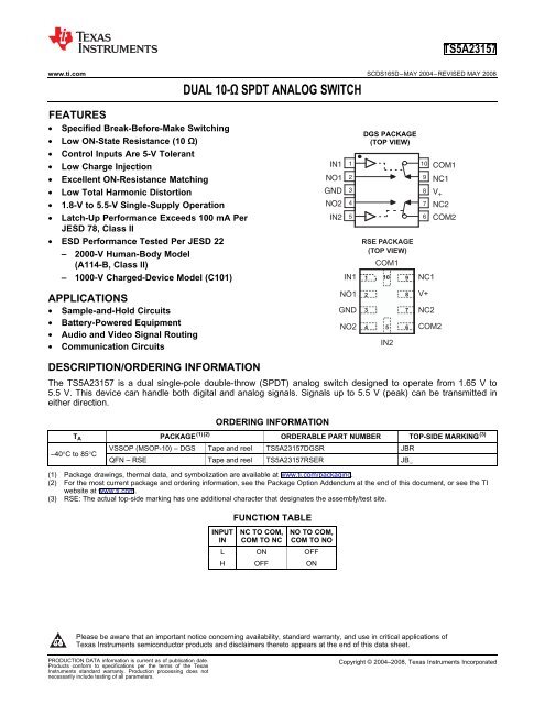
TS5A23157SCDS165D–MAY 2004–REVISED MAY 2008 ................................................................................................................................................................ www.ti.comPIN DESCRIPTIONPIN NO. NAME DESCRIPTION1 IN1 Digital control to connect COM to NO or NC2 NO1 Normally open3 GND Digital ground4 NO2 Normally open5 IN2 Digital control to connect COM to NO or NC6 COM2 Common7 NC2 Normally closed8 V + Power supply9 NC1 Normally closed<strong>10</strong> COM1 CommonPARAMETER DESCRIPTIONSYMBOLV COMV NCV NOr onΔr onr on(flat)I NC(OFF)I NO(OFF)I NC(ON)I NO(ON)I COM(ON)V IHV ILV INI IH , I ILt ONt OFFt BBMQ CC NC(OFF)C NO(OFF)C NC(ON)C NO(ON)C COM(ON)C INO ISOVoltage at COMVoltage at NCVoltage at NODESCRIPTIONResistance between COM and NC or COM and NO ports when the channel is ONDifference of r on between channelsDifference between the maximum and minimum value of r on in a channel over the specified range of conditionsLeakage current measured at the NC port, with the corresponding channel (NC to COM) in the OFF state underworst-case input and output conditionsLeakage current measured at the NO port, with the corresponding channel (NO to COM) in the OFF state underworst-case input and output conditionsLeakage current measured at the NC port, with the corresponding channel (NC to COM) in the ON state and the output(COM) being openLeakage current measured at the NO port, with the corresponding channel (NO to COM) in the ON state and the output(COM) being openLeakage current measured at the COM port, with the corresponding channel (NO to COM or NC to COM) in the ON stateand the output (NC or NO) being openMinimum input voltage for logic high for the control input (IN)Minimum input voltage for logic low for the control input (IN)Voltage at INLeakage current measured at INTurn-on time for the switch. This parameter is measured under the specified range of conditions and by the propagationdelay between the digital control (IN) signal and analog outputs (COM/NC/NO) signal when the switch is turning ON.Turn-off time for the switch. This parameter is measured under the specified range of conditions and by the propagationdelay between the digital control (IN) signal and analog outputs (COM/NC/NO) signal when the switch is turning OFF.Break-before-make time. This parameter is measured under the specified range of conditions and by the propagationdelay between the output of two adjacent analog channels (NC and NO) when the control signal changes state.Charge injection is a measurement of unwanted signal coupling from the control (IN) input to the analog (NC, NO, orCOM) output. This is measured in coulombs ) and measured by the total charge induced due to switching of the controlinput. Charge injection, Q C = C L × ΔV O , C L is the load capacitance and ΔV O is the change in analog output voltage.Capacitance at the NC port when the corresponding channel (NC to COM) is OFFCapacitance at the NO port when the corresponding channel (NC to COM) is OFFCapacitance at the NC port when the corresponding channel (NC to COM) is ONCapacitance at the NO port when the corresponding channel (NC to COM) is ONCapacitance at the COM port when the corresponding channel (COM to NC or COM to NO) is ONCapacitance of INOFF isolation of the switch is a measurement of OFF-state switch impedance. This is measured in dB in a specificfrequency, with the corresponding channel (NC to COM or NO to COM) in the OFF state. OFF isolation, O ISO = 20 LOG(V NC /V COM ) dB, V COM is the input and V NC is the output.<strong>10</strong> Submit Documentation Feedback Copyright © 2004–2008, Texas Instruments IncorporatedProduct Folder Link(s): TS5A23157
TS5A23157www.ti.com ................................................................................................................................................................ SCDS165D–MAY 2004–REVISED MAY 2008SYMBOLX TALKBWI +ΔI +PARAMETER DESCRIPTION (continued)DESCRIPTIONCrosstalk is a measurement of unwanted signal coupling from an ON channel to an OFF channel (NC to NO or NO toNC). This is measured at a specific frequency and in dB. Crosstalk, X TALK = 20 log (V NC1 /V NO1 ), V NO1 is the input andV NC1 is the output.Bandwidth of the switch. This is the frequency where the gain of an ON channel is –3 dB below the dc gain. Gain ismeasured from the equation, 20 log (V NC /V COM ) dB, where V NC is the output and V COM is the input.Static power-supply current with the control (IN) pin at V + or GNDThis is the increase in I + for each control (IN) input that is at the specified voltage, rather than at V + or GND.Copyright © 2004–2008, Texas Instruments Incorporated Submit Documentation Feedback 11Product Folder Link(s): TS5A23157
TS5A23157SCDS165D–MAY 2004–REVISED MAY 2008 ................................................................................................................................................................ www.ti.comPARAMETER MEASUREMENT INFORMATIONV NONCNOCOMV COMV +I COMr on V COM V NONCChannel ONV ININI COMV IN = V IH or V ILV NCV +GNDFigure <strong>10</strong>. ON-State Resistance on )OFF-State Leakage CurrentChannel OFFV NCNCNOCOMV IN = V IH or V ILV V COM NC or V NO = 0 to V +orV COM = 0 to V +V ININON-State Leakage CurrentChannel ONV IN = V IH or V ILV NOV +GNDV NC or V NO = 0 to V + , V COM = OpenorV NC or V NO = Open, V COM = 0 to V +Figure 11. ON- and OFF-State Leakage Current (I COM(ON) , I NC(OFF) , I NO(OFF) , I NC(ON) , I NO(ON) )CapacitanceMeterV COMV NCV BIAS VIN INNO, COM, and IN inputs duringON and OFF conditions.V IN = V IH or V ILV NOCapacitance is measured at NC,GNDV BIAS = V + or GNDFigure 12. Capacitance IN , C COM(ON) , C NC(OFF) , C NO(OFF) , C NC(ON) , C NO(ON) )12 Submit Documentation Feedback Copyright © 2004–2008, Texas Instruments IncorporatedProduct Folder Link(s): TS5A23157
TS5A23157www.ti.com ................................................................................................................................................................ SCDS165D–MAY 2004–REVISED MAY 2008PARAMETER MEASUREMENT INFORMATION (continued)LogicInputV NC or V NONC or NOV +V ININNC or NO COMGNDTESTR LC LV NCV NOGND V +t ON 500 Ω 50 pFV + GNDV COMGND V +t OFF 500 Ω 50 pFV + GNDR L C LLogicV IN50%50%Inputt ONt OFF<strong>Switch</strong>90% 90%VOutput COMFigure 13. Turn-On (t ON ) and Turn-Off (t OFF ) TimeV +t r < 5 nst f < 5 nsV IV INNC or NONC or NOINCOMV COMLogicInputV INR L C LV COMt BBM<strong>Switch</strong>Output050%90% 90%LogicInputGNDV I = V + /2R L = 50 ΩC L = 35 pFFigure 14. Break-Before-Make (t BBM ) TimeNetwork AnalyzerV +SourceSignal50 V NC NCChannel ON: NC to COMCOM V COMGain20 log V COMdBV NC50 V INNOINNetwork Analyzer SetupGNDSource Power = 0 dBMDC Bias = 350 mVFigure 15. Frequency Response (BW)Copyright © 2004–2008, Texas Instruments Incorporated Submit Documentation Feedback 13Product Folder Link(s): TS5A23157
TS5A23157SCDS165D–MAY 2004–REVISED MAY 2008 ................................................................................................................................................................ www.ti.comPARAMETER MEASUREMENT INFORMATION (continued)Network AnalyzerV +SourceSignal50 V NC NCChannel OFF: NC to COMCOM 50 NOOFF Isolation20 log VCOMdBV NC50 GNDNetwork Analyzer SetupSource Power = 0 dBMDC Bias = 350 mVFigure 16. OFF Isolation (O ISO )Network Analyzer50 NCV +50 NOV NCV COMCrosstalk20 log V NOChannel ON: NC to COMChannel OFF: NO to COMSourceSignalV NOGND50 Network Analyzer SetupV NCdBSource Power = 0 dBMDC Bias = 350 mVFigure 17. Crosstalk (X TALK)V GEN+LogicInputV +R GENNC or NONC or NO COMV IN INGNDV INHLogicVInput INOFF ON OFFV INLV OUTV OUTR L C LV GEN = 0R GEN = 0R L = 1 MΩC L = 35 pFQ C = C L × ∆V OUT∆V OUTV IN = V IH or V ILFigure 18. Charge Injection (Q C )14 Submit Documentation Feedback Copyright © 2004–2008, Texas Instruments IncorporatedProduct Folder Link(s): TS5A23157
TS5A23157www.ti.com ................................................................................................................................................................ SCDS165D–MAY 2004–REVISED MAY 2008PARAMETER MEASUREMENT INFORMATION (continued)AnalyzerV O<strong>10</strong> FV + /2R LNCV +<strong>10</strong> FChannel ON: COM to NCV SOURCE = 0.5 V P-Pf SOURCE = 600 Hz to 20 kHzR L = 600 ΩC L = 50 pFC LNOCOMR LV SOURCEGNDFigure 19. Total Harmonic Distortion (THD)Copyright © 2004–2008, Texas Instruments Incorporated Submit Documentation Feedback 15Product Folder Link(s): TS5A23157
PACKAGE OPTION ADDENDUMwww.ti.com8-Dec-2009PACKAGING INFORMATIONOrderable Device Status (1) PackageTypePackageDrawingPins PackageQtyTS5A23157DGSR ACTIVE MSOP DGS <strong>10</strong> 2500 Green (RoHS &no Sb/Br)TS5A23157DGSRE4 ACTIVE MSOP DGS <strong>10</strong> 2500 Green (RoHS &no Sb/Br)TS5A23157DGSRG4 ACTIVE MSOP DGS <strong>10</strong> 2500 Green (RoHS &no Sb/Br)TS5A23157DGST ACTIVE MSOP DGS <strong>10</strong> 250 Green (RoHS &no Sb/Br)TS5A23157DGSTE4 ACTIVE MSOP DGS <strong>10</strong> 250 Green (RoHS &no Sb/Br)TS5A23157DGSTG4 ACTIVE MSOP DGS <strong>10</strong> 250 Green (RoHS &no Sb/Br)TS5A23157RSER ACTIVE UQFN RSE <strong>10</strong> 3000 Green (RoHS &no Sb/Br)TS5A23157RSERG4 ACTIVE UQFN RSE <strong>10</strong> 3000 Green (RoHS &no Sb/Br)Eco Plan (2) Lead/Ball Finish MSL Peak Temp (3)CU NIPDAUCU NIPDAUCU NIPDAUCU NIPDAUCU NIPDAUCU NIPDAUCU NIPDAUCU NIPDAULevel-1-260C-UNLIMLevel-1-260C-UNLIMLevel-1-260C-UNLIMLevel-1-260C-UNLIMLevel-1-260C-UNLIMLevel-1-260C-UNLIMLevel-1-260C-UNLIMLevel-1-260C-UNLIM(1) The marketing status values are defined as follows:ACTIVE: Product device recommended for new designs.LIFEBUY: TI has announced that the device will be discontinued, and a lifetime-buy period is in effect.NRND: Not recommended for new designs. Device is in production to support existing customers, but TI does not recommend using this part ina new design.PREVIEW: Device has been announced but is not in production. Samples may or may not be available.OBSOLETE: TI has discontinued the production of the device.(2) Eco Plan - The planned eco-friendly classification: Pb-Free (RoHS), Pb-Free (RoHS Exempt), or Green (RoHS & no Sb/Br) - please checkhttp://www.ti.com/productcontent for the latest availability information and additional product content details.TBD: The Pb-Free/Green conversion plan has not been defined.Pb-Free (RoHS): TI's terms "Lead-Free" or "Pb-Free" mean semiconductor products that are compatible with the current RoHS requirementsfor all 6 substances, including the requirement that lead not exceed 0.1% by weight in homogeneous materials. Where designed to be solderedat high temperatures, TI Pb-Free products are suitable for use in specified lead-free processes.Pb-Free (RoHS Exempt): This component has a RoHS exemption for either 1) lead-based flip-chip solder bumps used between the die andpackage, or 2) lead-based die adhesive used between the die and leadframe. The component is otherwise considered Pb-Free (RoHScompatible) as defined above.Green (RoHS & no Sb/Br): TI defines "Green" to mean Pb-Free (RoHS compatible), and free of Bromine (Br) and Antimony (Sb) based flameretardants (Br or Sb do not exceed 0.1% by weight in homogeneous material)(3)MSL, Peak Temp. -- The Moisture Sensitivity Level rating according to the JEDEC industry standard classifications, and peak soldertemperature.Important Information and Disclaimer:The information provided on this page represents TI's knowledge and belief as of the date that it isprovided. TI bases its knowledge and belief on information provided by third parties, and makes no representation or warranty as to theaccuracy of such information. Efforts are underway to better integrate information from third parties. TI has taken and continues to takereasonable steps to provide representative and accurate information but may not have conducted destructive testing or chemical analysis onincoming materials and chemicals. TI and TI suppliers consider certain information to be proprietary, and thus CAS numbers and other limitedinformation may not be available for release.In no event shall TI's liability arising out of such information exceed the total purchase price of the TI part(s) at issue in this document sold by TIto Customer on an annual basis.OTHER QUALIFIED VERSIONS OF TS5A23157 :•Automotive: TS5A23157-Q1NOTE: Qualified Version Definitions:Addendum-Page 1
PACKAGE OPTION ADDENDUMwww.ti.com8-Dec-2009•Automotive - Q<strong>10</strong>0 devices qualified for high-reliability automotive applications targeting zero defectsAddendum-Page 2
PACKAGE MATERIALS INFORMATIONwww.ti.com31-Jul-20<strong>10</strong>TAPE AND REEL INFORMATION*All dimensions are nominalDevicePackageTypePackageDrawingPins SPQ ReelDiameter(mm)ReelWidthW1 (mm)A0(mm)B0(mm)K0(mm)P1(mm)W(mm)Pin1QuadrantTS5A23157DGSR MSOP DGS <strong>10</strong> 2500 330.0 12.4 5.3 3.4 1.4 8.0 12.0 Q1TS5A23157RSER UQFN RSE <strong>10</strong> 3000 179.0 8.4 1.75 2.25 0.65 4.0 8.0 Q1Pack Materials-Page 1
PACKAGE MATERIALS INFORMATIONwww.ti.com31-Jul-20<strong>10</strong>*All dimensions are nominalDevice Package Type Package Drawing Pins SPQ Length (mm) Width (mm) Height (mm)TS5A23157DGSR MSOP DGS <strong>10</strong> 2500 358.0 335.0 35.0TS5A23157RSER UQFN RSE <strong>10</strong> 3000 203.0 203.0 35.0Pack Materials-Page 2
IMPORTANT NOTICETexas Instruments Incorporated and its subsidiaries (TI) reserve the right to make corrections, modifications, enhancements, improvements,and other changes to its products and services at any time and to discontinue any product or service without notice. Customers shouldobtain the latest relevant information before placing orders and should verify that such information is current and complete. All products aresold subject to TI’s terms and conditions of sale supplied at the time of order acknowledgment.TI warrants performance of its hardware products to the specifications applicable at the time of sale in accordance with TI’s standardwarranty. Testing and other quality control techniques are used to the extent TI deems necessary to support this warranty. Except wheremandated by government requirements, testing of all parameters of each product is not necessarily performed.TI assumes no liability for applications assistance or customer product design. Customers are responsible for their products andapplications using TI components. To minimize the risks associated with customer products and applications, customers should provideadequate design and operating safeguards.TI does not warrant or represent that any license, either express or implied, is granted under any TI patent right, copyright, mask work right,or other TI intellectual property right relating to any combination, machine, or process in which TI products or services are used. Informationpublished by TI regarding third-party products or services does not constitute a license from TI to use such products or services or awarranty or endorsement thereof. Use of such information may require a license from a third party under the patents or other intellectualproperty of the third party, or a license from TI under the patents or other intellectual property of TI.Reproduction of TI information in TI data books or data sheets is permissible only if reproduction is without alteration and is accompaniedby all associated warranties, conditions, limitations, and notices. Reproduction of this information with alteration is an unfair and deceptivebusiness practice. TI is not responsible or liable for such altered documentation. Information of third parties may be subject to additionalrestrictions.Resale of TI products or services with statements different from or beyond the parameters stated by TI for that product or service voids allexpress and any implied warranties for the associated TI product or service and is an unfair and deceptive business practice. TI is notresponsible or liable for any such statements.TI products are not authorized for use in safety-critical applications (such as life support) where a failure of the TI product would reasonablybe expected to cause severe personal injury or death, unless officers of the parties have executed an agreement specifically governingsuch use. Buyers represent that they have all necessary expertise in the safety and regulatory ramifications of their applications, andacknowledge and agree that they are solely responsible for all legal, regulatory and safety-related requirements concerning their productsand any use of TI products in such safety-critical applications, notwithstanding any applications-related information or support that may beprovided by TI. Further, Buyers must fully indemnify TI and its representatives against any damages arising out of the use of TI products insuch safety-critical applications.TI products are neither designed nor intended for use in military/aerospace applications or environments unless the TI products arespecifically designated by TI as military-grade or "enhanced plastic." Only products designated by TI as military-grade meet militaryspecifications. Buyers acknowledge and agree that any such use of TI products which TI has not designated as military-grade is solely atthe Buyer's risk, and that they are solely responsible for compliance with all legal and regulatory requirements in connection with such use.TI products are neither designed nor intended for use in automotive applications or environments unless the specific TI products aredesignated by TI as compliant with ISO/TS 16949 requirements. Buyers acknowledge and agree that, if they use any non-designatedproducts in automotive applications, TI will not be responsible for any failure to meet such requirements.Following are URLs where you can obtain information on other Texas Instruments products and application solutions:ProductsApplicationsAudio www.ti.com/audio Communications and Telecom www.ti.com/communicationsAmplifiers amplifier.ti.com Computers and Peripherals www.ti.com/computersData Converters dataconverter.ti.com Consumer Electronics www.ti.com/consumer-appsDLP® Products www.dlp.com Energy and Lighting www.ti.com/energyDSP dsp.ti.com Industrial www.ti.com/industrialClocks and Timers www.ti.com/clocks Medical www.ti.com/medicalInterface interface.ti.com Security www.ti.com/securityLogic logic.ti.com Space, Avionics and Defense www.ti.com/space-avionics-defensePower Mgmt power.ti.com Transportation and www.ti.com/automotiveAutomotiveMicrocontrollers microcontroller.ti.com Video and Imaging www.ti.com/videoRFID www.ti-rfid.com Wireless www.ti.com/wireless-appsRF/IF and ZigBee® Solutionswww.ti.com/lprfTI E2E Community Home Pagee2e.ti.comMailing Address: Texas Instruments, Post Office Box 655303, Dallas, Texas 75265Copyright © 2011, Texas Instruments Incorporated