4-Pin Phototransistor Optocouplers - DeSantiX.iT
4-Pin Phototransistor Optocouplers - DeSantiX.iT
4-Pin Phototransistor Optocouplers - DeSantiX.iT
- No tags were found...

You also want an ePaper? Increase the reach of your titles
YUMPU automatically turns print PDFs into web optimized ePapers that Google loves.
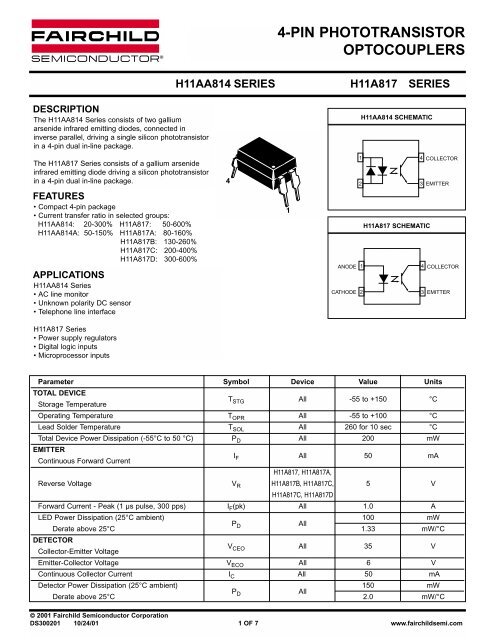
4-PIN PHOTOTRANSISTOROPTOCOUPLERSH11AA814 SERIES H11A817 SERIESDESCRIPTIONThe H11AA814 Series consists of two galliumarsenide infrared emitting diodes, connected ininverse parallel, driving a single silicon phototransistorin a 4-pin dual in-line package.H11AA814 SCHEMATICThe H11A817 Series consists of a gallium arsenideinfrared emitting diode driving a silicon phototransistorin a 4-pin dual in-line package.FEATURES• Compact 4-pin package• Current transfer ratio in selected groups:H11AA814: 20-300% H11A817: 50-600%H11AA814A: 50-150% H11A817A: 80-160%H11A817B: 130-260%H11A817C: 200-400%H11A817D: 300-600%APPLICATIONSH11AA814 Series• AC line monitor• Unknown polarity DC sensor• Telephone line interface4114 COLLECTOR23 EMITTERH11A817 SCHEMATICANODE 14 COLLECTORCATHODE 23 EMITTERH11A817 Series• Power supply regulators• Digital logic inputs• Microprocessor inputsParameter Symbol Device Value UnitsTOTAL DEVICEStorage TemperatureT STG All -55 to +150 °COperating Temperature T OPR All -55 to +100 °CLead Solder Temperature T SOL All 260 for 10 sec °CTotal Device Power Dissipation (-55°C to 50 °C) P D All 200 mWEMITTERContinuous Forward CurrentI F All 50 mAH11A817, H11A817A,Reverse Voltage V R H11A817B, H11A817C, 5 VH11A817C, H11A817DForward Current - Peak (1 µs pulse, 300 pps) I F (pk) All 1.0 ALED Power Dissipation (25°C ambient)100 mWP DAllDerate above 25°C 1.33 mW/°CDETECTORCollector-Emitter VoltageV CEO All 35 VEmitter-Collector Voltage V ECO All 6 VContinuous Collector Current I C All 50 mADetector Power Dissipation (25°C ambient)150 mWP DAllDerate above 25°C 2.0 mW/°C© 2001 Fairchild Semiconductor CorporationDS300201 10/24/01 1 OF 7 www.fairchildsemi.com
4-PIN PHOTOTRANSISTOROPTOCOUPLERSH11AA814 SERIES H11A817 SERIESELECTRICAL CHARACTERISTICS (T A = 25°C Unless otherwise specified.)INDIVIDUAL COMPONENT CHARACTERISTICSParameter Test Conditions Symbol Device Min Typ Max UnitEMITTERH11A817, H11A17A,(I F = 20 mA)H11A817B, H11A817C, 1.2 1.5V FH11A817DInput Forward VoltageV(I F = ±20 mA) H11AA814 1.2 1.5H11A817, H11A17A,Reverse Leakage Current (V R = 5.0 V) I R H11A817B, H11A817C, .001 10 µAH11A817DDETECTORCollector-Emitter Breakdown Voltage(I C = 1.0 mA, I F = 0) BV CEO ALL 35 100 VEmitter-Collector Breakdown Voltage (I E = 100 µA, I F = 0) BV ECO ALL 6 10 VCollector-Emitter Dark Current (V CE = 10V, I F = 0) I CEO ALL .025 100 nACollector-Emitter Capacitance (V CE = 0 V, f = 1 MHz) C CE ALL 8 pFTRANSFER CHARACTERISTICS (T A = 25°C Unless otherwise specified.)DC Characteristic Test Conditions Symbol Device Min Typ Max Unit(I F = ±1 mA, V CE = 5 V) (note 1) CTR H11AA814 20 300 %(I F = ±1 mA, V CE = 5 V) (note 1) CTR H11AA814A 50 150 %H11A817 50 600 %Current Transfer Ratio H11A817A 80 160 %(I F = 5 mA, V CE = 5 V) (note 1) CTR H11A817B 130 260 %H11A817C 200 400 %H11A817D 300 600 %Collector-EmitterSaturation Voltage(I C = 1 mA, I F = ±20 mA) V CE (SAT) ALL .1 .2 VAC CharacteristicRise Time (I C = 2 mA, V CE = 2 V, R L = 100#) (note 1) T R ALL 2.4 18 µsFall Time (I C = 2 mA, V CE = 2 V, R L = 100#) (note 1) T F ALL 2.4 18 µsISOLATION CHARACTERISTICSCharacteristic Test Conditions Symbol Min Typ Max UnitsInput-Output Isolation Voltage (note 3) (I I-O !"1 µA, 1 min.) V ISO 5300 Vac(rms)Isolation Resistance (V I-O = 500 VDC) R ISO 10 11 #Isolation Capacitance (V I-O = $, f = 1 MHz) C ISO 0.5 pfNOTES1. Current Transfer Ratio (CTR) = I C /I F x 100%.2. For test circuit setup and waveforms, refer to Figure 8.3. For this test, <strong>Pin</strong>s 1 and 2 are common, and <strong>Pin</strong>s 4, 5 and 6 are common.www.fairchildsemi.com 2 OF 7 10/24/01 DS300201
4-PIN PHOTOTRANSISTOROPTOCOUPLERSH11AA814 SERIES H11A817 SERIESFig. 1 Normalized CTR vs. Forward CurrentFig. 2 Normalized CTR vs. Ambient TemperatureNORMALIZED CTRCTR NORMALIZED @ IF = 5 mA, VCE = 5 V, TA = 25˚C1.41.20.80.60.40.21NORMALIZED CTRCTR NORMALIZED @ IF = 5 mA, VCE = 5 V, TA = 25˚C1.210.80.6I F = 5 mAI F = 10 mA005 10 15 20 25I F - FORWARD CURRENT (mA)300.4-50-25 0 +25 +50 +75T A - AMBIENT TEMPERATURE (˚C)+100VCE (SAT) - COLLECTOR-EMITTER SATURATION VOLTAGE (V).14.12.1.08.06.04.02Fig. 3 Collector-Emitter Saturation Voltagevs. Ambient TemperatureI F = 20 mAI C = 1 mA0-50 -25 025 50 75 100 125T A - AMBIENT TEMPERATURE (˚C)VF - FORWARD VOLTAGE (V)1.71.51.31.10.90.7Fig. 4 Forward Voltage vs. Forward CurrentT = 55˚CT = 25˚CT = 100˚C0.50.1 0.2 0.51.0 2.0 5 10 20 50 100I F - FORWARD CURRENT (mA)25Fig. 5 Collector Currentvs. Collector-Emitter VoltageI F = 20 mAIC - COLLECTOR CURRENT (mA)2015105I F = 10 mAI F = 5 mA00I F = 1 mA1 2 3 4 5 6 7 8 9 10V CE - COLLECTOR-EMITTER VOLTAGE (V)DS300201 10/24/01 3 OF 7 www.fairchildsemi.com
4-PIN PHOTOTRANSISTOROPTOCOUPLERSH11AA814 SERIES H11A817 SERIES10Fig. 6 Collector Leakage Currentvs. Ambient Temperature1000Fig. 7 Rise and Fall Timevs. Load ResistorICEO - COLLECTOR-EMITTER CURRENT (µA)110 -110 -210 -310 -410 -5V CE = 10 VTr/ Tf- RISE AND FALL TIME (µs)100101I F = 5 mAV CC = 5 VT A = 25˚Ct rtofft ont f10 -6025 50 75 100 1250.10.11 10 100T A - AMBIENT TEMPERATURE (˚C)R - LOAD RESISTOR (K#)Figure 8. Switching Time Test Circuit and WaveformsTEST CIRCUITWAVE FORMSV CC = 10VINPUT PULSEI F I C R L = 100#INPUTOUTPUT10%90%OUTPUT PULSEAdjust I F to produce IC = 2 mAt rt fwww.fairchildsemi.com 4 OF 7 10/24/01 DS300201
4-PIN PHOTOTRANSISTOROPTOCOUPLERSH11AA814 SERIES H11A817 SERIESPACKAGE DIMENSIONS (THROUGH HOLE)PACKAGE DIMENSIONS (SURFACE MOUNT)0.270 (6.86)0.250 (6.35)0.270 (6.86)0.250 (6.35)SEATING PLANE0.190 (4.83)0.175 (4.45)0.200 (5.08)0.115 (2.92)0.270 (6.86)0.250 (6.35)SEATING PLANE0.190 (4.83)0.175 (4.45)0.200 (5.08)0.115 (2.92)0.300 (7.62)TYP0.154 (3.90)0.120 (3.05)0.100 (2.54)TYP0.020 (0.51)MIN15°0.300 (7.62)typ0.016 (0.40)0.008 (0.20)0.070 (1.78)0.045 (1.14)0.100 (2.54)TYP0.020 (0.51)MIN0.022 (0.56)0.016 (0.41)0.315 (8.00)MIN0.405 (10.30)MAX0.016 (0.40)0.008 (0.20)Lead Coplanarity 0.004 (0.10) MAXPACKAGE DIMENSIONS (0.4” LEAD SPACING)FOOTPRINT DIMENSIONS (SURFACE MOUNT)0.270 (6.86)0.250 (6.35)0.070 (1.78)0.060 (1.52)SEATING PLANE0.190 (4.83)0.175 (4.45)0.200 (5.08)0.115 (2.92)0.270 (6.86)0.250 (6.35)0.415 (10.54)0.295 (7.49)0.100 (2.54)0.030 (0.76)0.154 (3.90)0.120 (3.05)0.004 (0.10)MIN0.016 (0.40)0.008 (0.20)0.100 (2.54)TYP0.400 (10.16)TYP0 to 15°NOTEAll dimensions are in inches (millimeters)DS300201 10/24/01 5 OF 7 www.fairchildsemi.com
4-PIN PHOTOTRANSISTOROPTOCOUPLERSH11AA814 SERIES H11A817 SERIESORDERING INFORMATIONOption Order Entry Identifier DescriptionS .S Surface Mount Lead BendSD .SD Surface Mount; Tape and reelW .W 0.4” Lead Spacing300 .300 VDE 0884300W .300W VDE 0884, 0.4” Lead Spacing3S .3S VDE 0884, Surface Mount3SD .3SD VDE 0884, Surface Mount, Tape & ReelCarrier Tape Specifications (“D” Taping Orientation)5.00 ± 0.200.30 ± 0.054.0 ± 0.112.0 ± 0.14.0 ± 0.1Ø1.55 ± 0.051.75 ± 0.1013.2 ± 0.27.5 ± 0.116.0 ± 0.34.95 ± 0.200.1 MAX 10.30 ± 0.20 Ø1.6 ± 0.1User Direction of FeedNOTEAll dimensions are millimeterswww.fairchildsemi.com 6 OF 7 10/24/01 DS300201
4-PIN PHOTOTRANSISTOROPTOCOUPLERSH11AA814 SERIES H11A817 SERIESDISCLAIMERFAIRCHILD SEMICONDUCTOR RESERVES THE THE RIGHT TO MAKE CHANGES WITHOUT FURTHER NOTICETO ANY PRODUCTS HEREIN TO IMPROVE RELIABILITY, FUNCTION OR DESIGN. FAIRCHILD DOES NOTASSUME ANY LIABILITY ARISING OUT OF THE APPLICATION OR USE OF ANY PRODUCT OR CIRCUITDESCRIBED HEREIN; NEITHER DOES IT CONVEY ANY LICENSE UNDER ITS PATENT RIGHTS, NOR THERIGHTS OF OTHERS.LIFE SUPPORT POLICYFAIRCHILD’S PRODUCTS ARE NOT AUTHORIZED FOR USE AS CRITICAL COMPONENTS IN LIFE SUPPORTDEVICES OR SYSTEMS WITHOUT THE EXPRESS WRITTEN APPROVAL OF THE PRESIDENT OF FAIRCHILDSEMICONDUCTOR CORPORATION. As used herein:1. Life support devices or systems are devices orsystems which, (a) are intended for surgicalimplant into the body,or (b) support or sustain life,and (c) whose failure to perform when properlyused in accordance with instructions for use providedin labeling, can be reasonably expected to result in asignificant injury of the user.2. A critical component in any component of a life supportdevice or system whose failure to perform can bereasonably expected to cause the failure of the lifesupport device or system, or to affect its safety oreffectiveness.DS300201 10/24/01 7 OF 7 www.fairchildsemi.com