LM1117/LM1117I 800mA Low-Dropout Linear Regulator
LM1117/LM1117I 800mA Low-Dropout Linear Regulator
LM1117/LM1117I 800mA Low-Dropout Linear Regulator

Create successful ePaper yourself
Turn your PDF publications into a flip-book with our unique Google optimized e-Paper software.
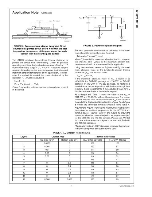
Application Note (Continued)<strong>LM1117</strong>/<strong>LM1117</strong>I1009193710091916FIGURE 5. Cross-sectional view of Integrated CircuitMounted on a printed circuit board. Note that the casetemperature is measured at the point where the leadscontact with the mounting pad surfaceThe <strong>LM1117</strong> regulators have internal thermal shutdown toprotect the device from over-heating. Under all possibleoperating conditions, the junction temperature of the <strong>LM1117</strong>must be within the range of 0˚C to 125˚C. A heatsink may berequired depending on the maximum power dissipation andmaximum ambient temperature of the application. To determineif a heatsink is needed, the power dissipated by theregulator, P D , must be calculated:I IN =I L +I GP D =(V IN -V OUT )I L +V IN I GFigure 6 shows the voltages and currents which are presentin the circuit.FIGURE 6. Power Dissipation DiagramThe next parameter which must be calculated is the maximumallowable temperature rise, T R (max):T R (max) = T J (max)-T A (max)where T J (max) is the maximum allowable junction temperature(125˚C), and T A (max) is the maximum ambient temperaturewhich will be encountered in the application.Using the calculated values for T R (max) and P D , the maximumallowable value for the junction-to-ambient thermalresistance (θ JA ) can be calculated:θ JA =T R (max)/P DIf the maximum allowable value for θ JA is found to be≥136˚C/W for SOT-223 package or ≥79˚C/W for TO-220package or ≥92˚C/W for TO-252 package, no heatsink isneeded since the package alone will dissipate enough heatto satisfy these requirements. If the calculated value for θ JAfalls below these limits, a heatsink is required.As a design aid, Table 1 shows the value of the θ JA ofSOT-223 and TO-252 for different heatsink area. The copperpatterns that we used to measure these θ JA s are shown atthe end of the Application Notes Section. Figure 7 and Figure8 reflects the same test results as what are in the Table 1Figure 9 and Figure 10 shows the maximum allowable powerdissipation vs. ambient temperature for the SOT-223 andTO-252 device. Figures Figure 11 and Figure 12 shows themaximum allowable power dissipation vs. copper area (in 2 )for the SOT-223 and TO-252 devices. Please see AN1028for power enhancement techniques to be used with SOT-223and TO-252 packages.*Application Note AN-1187 discusses improved thermal performanceand power dissipation for the LLP.TABLE 1. θ JA Different Heatsink AreaLayout Copper Area Thermal ResistanceTop Side (in 2 )* Bottom Side (in 2 ) (θ JA ,˚C/W) SOT-223 (θ JA ,˚C/W) TO-2521 0.0123 0 136 1032 0.066 0 123 873 0.3 0 84 604 0.53 0 75 545 0.76 0 69 526 1 0 66 477 0 0.2 115 848 0 0.4 98 709 0 0.6 89 6310 0 0.8 82 5711 0 1 79 5712 0.066 0.066 125 8911www.national.com