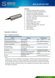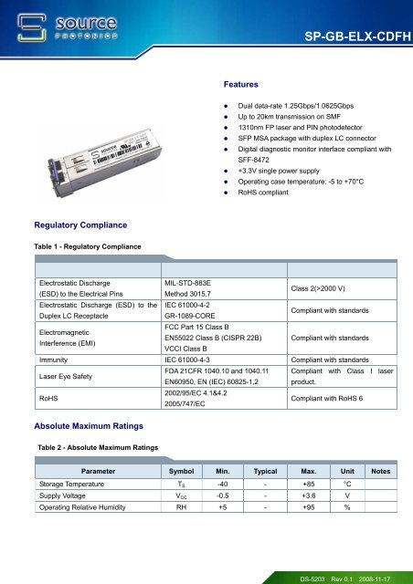
SP-GB-ELX-CDFH - Source Photonics
SP-GB-ELX-CDFH - Source Photonics
SP-GB-ELX-CDFH - Source Photonics

Create successful ePaper yourself
Turn your PDF publications into a flip-book with our unique Google optimized e-Paper software.
<strong>SP</strong>-<strong>GB</strong>-<strong>ELX</strong>-<strong>CDFH</strong>Recommended Operating ConditionsTable 3 – Recommended Operating ConditionsParameter Symbol Min. Typical Max. Unit NotesOperating Case Temperature T C -5 - +70 °CPower Supply Voltage V CC 3.13 3.3 3.47 VPower Supply Current I CC - - 300 mAPower Dissipation P D - - 1 WData Rate 1.0625 1.25 GbpsOptical CharacteristicsTable 4 – Optical CharacteristicsTransmitterParameter Symbol Min. Typical Max. Unit NotesCentre Wavelength λ C 1270 1310 1355 nmAverage Output Power P 0UT -8 -3 dBm 1P 0ut @TX Disable Asserted P 0UT -45 dBm 1Spectral Width (RMS) Δλ 2 4 nmExtinction Ratio EX 9 dBRise/Fall Time (20%~80%) t r /t f 0.26 ns 2Total JitterDeterministicJitter1.25GT J0.4311.0625G 0.431.25GD J1.0625G 0.210.2UI 3UI 3Optical Eye Mask IEEE 802.3ah and ANSI Fibre Channel compliant 4ReceiverCentre Wavelength λ C 1260 1570 nmReceiver Sensitivity P IN -22 dBm 5Receiver Overload P IN -3 dBm 5Return Loss 12 dBLOS Assert LOS A -35 dBmLOS Deassert LOS D -23 dBmLOS Hysteresis 1 4 dBTotal JitterDeterministicJitter1.25GT J0.7491.0625G 0.611.25GD J0.4621.0625G 0.36UI 3UI 3DS-5203 Rev 0.1 2008-11-17
<strong>SP</strong>-<strong>GB</strong>-<strong>ELX</strong>-<strong>CDFH</strong>Notes:1. The optical power is launched into SMF.2. Unfiltered, measured with a PRBS 2 7 -1 test pattern @1.25Gbps3. Meet the specified maximum output jitter requirements if the specified maximum input jitter is present.4. Measured with a PRBS 2 7 -1 test pattern @1.25Gbps/1.0625Gbps.5. Measured with a PRBS 2 7 -1 test pattern @1.25Gbps, worst-case extinction ratio, BER ≤1×10 -12 .Electrical CharacteristicsTable 5 – Electrical CharacteristicsTransmitterParameter Symbol Min. Typical Max. Unit NotesData Input Swing Differential V IN 500 2400 mV 1Input Differential Impedance Z IN 90 100 110 ΩTx_DIS Disable V D 2.0 V CC VTx_DIS Enable V EN GND GND+0.8 VTX_ Fault (Fault) 2.0 Vcc+0.3 VTX_ Fault (Normal) 0 0.8 VReceiverData Output Swing Differential V OUT 370 2000 mV 1Rx_LOS Fault V LOS-Fault 2.0 Vcc+0.3 VRx_LOS Normal V LOS-Normal GND GND+0.8 VNotes:1. Internally AC coupledRecommended Host Board Power Supply CircuitFigure 1, Recommended Host Board Power Supply CircuitDS-5203 Rev 0.1 2008-11-17
<strong>SP</strong>-<strong>GB</strong>-<strong>ELX</strong>-<strong>CDFH</strong>Recommended Interface CircuitHost BoardVcc (+3.3V)2×4.7K to 10KTX DisableSFP ModuleVccT10KTX FaultSerDat Out +Z=50TD +ProtocolICSERDESICSerDat Out -SerDat In +Z=50Z=50TD -RD +LaserdriverSerDat In -Z=50RD -AmplifierLOSVcc (+3.3V)3×4.7K to 10KMOD-DEF2MOD-DEF1MOD-DEF0EEPROMRGNDFigure 2, Recommended Interface CircuitPin DefinitionsFigure 3 below shows the pin numbering of SFP electrical interface. The pin functions are described in Table6 with some accompanying notes.TOP VIEWOF BOARDPin 20Pin 11Pin 10BOTTOM VIEWOF BOARDPin 1Figure 3, Pin ViewDS-5203 Rev 0.1 2008-11-17
<strong>SP</strong>-<strong>GB</strong>-<strong>ELX</strong>-<strong>CDFH</strong>Table 6 - Pin Function DefinitionsPin No. Name Function Plug Seq. Notes1 VeeT Transmitter Ground 12 TX Fault Transmitter Fault Indication 3 Note 13 TX Disable Transmitter Disable 3 Note 24 MOD-DEF2 Module Definition 2 3 Note 35 MOD-DEF1 Module Definition 1 3 Note 36 MOD-DEF0 Module Definition 0 3 Note 37 Rate Select Not Connected 38 LOS Loss of Signal 3 Note 49 VeeR Receiver Ground 110 VeeR Receiver Ground 111 VeeR Receiver Ground 112 RD- Inv. Received Data Out 3 Note 513 RD+ Received Data Out 3 Note 514 VeeR Receiver Ground 115 VccR Receiver Power 216 VccT Transmitter Power 217 VeeT Transmitter Ground 118 TD+ Transmit Data In 3 Note 619 TD- Inv. Transmit Data In 3 Note 620 VeeT Transmitter Ground 1Notes:1. TX Fault is an open collector output, which should be pulled up with a 4.7k~10kΩ resistor on the host board toa voltage between 2.0V and Vcc+0.3V. Logic 0 indicates normal operation; logic 1 indicates a laser fault ofsome kind. In the low state, the output will be pulled to less than 0.8V.2. TX Disable is an input that is used to shut down the transmitter optical output. It is pulled up within the modulewith a 4.7k~10kΩ resistor. Its states are:Low (0~0.8V):Transmitter on(>0.8V,
<strong>SP</strong>-<strong>GB</strong>-<strong>ELX</strong>-<strong>CDFH</strong>6. These are the differential transmitter inputs. They are AC-coupled, differential lines with 100Ω differentialtermination inside the module.EEPROM InformationThe SFP MSA defines a 256-byte memory map in EEPROM describing the transceiver’s capabilities, standardinterfaces, manufacturer, and other information, which is accessible over a 2 wire serial interface at the 8-bitaddress 1010000X (A0h). The memory contents refer to Table 7.Table 7 - EEPROM Serial ID Memory Contents (A0h)Addr.FieldSize(Bytes)Name of Field Hex Description0 1 Identifier 03 SFP1 1 Ext. Identifier 04 MOD42 1 Connector 07 LC3—10 8 Transceiver 00 00 00 02 12 00 01 01 Transmitter Code11 1 Encoding 01 8B10B12 1 BR, nominal 0D 1.25Gbps13 1 Reserved 0014 1Length(9um)-km1420km15 1 Length (9um) C8 20km16 1 Length (50um) 0017 1 Length (62.5um) 0018 1 Length (copper) 0019 1 Reserved 0020—35 16 Vendor name36 1 Reserved 0037—39 3 Vendor OUI 00 00 0040—55 16 Vendor PN53 4F 55 52 43 45 50 484F 54 4F 4E 49 43 53 2053 50 47 42 45 4C 58 4344 46 48 20 20 20 20 20“SOURCEPHOTONICS”(ASCⅡ)“<strong>SP</strong><strong>GB</strong><strong>ELX</strong><strong>CDFH</strong>” (ASCⅡ)56—59 4 Vendor rev xx xx xx xx ASC Ⅱ( “31 30 20 20” means 1.0 revision)60-61 2 Wavelength 05 1E 1310nm62 1 Reserved 0063 1 CC BASE xx Check sum of bytes 0 - 6264—65 2 Options 00 1A LOS, TX_FAULT and TX_DISABLE66 1 BR, max 0067 1 BR, min 0068—83 16 Vendor SNxx xx xx xx xx xx xx xxxx xx xx xx xx xx xx xxASC Ⅱ .DS-5203 Rev 0.1 2008-11-17
<strong>SP</strong>-<strong>GB</strong>-<strong>ELX</strong>-<strong>CDFH</strong>84—91 8Vendor datecode xx xx xx xx xx xx 20 20Year (2 bytes), Month (2 bytes), Day (2bytes)92 1 Diagnostic type 68 Diagnostics(Int.Cal)Diagnostics(Optional Alarm/warning flags,EnhancedSoft TX_FAULT and Soft TX_LOSoption93 1B0monitoring)94 1 SFF-8472 02 Diagnostics(SFF-8472 Rev 9.4)95 1 CC_EXT xx Check sum of bytes 64 - 9496—255 160 Vendor specificNote: The “xx” byte should be filled in according to practical case. For more information, please refer to therelated document of SFF-8472 Rev 9.5.Monitoring SpecificationThe digital diagnostic monitoring interface also defines another 256-byte memory map in EEPROM, whichmakes use of the 8 bit address 1010001X (A2h). Please see Figure 4. For detail EEPROM information,please refer to the related document of SFF-8472 Rev 9.5. The monitoring specification of this product isdescribed in Table 8.Figure 4, EEPROM Memory Map Specific Data Field DescriptionsTable 8- Monitoring SpecificationParameter Range Accuracy CalibrationTemperature -10 to 80°C ±3°C InternalVoltage 3.0 to 3.6V ±3% InternalBias Current 0 to 100mA ±10% InternalTX Power -8 to -2 dBm ±3dB InternalRX Power -23 to -2 dBm ±3dB InternalMechanical DiagramDS-5203 Rev 0.1 2008-11-17
<strong>SP</strong>-<strong>GB</strong>-<strong>ELX</strong>-<strong>CDFH</strong>Figure 5, Mechanical Design Diagram of the SFP with Spring-LatchOrder InformationTable 9 – Order InformationPart No. Application Data Rate Laser <strong>Source</strong> Fiber Type<strong>SP</strong>-<strong>GB</strong>-<strong>ELX</strong>-<strong>CDFH</strong> GbE 20Km 1.25Gbps 1310nm FP SMFWarningsHandling Precautions: This device is susceptible to damage as a result of electrostatic discharge (ESD). A staticfree environment is highly recommended. Follow guidelines according to proper ESD procedures.Laser Safety: Radiation emitted by laser devices can be dangerous to human eyes. Avoid eye exposure to director indirect radiation.Legal NoticeIMPORTANT NOTICE!All information contained in this document is subject to change without notice, at <strong>Source</strong> <strong>Photonics</strong>’s sole andabsolute discretion. <strong>Source</strong> <strong>Photonics</strong> warrants performance of its products to current specifications only inaccordance with the company’s standard one-year warranty; however, specifications designated as “preliminary”are given to describe components only, and <strong>Source</strong> <strong>Photonics</strong> expressly disclaims any and all warranties for saidproducts, including express, implied, and statutory warranties, warranties of merchantability, fi tness for a particularpurpose, and non-infringement of proprietary rights. Please refer to the company’s Terms and Conditions of Salefor further warranty information.DS-5203 Rev 0.1 2008-11-17
<strong>SP</strong>-<strong>GB</strong>-<strong>ELX</strong>-<strong>CDFH</strong><strong>Source</strong> <strong>Photonics</strong> assumes no liability for applications assistance, customer product design, software performance,or infringement of patents, services, or intellectual property described herein. No license, either express or implied,is granted under any patent right, copyright, or intellectual property right, and <strong>Source</strong> <strong>Photonics</strong> makes norepresentations or warranties that the product(s) described herein are free from patent, copyright, or intellectualproperty rights. Products described in this document are NOT intended for use in implantation or other life supportapplications where malfunction may result in injury or death to persons. <strong>Source</strong> <strong>Photonics</strong> customers using orselling products for use in such applications do so at their own risk and agree to fully defend and indemnify <strong>Source</strong><strong>Photonics</strong> for any damages resulting from such use or sale.THE INFORMATION CONTAINED IN THIS DOCUMENT IS PROVIDED ON AN “AS IS” BASIS. Customer agreesthat <strong>Source</strong> <strong>Photonics</strong> is not liable for any actual, consequential, exemplary, or other damages arising directly orindirectly from any use of the information contained in this document. Customer must contact <strong>Source</strong> <strong>Photonics</strong> toobtain the latest version of this publication to verify, before placing any order, that the information contained hereinis current.ContactU.S.A. Headquarters20550 Nordhoff StreetChatsworth, CA 91311USATel: +1-818-773-9044Fax: +1-818-773-0261ChinaBuilding #2&5, West Export Processing ZoneNo. 8 Kexin Road, Hi-Tech ZoneChengdu, 611731, ChinaTel: +86-28-8795-8788Fax: +86-28-8795-8789Taiwan9F, No 81, Shui Lee Rd.Hsinchu, Taiwan, R.O.C.Tel: +886-3-5169222Fax: +886-3-5169213© Copyright <strong>Source</strong> <strong>Photonics</strong>, Inc. 2007~2008All rights reservedDS-5203 Rev 0.1 2008-11-17