
Create successful ePaper yourself
Turn your PDF publications into a flip-book with our unique Google optimized e-Paper software.
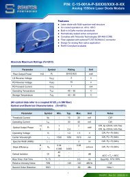
SFA-34-24T-HP-TDFIFeatures• Single Fiber, Integrated Diplexer Transceiver• 2x10 SFF pinout supports I 2 C digital diagnostics• Voice/Data FTTx ONT/ONU Applications• Compliant to FSAN G.984.5 Specifications• 1244 Mbps Tx, 2488 Mbps Rx Asymmetric Data Rate• 1310 nm Tx, 1490 nm Rx• Burst Mode Transmission• DDM TX Power• TX Burst Mode Detection, TX_SD• 28 dB link budget; 20 km reach• Compliant to IEC-60825 Class 1 laser diode• SC/APC fiber connector• RoHS compliant• Internal CalibrationRegulatory ComplianceTable 1 – Regulatory ComplianceFeature Standard PerformanceElectrostatic DischargeMIL-STD-883EClass 1(>500V for XFI(ESD) to the Electrical PinsMethod 3015.7pins, >2000V for other pins.)Electrostatic Discharge (ESD) to the IEC 61000-4-2Duplex LC ReceptacleGR-1089-CORECompatible with standardsFCC Part 15 Class BElectromagneticEN55022 Class B (CISPR 22B)Interference (EMI)VCCI Class BCompatible with standardsImmunity IEC 61000-4-3 Compatible with standardsLaser Eye SafetyFDA 21CFR 1040.10 and 1040.11 Compatible with Class I laserEN60950, EN (IEC) 60825-1,2 product.RoHS2002/95/EC 4.1&4.22005/747/ECCompliant with standards noteNote:In light of item 5 in Annex of 2002/95/EC, “Pb in the glass of cathode ray tubes, electronic components andfluorescent tubes.” and item 13 in Annex of 2005/747/EC, “Lead and cadmium in optical and filter glass.”,the two exemptions are being concerned for <strong>Source</strong> <strong>Photonics</strong> transceivers, because <strong>Source</strong> <strong>Photonics</strong>transceivers use glass, which may contain Pb, for components such as lenses, windows, isolators, andother electronic components.DS-6470 Rev 01 2011-03-28
SFA-34-24T-HP-TDFIAbsolute Maximum RatingsTable 2 – Absolute Maximum RatingsParameter Symbol Min. Typical Max. Unit NotesStorage Temperature T S -40 - +85 °CSupply VoltageV CC_ Rx -0.4 - +4.2 VV CC_ Tx -0.4 - V CC_ Rx+1 VOperating Relative Humidity RH 5 - 95 %Recommended Operating ConditionsTable 3 – Recommended Operating ConditionsParameterSymb Min. Typical Max. UnitolOperating Case Temperature T C -40 - 85 °COperating Voltage V CC 3.14 3.30 3.46 VTotal TX and RX Supply Current I CC - - 400 mAPower Dissipation P D - - 1.5 WBit Rate(Tx) BR - 1244.16 - MbpsBit Rate(Rx) BR - 2488.32 - MbpsTransmission Distance TD - - 20,000 mNotesOptical CharacteristicsTable 4 – Optical CharacteristicsTransmitterParameter Symbol Min. Typical Max. Unit NotesCenter Wavelength Range λ C 1290 - 1330 nmAverage Output Power P 0UT 0.5 - 5 dBmAverage Output Power (Laser Off) P 0UT-OFF - - -45 dBmSide Mode Suppression Ratio SMSR 30 - - dBSpectral Width (-20dB) λ 20 - - 1 nmExtinction Ratio ER 10 - - dB 1Optical Rise and Fall Time(20%-80%) T R /T F - 250 - psJitter Generation JG - - 0.2 UI 2Transmitter Output Eye Compliant with G.984.2 Figure 3ReceiverCenter Wavelength Range λ C 1480 - 1500 nmDS-6470 Rev 01 2011-03-28
SFA-34-24T-HP-TDFIReceived Optical Power P in -28 - -8 dBm 3Data Output Rise and Fall Time(20% to 80%)T R /T F - 160 - psSignal Detect Assertion Level SDA - - -31 dBmSignal Detect De-Assertion Level SDD -45 - - dBmHysteresis P SDA-SDD 0.5 - 6 dBRSSI Accuracy RSSI -3 - +3 dB1310nm Tx to 1490nm Rx Crosstalk - - -47 dB1555nm Rx to 1490nm Isolation 30 - - dBG.984.5 Wavelength Blocking FilterIsolation30 - - dBNotes:1. Measured with a PRBS 2 23 -1, NRZ, 50% duty cycle.2. 4kHz to 10MHz3. Measured with a PRBS 2 31 -1, 50% duty cycle.Electrical CharacteristicsTable 5 – Electrical CharacteristicsTransmitterParameter Symbol Min. Typical Max. Unit NotesDifferential Data Input Amplitude V IN,P-P 200 - 2400 mVpp 4Input Differential Impedance Z IN - 100 - Ω 5Tx Burst Enable Time T BURST_EN - - 12.86 ns 6Tx Burst Disable Time T BURST_DIS - - 12.86 ns 6Tx_BRST Voltage - Low V TX_ENB_Low 0 - 0.8 VTx_BRST Voltage – High V TX_ENB_Hith 2.0 - Vcc VTx_SD timing “D” T TX_SD-D - - 1000 nS 7Tx_SD timing “X” T TX_SD-X - - 350 nS 7Tx_SD Startup Time T TX_SD_Startup - - 3 S 7ReceiverDifferential Output Voltage 300 - 1200 mV 8Signal Detect Output HIGH Voltage V SD_High 2.4 - - V 9Signal Detect Output LOW Voltage V SD_Low - - 0.6 V 10Data Output Rise and Fall Time T R /T F - 160 - psNotes:4. TxD+/-. DC-coupled.5. TxD+/-.6. 16 bits data @1244Mbps7. Tx_SD:DS-6470 Rev 01 2011-03-28
SFA-34-24T-HP-TDFIFigure 1, Tx_SD Timing diagramFigure 2, Tx_SD Startup Timing diagram8. CML output, AC coupled(0.1µF)9. LVTTL with internal 10kΩ pull up resistor. Asserts HIGH when input data amplitude is above threshold.10. LVTTL. De-asserts LOW when input data amplitude is below threshold.DS-6470 Rev 01 2011-03-28
SFA-34-24T-HP-TDFIRecommended Interface CircuitV EET(12,16)+3.3V10μF0.1μF2X1μH0.1μFV CCT(11)V CCR(7)10μF0.1μFV EER(2,3,6)PON_TX_DISABLETX_BRST(13)+3.3VTXPTXNZ=50Z=50R1=NCR2=NCR1=NCTD+(14)TD-(15)R2=NC100Laser Driver(BM)GPON MACSerDesRXNRXPNCNC+3.3V+3.3V4.7-10KZ=50Z=50Tx_Fault(19)Tx_SD(20)RD-(9)RD+(10)LIA(CM)NCNC+3.3VSD(8)10KPON_SDAPON_SCL+3.3V2X4.7-10KSDA(18)SCL(17)MicroprocessorTemperatureSupply VoltageBias CurrentTx PowerRx PowerFigure 3, Recommended Interface CircuitDS-6470 Rev 01 2011-03-28
SFA-34-24T-HP-TDFIPin DefinitionsFigure 4, Pin ViewTable 6 – Pin definitionsPin Logic Symbol Name/Description Note1 NA NC No User Connection2 NA GND_Rx Digital Rx ground3 NA GND_Rx Digital Rx ground4 NA NC Reserved, No User Connection5 NA NC Reserved, No User Connection6 NA GND_Rx Digital Rx Ground7 NA Vcc_Rx Digital Rx Vcc8 LVTTL-O SDSignal Detect output, pull up internally (4.7kΩ). Assertshigh when input optical power level is above threshold9 CML-O RxD-RX data bar output, CML. 50Ω terminated to Vcc and ACcoupled to module output (0.1µF)10 CML-O RxD+RX data output, CML. 50Ω terminated to Vcc and AC coupledto module output (0.1µF)11 NA Vcc_Tx Digital Tx Vcc12 NA GND_Tx Digital Tx Ground13 LVTTL-I Tx_BRST Tx Burst Enable. LVTTL Input (1=TX on, 0=TX off)14 CML-I TxD+Tx data input, CML. Internally DC coupled. 100Ω differentialtermination.15 CML-I TxD-Tx data bar input, CML. Internally DC coupled. 100Ωdifferential termination.16 NA GND_Tx Digital Tx Ground17 LVTTL-I SCL I 2 C Clock input 118 LVTTL-I/O SDA I 2 C Data input/output 119 LVTTL-O Tx_Fault Module Transmitter Fault20 LVTTL-O Tx_SD Tx signal detectNote1. This pin is an open collector/drain output pin and shall be pulled up with 4.7K-10K ohms to a Host_Vcc onthe host board.DS-6470 Rev 01 2011-03-28
SFA-34-24T-HP-TDFI90 5A 2 V(Offset) Calibration 00 00 Offset for VCC calibration92 5C 3 Reserved 00 00 00 Reserved95 5F 1 Checksum xx Checksum96 60 2 Transceiver Temperature xx xx Temperature in C/25698 62 2 Supply Voltage xx xx Vcc100 64 2 TX Bias Current xx xx BIASMON102 66 2 TX Optical Output Power xx xx Back facet monitor104 68 2 RX Optical Input Power xx xx RSSI106 6A 2 Reserved 00 00 Reserved108 6C 2 Reserved 00 00 Reserved6E.7 1bit TX_DIS State x Soft TX disable state6E.6 1bit Soft TX Disable xWrite bit that allows software disablelaser output.6E.5 1bit Reserved. 0 Reserved1106E.4 1bit Rate Select State 0 NOT SUPPORTED.6E.3 1bit Rate Select 0 NOT SUPPORTED.6E.2 1bit TX_FAULT x Digital state of the TX Fault Output6E.1 1bit Rx LOS x Digital state of the Rx LOS Output6E.0 1bit Data Ready Bar xIndicates transceiver has achievedpower up and data is ready.6F.7 1bit Reserved 0 Reserved6F.6 1bit Reserved 0 Reserved6F.5 1bit Reserved 0 Reserved1116F.4 1bit Reserved 0 Reserved6F.3 1bit Reserved 0 Reserved6F.2 1bit Reserved x Reserved6F.1 1bit Reserved 0 Reserved6F.0 1bit Reserved x Reserved70.7 1bit Temperature too high alarm x Temperature too high alarm70.6 1bit Temperature too low alarm x Temperature too low alarm70.5 1bit VCC too high alarm x VCC too high alarm11270.4 1bit VCC too low alarm x VCC too low alarm70.3 1bit BIASMON too high alarm x BIASMON too high alarm70.2 1bit BIASMON too low alarm x BIASMON too low alarm70.1 1bit TX Power too high alarm x TX Power too high alarm70.0 1bit TX Power too low alarm x TX Power too low alarm71.7 1bit RX Power too high alarm x RX Power too high alarm71.6 1bit RX Power too low alarm x RX Power too low alarm11371.5 1bit Reserved interrupt status bit x Reserved interrupt status bit71.4 1bit Reserved interrupt status bit x Reserved interrupt status bit71.3 1bit Reserved interrupt status bit x Reserved interrupt status bit71.2 1bit Reserved interrupt status bit x Reserved interrupt status bitDS-6470 Rev 01 2011-03-28
SFA-34-24T-HP-TDFI71.1 1bit Reserved interrupt status bit x Reserved interrupt status bit71.0 1bit Reserved interrupt status bit x Reserved interrupt status bit114 72 1 Reserved 00 Reserved115 73 1 Reserved 00 Reserved74.7 1bit Temperature too high warning x Temperature too high warning74.6 1bit Temperature too low warning x Temperature too low warning74.5 1bit VCC too high warning x VCC too high warning11674.4 1bit VCC too low warning x VCC too low warning74.3 1bit BIASMON too high warning x BIASMON too high warning74.2 1bit BIASMON too low warning x BIASMON too low warning74.1 1bit TX Power too high warning x TX Power too high warning74.0 1bit TX Power too low warning x TX Power too low warning75.7 1bit RX Power too high warning x RX Power too high warning75.6 1bit RX Power too low warning x RX Power too low warning75.5 1bit Reserved interrupt status bit 0 Reserved interrupt status bit11775.4 1bit Reserved interrupt status bit 0 Reserved interrupt status bit75.3 1bit Reserved interrupt status bit 0 Reserved interrupt status bit75.2 1bit Reserved interrupt status bit 0 Reserved interrupt status bit75.1 1bit Reserved interrupt status bit 0 Reserved interrupt status bit75.0 1bit Reserved interrupt status bit 0 Reserved interrupt status bit118 76 1 Reserved 00 Reserved119 77 1 Reserved 00 Reserved120 78 8 Vendor Specific 00 00 00 00 00 00 00 00 Vendor SpecificTable 9 – Digital Diagnostic Specification (A2h)Data Address Parameter Range Accuracy96-97 Temperature -40 to 85°C ±3°C98-99 Vcc Voltage 0 to Vcc ±3%100-101 Bias Current 0 to 100mA ±10%102-103 TX Power -1 to 5dBm ±2dB104-105 RX Power -28 to -8dBm ±3dBOrder InformationTable 10 – Order InformationPart No. Application Data RateSFA-34-24T-HP-TDFI GPON ONTTX:1244.16Mb/sRX:2488.32Mb/sLaser<strong>Source</strong>1310nmDFBFiber TypeTempRangeSMF -40 to 85°CDS-6470 Rev 01 2011-03-28
SFA-34-24T-HP-TDFIWarningsHandling Precautions: This device is susceptible to damage as a result of electrostatic discharge (ESD).A static free environment is highly recommended. Follow guidelines according to proper ESD procedures.Laser Safety: Radiation emitted by laser devices can be dangerous to human eyes. Avoid eye exposure todirect or indirect radiation.Legal NoticeIMPORTANT NOTICE!All information contained in this document is subject to change without notice, at <strong>Source</strong> <strong>Photonics</strong>’s soleand absolute discretion. <strong>Source</strong> <strong>Photonics</strong> warrants performance of its products to current specificationsonly in accordance with the company’s standard one-year warranty; however, specifications designated as“preliminary” are given to describe components only, and <strong>Source</strong> <strong>Photonics</strong> expressly disclaims any and allwarranties for said products, including express, implied, and statutory warranties, warranties ofmerchantability, fitness for a particular purpose, and non-infringement of proprietary rights. Please refer tothe company’s Terms and Conditions of Sale for further warranty information.<strong>Source</strong> <strong>Photonics</strong> assumes no liability for applications assistance, customer product design, softwareperformance, or infringement of patents, services, or intellectual property described herein. No license,either express or implied, is granted under any patent right, copyright, or intellectual property right, and<strong>Source</strong> <strong>Photonics</strong> makes no representations or warranties that the product(s) described herein are freefrom patent, copyright, or intellectual property rights. Products described in this document are NOTintended for use in implantation or other life support applications where malfunction may result in injury ordeath to persons. <strong>Source</strong> <strong>Photonics</strong> customers using or selling products for use in such applications do soat their own risk and agree to fully defend and indemnify <strong>Source</strong> <strong>Photonics</strong> for any damages resulting fromsuch use or sale.THE INFORMATION CONTAINED IN THIS DOCUMENT IS PROVIDED ON AN “AS IS” BASIS. Customeragrees that <strong>Source</strong> <strong>Photonics</strong> is not liable for any actual, consequential, exemplary, or other damagesarising directly or indirectly from any use of the information contained in this document. Customer mustcontact <strong>Source</strong> <strong>Photonics</strong> to obtain the latest version of this publication to verify, before placing any order,that the information contained herein is current.ContactU.S.A. Headquarters China20550 Nordhoff Street Building #2&5, West Export Processing ZoneChatsworth, CA 91311 No. 8 Kexin Road, Hi-Tech ZoneUSAChengdu, 611731, ChinaTel: +1-818-773-9044 Tel: +86-28-8795-8788Fax: +1-818-773-0261 Fax: +86-28-8795-8789© Copyright <strong>Source</strong> <strong>Photonics</strong>, Inc. 2009~2011All rights reservedTaiwan9F, No 81, Shui Lee Rd.Hsinchu, Taiwan, R.O.C.Tel: +886-3-5169222Fax: +886-3-5169213DS-6470 Rev 01 2011-03-28