KT0803K - Elechouse
KT0803K - Elechouse
KT0803K - Elechouse
- No tags were found...

Create successful ePaper yourself
Turn your PDF publications into a flip-book with our unique Google optimized e-Paper software.
<strong>KT0803K</strong>• Operation ConditionTable 1: Operation ConditionParameter Symbol Operating Condition Min Typ Max Units1.8V Analog Supply 1 VDD Relative to GND 1.6 1.8 2.0 VIO/Regulator Supply IOVDD Relative to GND 1.6 3.6 VOperating Temp T A Ambient Temperature 0 25 70 °CNote: 1. No external voltage should be applied to this supply. Decoupling cap should be used instead• Specifications and FeaturesTable 2: FM Transmitter Functional Parameters (Unless otherwise noted TA = 0-70 o C,IOVDD=1.6~3.6 V, F in = 1 kHz)Parameter Symbol Test/OperatingConditionMin Nom Max UnitsFM Frequency Range F tx Pin 16 76 108 MHzCurrent Consumption I VDD Pin 4 with PA (poweramp.) at default powermode (PA_bias = 0,- 17 mARFGAIN[3:0]=1111)Standby Current I stand Pin 4 - 0.1 1 μASignal to Noise Ratio SNR V in = 0.7 V p-p , G in = 0 - 60 - dBTotal Harmonic Distortion THD V in = 0.7 V p-p , G in = 0 - 0.3 %Left/Right Channel Balance BAL V in = 0.7 V p-p , G in = 0 -0.2 - 0.2 dBStereo Separation (LeftRight) SEP V in = 0.7 V p-p , G in = 0 40 - dBSub Carrier Rejection Ratio SCR V in = 0.7 V p-p , G in = 0 - - 60 dBInput Swing 1 V in Single-ended input - 0.35 1.4 V RMSPGA Range for Audio Input G in -12 0 12 dBPGA Gain Step for Audio Input G step 1 4 dBRequired Input Common-Mode V cm Pin 5,7Voltage when DC-coupled0 0.8 1.8 VPower Supply Rejection 2 PSRR IOVDD = 1.9 ~ 3.6 V 40 - - dBGround Bounce Rejection 2 GSRR IOVDD = 1.9 ~ 3.6 V 40 - - dBInput Resistance (Audio Input) R in Pin 5, 7 120 150 180 kΩInput Capacitance (Audio Input) C in Pin 5, 7 0.5 0.8 1.2 pFAudio Input Frequency Band F in Pin 5, 7 20 - 15k HzTransmit Level V out 96 103 113 dBµVChannel Step STEP - 50 kHzPilot Deviation 7.5 15 kHzAudio Deviation 75 150 kHzFrequency ResponseMono,-3dB, ΔF=60kHz,50/75μs pre-emphasis30 15k HzPre-emphasis Time Constant T pre SIG_PROC = 1 - 50 - µsSIG_PROC = 0 - 75 - µsCrystal/External Clock CLK Input clock 32.768 KHz2-wire I 2 C Clock SCL Pin 14 0 100 400 kHzHigh Level Input Voltage V IH Pin 4, 8, 12, 14, 16 0.75 xIOVDD-IOVDD+ 0.25VLow Level Input Voltage V IL Pin 4, 8, 12, 14, 160.25 x- 0.25 -IOVDDVCopyright ©2009, KT Micro, Inc. 2
<strong>KT0803K</strong>Notes:1. Maximum is given on the condition of PGA gain = -12dB.2. Fin = 20 ~ 15k Hz.• Package and Pin ListTable 3: <strong>KT0803K</strong> Pin DefinitionPin Index Name I/O Type Function2 XI Analog I/O Crystal input.3 XO Analog I/O Crystal input4 IOVDD Power 1.6~3.3V external logic IOVDD1, 5,11,15 GND Ground Can be shorted together and connected to ground6 INL Analog Input Left channel audio input.7 INR Analog Input Right channel audio input.8 SW Digital Input Control bit. Chip enable, supply mode9, 12 GND Ground Ground10 RSTB Digital Input Reset (active low).13 SDA Digital I/O Serial data I/O.14 SCL Digital I/O Serial clock input.16 PA_OUT Analog Output FM RF output.GND116PA_OUTXI215GNDXOIOVDDGNDINLINRSW345678<strong>KT0803K</strong>14131211109SCLSDAGNDGNDRSTBGND•Figure 2: <strong>KT0803K</strong> Pin-outCopyright ©2009, KT Micro, Inc. 3
<strong>KT0803K</strong>accessed during the last read or write operation, incremented by one. This address stays valid betweenoperations as long as the chip power is maintained.Once the device address with the read/write select bit set to “1” is clocked in and acknowledged by the<strong>KT0803K</strong>, the current address data word is serially clocked out. The microcontroller does not respond withan input “0” but does generate a following stop condition (see Figure 4).CURRENT REGISTER READ PROCEDURES 0 1 1 1 1 1 0 R AA P7 bit address dataAcknowledge STOP conditionSTART condition READ command NO AcknowledgeFigure 4: Serial Interface ProtocolNote: The serial controller supports slave mode only. Any register can be addressed randomly.The address of the slave in the first 7 bits and the 8th bit tells whether the master is receiving data from theslave or transmitting data to the slave. The I 2 C write address is 0x7C and the read address is 0x7D.Slave Mode ProtocolWith reference to the clocking scheme shown in Figure 5, the serial interface operates in the followingmanner:Figure 5: Serial Interface Slave Mode ProtocolCLOCK and DATA TRANSITIONS: The SDA pin is normally pulled high with an external device. Dataon the SDA pin may change only during SCL low time periods (see Figure 6). Data changes during SCLhigh periods will indicate a start or stop condition as defined below.START CONDITION: A high-to-low transition of SDA with SCL high is a start condition which mustprecede any other command (see Figure 7).STOP CONDITION: A low-to-high transition of SDA with SCL high is a stop condition. After a readsequence, the stop command will place the <strong>KT0803K</strong> in a standby power mode (see Figure 7).ACKNOWLEDGE: All addresses and data words are serially transmitted to and from the <strong>KT0803K</strong> in 8-bit words. The <strong>KT0803K</strong> sends a “0” to acknowledge that it has received each word. This happens duringthe ninth clock cycle (see Figure 8).Copyright ©2009, KT Micro, Inc. 5
<strong>KT0803K</strong>Figure 6: Clock and Data TransitionsFigure 7: Start and Stop DefinitionFigure 8: AcknowledgeCopyright ©2009, KT Micro, Inc. 6
<strong>KT0803K</strong>Table 4: Transmission power settingRFGAINRFOUT0000 95.5 dBuV0001 96.5 dBuV0010 97.5 dBuV0011 98.2 dBuV0100 98.9 dBuV0101 100 dBuV0110 101.5 dBuV0111 102.8 dBuV1000 105.1 dBuV (107.2dBuV PA_BIAS=1)1001 105.6 dBuV (108dBuV, PA_BIAS=1)1010 106.2 dBuV (108.7dBuV, PA_BIAS=1)1011 106.5 dBuV (109.5dBuV, PA_BIAS=1)1100 107 dBuV (110.3dBuV, PA_BIAS=1)1101 107.4 dBuV (111dBuV, PA_BIAS=1)1110 107.7 dBuV (111.7dBuV, PA_BIAS=1)1111 (default setting) 108 dBuV (112.5dBuV, PA_BIAS=1)Register 0x02 (Address: 0x02, Default: 0x40)Bit 7 6 5 4 3 2 1 0<strong>KT0803K</strong> CHSEL[0] RFGAIN[3] - - MUTE PLTADJ - PHTCNSTKT0803 - - - - MUTE PLTADJ - PHTCNSTBits Type Default Label Description7 RW 0 CHSEL[0] LSB o CHSEL, additional to KT08036 RW 1 RFGAIN[3] MSB of RFGAIN5:4 RW 00 Reserved3 RW 0 MUTE Software Mute1: MUTE Enabled0: MUTE Disabled2 RW 0 PLTADJ Pilot Tone Amplitude Adjustment1: Amplitude high0: Amplitude low1 RW 0 NA Reserved0 RW 0 PHTCNST Pre-emphasis Time-Constant Set1: 50 μs (Europe, Australia)0: 75 μs (USA, Japan)Register 0x04 (Address: 0x04, Default: 0x04) - NewBit 7 6 5 4 3 2 1 0<strong>KT0803K</strong> - MONO PGA_LSB[1:0] FDEV[1:0] BASS[1:0]KT0803 - - - - -Bits Type Default Label Description7 RW 0 Reserved6 RW 0 MONO Force MONOCopyright ©2009, KT Micro, Inc. 8
<strong>KT0803K</strong>Bits Type Default Label Description6 RW 0 Reserved5 RW 0 PDPA Power Amplifier Power Down4 RW 0 Reserved3 RW 0 Reserved1 RW 0 Reserved0 RW 0 ReservedRegister 0x0E (Address: 0x0E, Default: 0x02) – NewBit 7 6 5 4 3 2 1 0<strong>KT0803K</strong> - - - - - - PA_BIAS -KT0803 - - - - - - - -Bits Type Default Label Description7:2 RW 0x00 Reserved1 RW 1 PA_BIAS PA bias current enhancement.0 RW 0 ReservedRegister 0x0F (Address: 0x0F, Read only) – NewBit 7 6 5 4 3 2 1 0<strong>KT0803K</strong> - - - PW_OK - SLNCID - -KT0803 - - - - - - - -Bits Type Default Label Description7 R NA Reserved6 R NA Reserved5 R NA Reserved4 R NA PW_OK Power OK indicator3 R NA Reserved2 R NA SLNCID 1 when Silence is detected1 R NA Reserved0 R NA ReservedRegister 0x10 (Address: 0x10, Default: 0x08) – NewBit 7 6 5 4 3 2 1 0<strong>KT0803K</strong> - - - LMTLVL[1:0] - - PGAMODKT0803 - - - - - - - -Bits Type Default Label Description7:5 RW 000 Reserved4:3 RW 01 LMTLVL[1:0] Internal audio limiter level control00 = 0.687501 = 0.7510 = 0.87511 = 0.96252:1 RW 00 Reserved0 RW 0 PGAMOD PGA mode selection0 = 4dB step (compatible with KT0803)1 = 1dB step with PGA_LSB[1:0 ] usedCopyright ©2009, KT Micro, Inc. 10
<strong>KT0803K</strong>Register 0x12 (Address: 0x12, Default: 0x80) - NewBit 7 6 5 4 3 2 1 0<strong>KT0803K</strong> SLNCDIS SLNCTHL[2:0] SLNCTHH[2:0] SW_MODKT0803 - - - - - - - -Bits Type Default Label Description7 RW 1 SLNCDIS Silence detection disable0 : enable1 : disable6:4 RW 000 SLNCTHL Silence detection low threshold000 : 0.25mv001 : 0.5mv010 : 1mv011 : 2mv100 : 4mv101 : 8mv110 : 16mv111 : 32mv3:1 RW 000 SLNCTHH Silence detection high threshold000 : 0.5mv001 : 1mv010 : 2mv011 : 4mv100 : 8mv101 : 16mv110 : 32mv111 : 64mv0 RW 0 SW_MOD Switching channel mode selection.0 = mute when changing channel1 = pa off when changing channelRegister 0x13 (Address: 0x13, Default: 0x80)Bit 7 6 5 4 3 2 1 0<strong>KT0803K</strong> RFGAIN[2] - - PA_CTRL - -KT0803 PA_HI_PW - - - - - - -Bits Type Default Label Description7 RW 1 RFGAIN[2] PA (Power amplifier) power (combined with Reg0x01[7:6] and Reg 0x02[6])to set up transmission range)6:3 RW 0000 Reserved2 RW 0 PA_CTRL Power amplifier structure selection0 = Internal power supply, KT0803 compatible1 = External power supply via external inductorNote : When an external inductor is used, this bitmust be set to 1 immediately after the Power OKindicator Reg 0x0F[4] is set to 1. Otherwise, thedevice may be destroyed!1:0 RW 00 ReservedCopyright ©2009, KT Micro, Inc. 11
<strong>KT0803K</strong>Register 0x14 (Address: 0x14, default 0x00) - NewBit 7 6 5 4 3 2 1 0<strong>KT0803K</strong> SLNCTIME SLNCCNTHIGH - -KT0803 - - - - - - - -Bits Type Default Label Description7:5 RW 000 SLNCTIME Silence detection low level and high level durationtime000 : 50ms001 : 100ms010 : 200ms011 : 400ms100 : 1s101 : 2s110 : 4s111 : 8s4:2 RW 000 SLNCCNTHIGH1:0 RW 00 ReservedSilence detection high level counter threshold000 : 15001 : 31010 : 63011 : 127100 : 255101 : 511110 : 1023111 : 2047Register 0x16 (Address 0x16, default: 0x00) - NewBit 7 6 5 4 3 2 1 0<strong>KT0803K</strong> - - - SLNCCNTLOW[2:0]KT0803 - - - - - - - -Bits Type Default Label Description7:3 RW 0x0 Reserved2:0 RW 000 SLNCCNTLOW[2:0] Silence low counter000 : 1001 : 2010 : 4011 : 8100 : 16101 : 32110 : 64111 : 128Copyright ©2009, KT Micro, Inc. 12
<strong>KT0803K</strong>Chip Enable and Mode ControlThere is one external pin SW (Pin 8) to enable the chip. The definition is shown below.Table 5: Pin SWMuteInputSWChip Mode IOVDD Clock Source0 Power off N/A N/A1 Power On 1.6~3.6V External crystal or clockThe FM transmitter can be muted by setting Register MUTE to “1” through I2C programming.Silence DetectionBit name Register location DescriptionSLNCDIS Reg 0x12[7] Setting to 0 to enable the silence detectionSLNCTIME[2:0] Reg 0x14[7:5] silence detection time windowSLNCTHL[2:0] Reg 0x12[6:4] Low threshold voltage of input signal for silence detectionSLNCTHH[2:0] Reg 0x12[3:1] High threshold voltage of input signal for silence detectionSLNCCNTTHL[2:0] Reg 0x14[4:2] # of time when the input signal amplitude is lower thanSLNCTHLSLNCCNTTHH[2:0] Reg 0x16[2:1] # of time when the input signal amplitude is higher thanSLNCTHHSLNCID Reg 0x0F[2] (Read only) Set to 1 when silence is detected.The silence detection scheme is enabled by setting SLNCDIS to 0.During the time defined by SLNTIME[2:0], the chip will be muted when the number of time when theinput amplitude is higher than the voltage defined by SLNCTHL[2:0] is lower than SLNCCNTTHL[2:0].The SLNCID bit is set to 0.When the input signal amplitude is higher than the voltage defined by SLNCTHH[2:0] and the number oftime when that happens is more than SLNCCNTTHH[2:0], the chip exits from the mute status and theSLNCID is cleared to 0.ResetThe global reset is issued after the RSTB pin set to “0” or automatic on-chip power-on reset. After a globalreset, all registers are reset to the default value.Copyright ©2009, KT Micro, Inc. 13
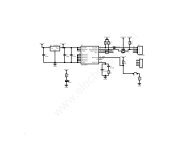
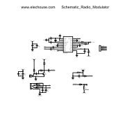
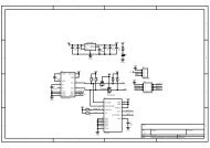
<strong>KT0803K</strong>• Typical Application CircuitsThe <strong>KT0803K</strong> can be integrated in a wide range of systems by requiring only a single power supply. Figure9 shows the external diagram for the drop-in replacement of KT0803.MCU(3.3 V CMOS Logic)OptionalI 2 C POR On/Off33nFSDASCLRSTBSWAntennaStereo AudioLine Input33nFINLINR<strong>KT0803K</strong>PA_OUTHFPin1,5,11,15 IOVDD GNDXIXOPin1,5,11,15<strong>KT0803K</strong>0Ω3.3V32.768 KHzXTALKT080333VFigure 9: Typical configuration for a drop-in replacementAs shown in the red block above, Pin 1, 5, 11 and 15 are VDD pins in KT0803 that arerequired to be connected to a decoupling capacitor. These four pins are GND pins in<strong>KT0803K</strong>. Customers can replace the decoupling capacitor of a 0-ohm resister withoutPCB board change.Copyright ©2009, KT Micro, Inc. 14
<strong>KT0803K</strong>MCU(3.3 V CMOS Logic)OptionalI 2 C POR On/OffStereo AudioLine Input33nFSDAINLINRSCL RSTB<strong>KT0803K</strong>SWPA_OUTAntenna33nFPin1,5,11,15 IOVDD GNDXIXO3.3V32.768 KHzFigure 10: Application that requires higher transmission power (>5dBm)Copyright ©2009, KT Micro, Inc. 15
<strong>KT0803K</strong>• Package OutlineSymbols(MILLIMETERS)(MILLIMETERS)MIN NOM MAX Symbols MIN NOM MAXA 1.75 D 9.70 9.90 10.10A1 0.10 0.25 E 5.80 6.00 6.20A2 1.30 1.40 1.50 E1 3.70 3.90 4.10A3 0.60 0.65 0.70 e 1.27BSCb 0.39 0.48 h 0.25 0.50b1 0.38 0.41 0.43 L 0.50 0.80c 0.21 0.26 L1 1.05BSCC1 0.19 0.20 0.21 θ 0 8°Copyright ©2009, KT Micro, Inc. 16
<strong>KT0803K</strong>• Revision HistoryV1.0 Official ReleaseV1.1 I2C addresses in textCopyright ©2009, KT Micro, Inc. 17
<strong>KT0803K</strong>• Contact InformationKT Micro Inc.22391 Gilberto, Suite DRancho Santa Margarita, CA 92688USATel: 949-713-4000Fax: 949-713-4004Email: sales@ktmicro.com北 京 昆 腾 微 电 子 有 限 公 司北 京 市 海 淀 区 蓝 靛 厂 东 路 2 号 金 源 时 代 商 务 中 心2 号 楼 B 座 8 层 (100089)电 话 :8610-88891945传 真 :8610-88891977电 子 邮 件 :sales@ktmicro.com网 站 :http://www.ktmicro.com.cnCopyright ©2009, KT Micro, Inc. 18